

BURR-BROWN REG1117, REG1117A User Manual
Please be aware that an important notice concerning availability, standard warranty, and use in critical applications of Texas Instruments
查询REG1117供应商
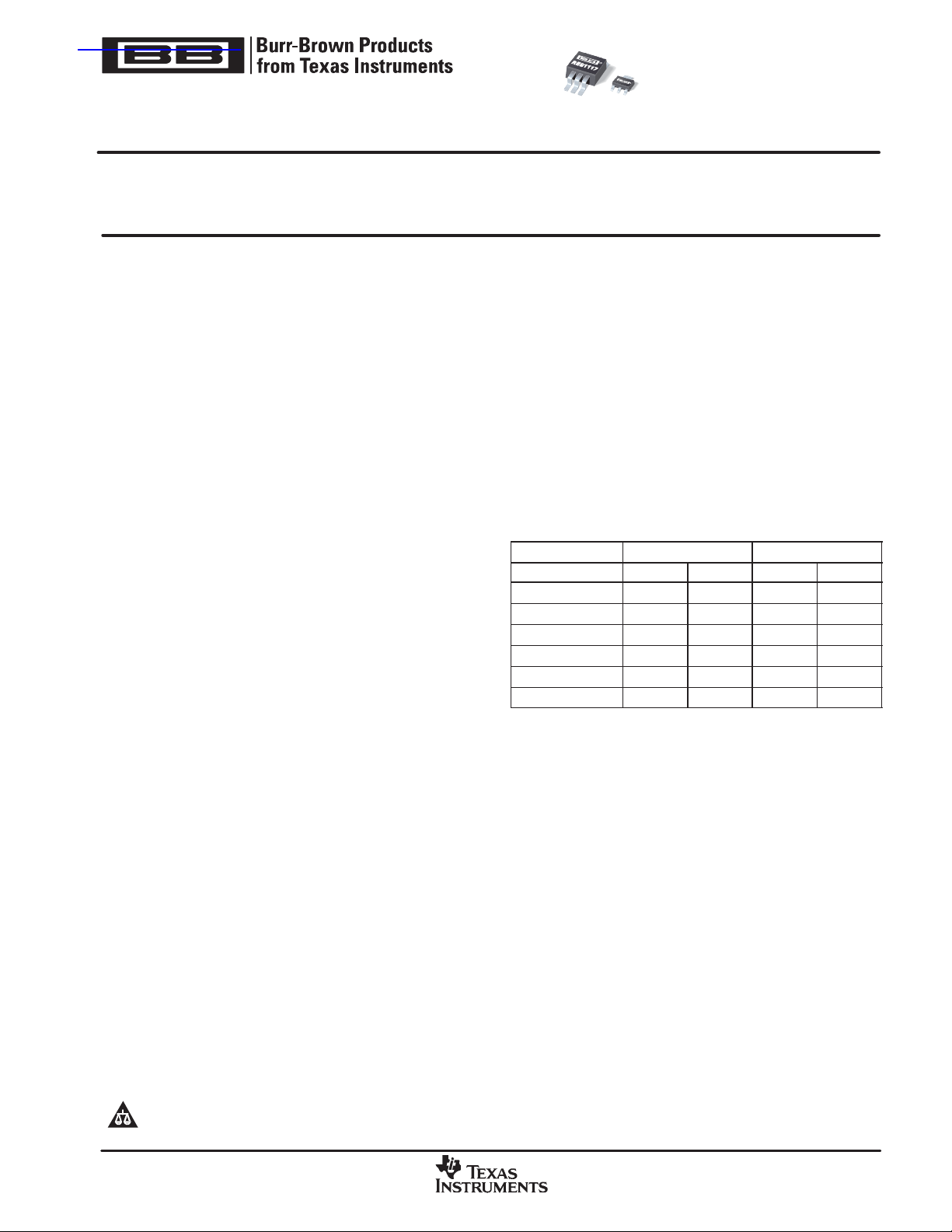
800mA and 1A Low Dropout Positive Regulator
1.8V, 2.5V, 2.85, 3.3V, 5V, and Adjustable
REG1117
REG1117A
SBVS001D − OCTOBER 1992 − REVISED JULY 2004
FEATURES
D FIXED AND ADJUSTABLE VERSIONS
D 2.85V MODEL FOR SCSI-2 ACTIVE
TERMINATION
D OUTPUT CURRENT:
REG1117: 800mA max
REG1117A: 1A max
D OUTPUT TOLERANCE: +1% max
D DROPOUT VOLTAGE:
REG1117: 1.2V max at IO = 800mA
REG1117A: 1.3V max at IO = 1A
D INTERNAL CURRENT LIMIT
D THERMAL OVERLOAD PROTECTION
D SOT-223 AND DDPAK SURFACE-MOUNT
PACKAGES
APPLICATIONS
D SCSI-2 ACTIVE TERMINATION
D HAND-HELD DATA COLLECTION DEVICES
D HIGH EFFICIENCY LINEAR REGULATORS
D BATTERY-POWERED INSTRUMENTATION
D BATTERY MANAGEMENT CIRCUITS FOR
NOTEBOOK AND PALMTOP PCs
D CORE VOLTAGE SUPPLY: FPGA, PLD, DSP,
CPU
DESCRIPTION
The REG1117 is a family of easy-to-use three-terminal
voltage regulators. The family includes a variety of fixedand adjustable-voltage versions, two currents (800mA and
1A) and two package types (SOT-223 and DDPAK). See
the chart below for available options.
Output voltage of the adjustable versions is set with two
external resistors. The REG1117 low dropout voltage
allows its use with as little as 1V input-output voltage
differential.
Laser trimming assures excellent output voltage accuracy
without adjustment. An NPN output stage allows output
stage drive to contribute to the load current for maximum
efficiency.
800mA 1A
VOLTAGE SOT-223 DDPAK SOT-223 DDPAK
1.8V n n
2.5V n n
2.85V n
3.3V n n
5V n n
Adjustable n n n
semiconductor products and disclaimers thereto appears at the end of this data sheet.
All trademarks are the property of their respective owners.
! !
www.ti.com
Copyright 1992−2004, Texas Instruments Incorporated
"#$$$%
"#$$$%
SBVS001D − OCTOBER 1992 − REVISED JULY 2004
www.ti.com
ABSOLUTE MAXIMUM RATINGS
(1)
Power Dissipation Internally Limited. . . . . . . . . . . . . . . . . . . . . . . . . .
Input Voltage +15V. . . . . . . . . . . . . . . . . . . . . . . . . . . . . . . . . . . . . . .
Operating Junction Temperature Range −40°C to +125°C. . . . . . . .
Storage Temperature Range −65°C to +150°C. . . . . . . . . . . . . . . . .
Lead Temperature (soldering, 10s)
(1)
Stresses above these ratings may cause permanent damage.
(2)
See Soldering Methods section.
(2)
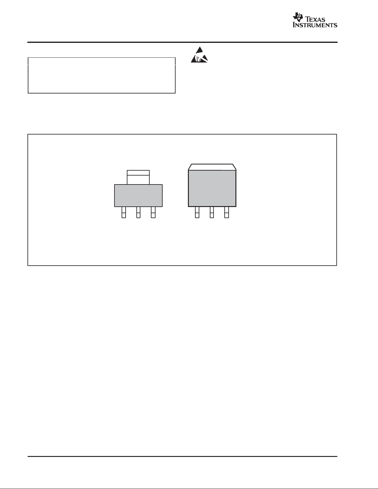
CONNECTION DIAGRAM
Front View
Plastic SOT−223
V
Ground
(Adj.)
OUT
(1)
+300°C. . . . . . . . . . . . . . . . .
Tab isV
V
IN
OUT
This integrated circuit can be damaged by ESD. Texas
Instruments recommends that all integrated circuits be
handled with appropriate precautions. Failure to observe
proper handling and installation procedures can cause damage.
ESD damage can range from subtle performance degradation to
complete device failure. Precision integrated circuits may be more
susceptible t o damage because very small parametric changes could
cause the device not to meet its published specifications.
Plastic DDPAK
Tab is
V
OUT
V
V
Ground
(Adj.)
(1)
OUT
IN
NOTE: (1) Adjustable−Voltage Model.
2
www.ti.com
−40°C to
−40 C to
−40°C to
−40 C to
−40°C to
−40 C to
−40°C to
−40 C to
−40°C to
−40 C to
"#$$$%
"#$$$%
SBVS001D − OCTOBER 1992 − REVISED JULY 2004
PACKAGE/ORDERING INFORMATION
PRODUCT VO/I
REG1117-2.85 2.85/800mA SOT223-3 DCY
REG1117-3.3 3.3/800mA SOT223-3 DCY
REG1117F-3.3 3.3/800mA DDPAK-3 KTT
REG1117-5 5V/800mA SOT223-3 DCY
REG1117 Adj./800mA SOT223-3 DCY
REG1117A-1.8 1.8V/1A SOT223-3 DCY
REG11 17F A-1.8 1.8/1A DDPAK-3 KTT
REG1117A-2.5 2.5/1A SOT223-3 DCY
REG11 17F A-2.5 2.5/1A DDPAK-3 KTT
REG1117FA-5 5/1A DDPAK-3 KTT
REG1117A Adj./1A SOT223-3 DCY
REG1117FA Adj./1A DDPAK-3 KTT
(1)
For the most current package and ordering information, see the Package Option Addendum located at the end of this data sheet.
O
PACKAGE-LEAD
(1)
PACKAGE
DESIGNATOR
OPERATING
TEMPERATURE
RANGE
−40°C to
+125°C
−40°C to
+125°C
+125°C
−40°C to
+125°C
−40°C to
+125°C
−40°C to
+125°C
+125°C
−40°C to
+125°C
+125°C
+125°C
−40°C to
+125°C
+125°C
PACKAGE
MARKING
BB11172
BB11174
BB1117F4
BB11175
BB1117
R111718
REG11 17F A1.8
R111725
REG1117FA2.5
BB1117FA5.0
BB1117A
REG1117FA
ORDERING
NUMBER
REG1117-2.85 Rails, 80
REG1117-2.85
REG1117-3.3 Rails, 80
REG1117-3.3
REG1117F-3.3KTTT
REG1117F-3.3/500
REG1117-5 Rails, 80
REG1117-5
REG1117 Rails, 80
REG1117
REG1117A-1.8 Rails, 80
REG1117A-1.8
REG1117FA-1.8KTTT
REG1117FA-1.8/500
REG1117A-2.5 Rails, 80
REG1117A-2.5
REG1117FA-2.5KTTT
REG1117FA-2.5/500
REG1117FA-5/KTTT
REG1117FA-5/500
REG1117A Rails, 80
REG1117A
REG1117FA/KTTT
REG1117FA/500
TRANSPORT
MEDIA,
QUANTITY
T ape and Reel,
2500
T ape and Reel,
2500
T ape and Reel,
50
T ape and Reel,
500
T ape and Reel,
2500
T ape and Reel,
2500
T ape and Reel,
2500
T ape and Reel,
50
T ape and Reel,
500
T ape and Reel,
2500
T ape and Reel,
50
T ape and Reel,
500
T ape and Reel,
50
T ape and Reel,
500
T ape and Reel,
2500
T ape and Reel,
50
T ape and Reel,
500
3
"#$$$%
"#$$$%
www.ti.com
SBVS001D − OCTOBER 1992 − REVISED JULY 2004
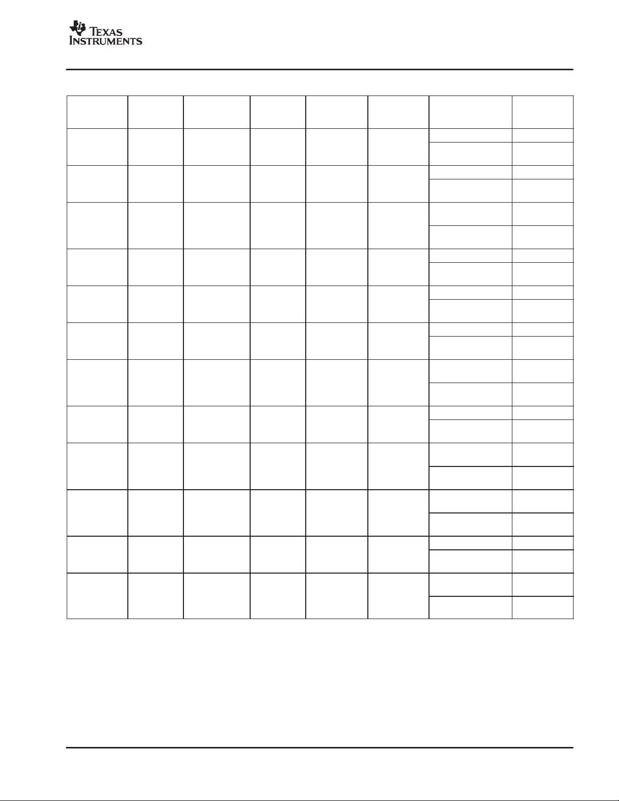
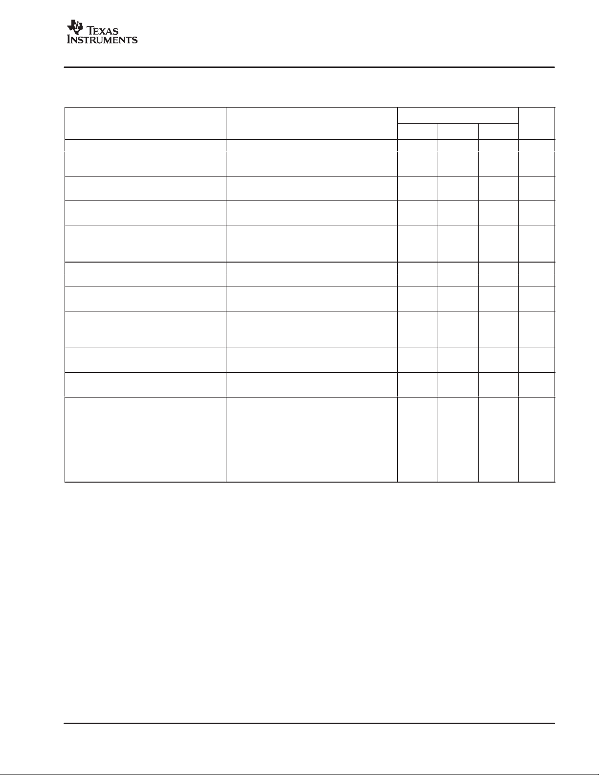
ELECTRICAL CHARACTERISTICS
At TJ = +25°C, unless otherwise noted.
REG1117, REG1 117A
PARAMETER CONDITION MIN TYP MAX UNIT
OUTPUT VOLTAGE
REG1117-2.85 IO = 10mA, VIN = 4.85V 2.820 2.85 2.880 V
See Note 1 IO = 0 to 800mA, VIN = 4.05V to 10V 2.790 2.85 2.910 V
REG1117-3.3 IO = 10mA, VIN = 5.3V 3.270 3.30 3.330 V
See Note 1 IO = 0 to 800mA, VIN = 4.8V to 10V 3.240 3.30 3.360 V
REG1117-5 IO = 10mA, VIN = 7V 4.950 5.00 5.050 V
See Note 1 IO = 0 to 800mA, VIN = 6.5V to 10V 4.900 5.00 5.100 V
REG1117A-1.8 IO = 10mA, VIN = 3.8V 1.782 1.8 1.818 V
See Note 1 IO = 0 to 1A, VIN = 3.8V to 10V 1.764 1.8 1.836 V
REG1117A-2.5 IO = 10mA, VIN = 4.5V 2.475 2.5 2.525 V
See Note 1 IO = 0 to 1A, VIN = 4.5V to 10V 2.450 2.5 2.550 V
REG1117A-5 IO = 10mA, VIN = 7V 4.950 5.0 5.050 V
See Note 1 IO = 0 to 1A, VIN = 7V to 10V 4.900 5.0 5.100 V
REFERENCE VOLTAGE
REG1117 (Adjustable) IO = 10mA, VIN − VO = 2V 1.238 1.250 1.262 V
See Note 1 IO = 10 to 800mA, VIN − VO = 1.4 to 10V 1.225 1.250 1.280 V
REG1117A (Adjustable) IO = 10mA, VIN − VO = 2V 1.238 1.250 1.262 V
See Note 1 IO = 10mA to 1A, VIN − VO = 1.4 to 10V 1.225 1.250 1.280 V
LINE REGULATION
(1)
(1)
(1)
(1)
(1)
(1)
(1)
(1)
(1)
(1)
(1)
(1)
(1)
(1)
(1)(2)
(1)(2)
(3)
IO = 0, VIN = 4.25 to 10V 1 7 mV
IO = 0, VIN = 4.8 to 10V 2 7 mV
IO = 0, VIN = 6.5 to 15V 3 10 mV
IO = 10mA, VIN − VO = 1.5 to 13.75V 0.1 0.4 %
IO = 10mA, VIN − VO = 1.5 to 13.75V 0.1 0.4 %
IO = 0, VIN = 3.8V to 10V 1 7 mV
IO = 0, VIN = 4.5V to 10V 1 7 mV
IO = 0, VIN = 7V to 15V 3 10 mV
IO = 0 to 800mA, VIN = 4.25V 2 10 mV
IO = 0 to 800mA, VIN = 4.8V 3 12 mV
IO = 0 to 800mA, VIN = 6.5V 3 15 mV
IO = 10 to 800mA, VIN − VO = 3V 0.1 0.4 %
IO = 10mA to 1A, VIN − VO = 3V 0.1 0.4 %
IO = 0 to 1A, VIN = 3.8V 2 10 mV
IO = 100mA 1.00 1.10 V
IO = 800mA 1.10 1.20 V
REG1117-2.85
REG1117-3.3
REG1117-5
REG1117 (Adjustable)
REG1117A (Adjustable)
REG1117A-1.8
REG1117A-2.5
REG1117A-5.0
LOAD REGULATION
REG1117-2.85
REG1117-3.3
REG1117-5
REG1117 (Adjustable)
REG1117A (Adjustable)
REG1117A-1.8
REG1117A-2.5 IO = 0 to 1A, VIN = 4.5V 2 10 mV
REG1117A-5 IO = 0 to 1A, VIN = 7.0V 3 15 mV
DROPOUT VOLTAGE
All Models
See Note 1 IO = 500mA 1.05 1.15 V
REG1117 Models
REG1117A IO = 1A 1.2 1.30 V
See Note 1 IO = 1A 1.2 1.55 V
(1)
Specification applies over the full specified junction temperature range, 0°C to +125°C.
(2)
REG1117 and REG1117A adjustable versions require a minimum load current for ±3% regulation.
(3)
Dropout voltage is the input voltage minus output voltage that produces a 1% decrease in output voltage.
(4)
Percentage change in unloaded output voltage before versus after a 30ms power pulse of IO = 800mA (REG11 17 models), IO = 1A (REG11 17A),
VIN − VO = 1.4V (reading taken 10ms after pulse).
4
"#$$$%
"#$$$%
www.ti.com
SBVS001D − OCTOBER 1992 − REVISED JULY 2004
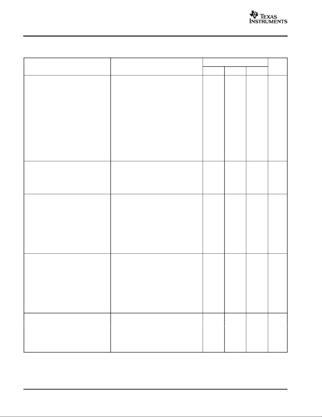
ELECTRICAL CHARACTERISTICS (continued)
At TJ = +25°C, unless otherwise noted.
REG1117, REG1 117A
PARAMETER UNITMAXTYPMINCONDITION
CURRENT LIMIT
REG1117 Models VIN − VO = 5V 800 950 1200 mA
REG1117A VIN − VO = 5V 1000 1250 1600 mA
MINIMUM LOAD CURRENT
(4)
(1)(2)
(1)
JC
JA
(1)
(1)(2)
(1)
VIN − VO = 13.75V 1.7 5 mA
VIN − VO = 5V 4 10 mA
IO = 10mA, VIN − VO = 1.4 to 10V 50 120 µA
IO = 10mA to 800mA, VIN − VO = 1.4 to 10V 0.5 5 µA
IO = 10mA to 1A, VIN − VO = 1.4 to 10V 0.5 5 µA
30ms Pulse 0.01 0.1 %/W
= 3V + 1VPP Ripple 62 dB
OUT
(Junction-to-Case at Tab)
dc 3 °C/W
(Junction-to-Case at Tab)
Adjustable Models
QUIESCENT CURRENT
Fixed-Voltage Models
ADJUSTABLE PIN CURRENT
vs Load Current, REG1117
vs Load Current, REG1117A
THERMAL REGULATION
All Models
RIPPLE REJECTION
All Models f = 120Hz, VIN − V
TEMPERATURE DRIFT
Fixed-Voltage Models TJ = 0°C to +125°C 0.5 %
Adjustable Models TJ = 0°C to +125°C 2 %
LONG-TERM STABILITY
All Models TA = 125°C, 1000Hr 0.3 %
OUTPUT NOISE
rms Noise, All Models f = 10Hz to 10kHz 0.003 %
THERMAL RESISTANCE
Thermal Resistance, q
3-Lead SOT-223 Surface-Mount 15 °C/W
3-Lead DDPAK Surface-Mount f > 50Hz 2 °C/W
Thermal Resistance, q
3-Lead DDPAK Surface-Mount No Heatsink 65 °C/W
(1)
Specification applies over the full specified junction temperature range, 0°C to +125°C.
(2)
REG1117 and REG1117A adjustable versions require a minimum load current for ±3% regulation.
(3)
Dropout voltage is the input voltage minus output voltage that produces a 1% decrease in output voltage.
(4)
Percentage change in unloaded output voltage before versus after a 30ms power pulse of IO = 800mA (REG11 17 models), IO = 1A (REG11 17A),
VIN − VO = 1.4V (reading taken 10ms after pulse).
5
 Loading...