

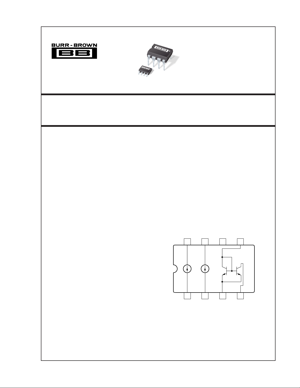
Burr Brown REF200AU, REF200AP Datasheet
®
REF200
REF200
REF200
DUAL CURRENT SOURCE/CURRENT SINK
FEATURES
● COMPLETELY FLOATING:
No Power Supply or Ground Connections
● HIGH ACCURACY: 100
µA ±0.5%
● LOW TEMPERATURE COEFFICIENT:
±25ppm/°C
● WIDE VOLTAGE COMPLIANCE:
2.5V to 40V
● ALSO INCLUDES CURRENT MIRROR
DESCRIPTION
The REF200 combines three circuit building-blocks
on a single monolithic chip—two 100µA current
sources and a current mirror. The sections are
dielectrically isolated, making them completely
independent. Also, since the current sources are twoterminal devices, they can be used equally well as
current sinks. The performance of each section is
individually measured and laser-trimmed to achieve
high accuracy at low cost.
The sections can be pin-strapped for currents of 50µA,
100µA, 200µA, 300µA or 400µA. External circuitry
can be used to obtain virtually any current. These and
many other circuit techniques are shown in the
Applications section of this Data Sheet.
The REF200 is available in plastic 8-pin mini-DIP
and SOIC packages.
APPLICATIONS
● SENSOR EXCITATION
● BIASING CIRCUITRY
● OFFSETTING CURRENT LOOPS
● LOW VOLTAGE REFERENCES
● CHARGE-PUMP CIRCUITRY
● HYBRID MICROCIRCUITS
I
1
High
8765
1234
I
1
Low
I
2
High
100µA 100µA
I
2
Low
Substrate
Mirror
Common
Mirror
Mirror
In
Out
International Airport Industrial Park • Mailing Address: PO Box 11400, Tucson, AZ 85734 • Street Address: 6730 S. Tucson Blvd., Tucson, AZ 85706 • Tel: (520) 746-1111 • Twx: 910-952-1111
Internet: http://www.burr-brown.com/ • FAXLine: (800) 548-6133 (US/Canada Only) • Cable: BBRCORP • Telex: 066-6491 • FAX: (520) 889-1510 • Immediate Product Info: (800) 548-6132
© 1988 Burr-Brown Corporation PDS-851D Printed in U.S.A. October, 1993
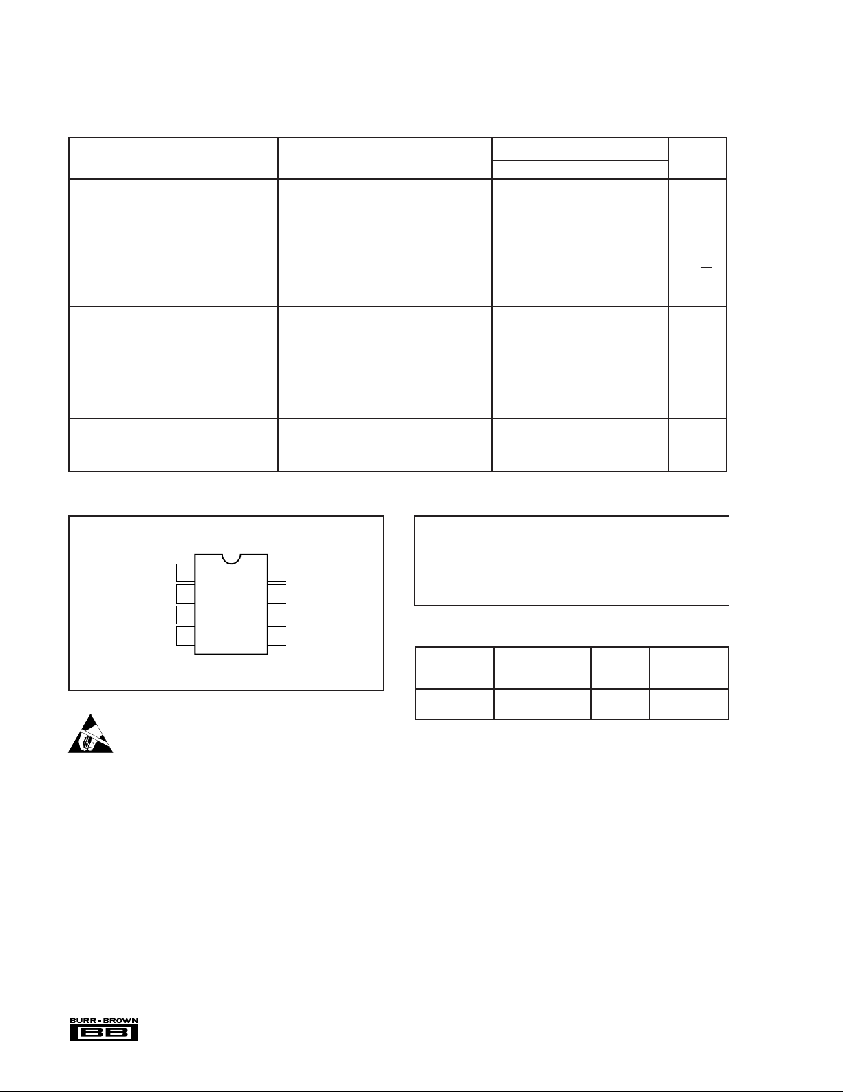
SPECIFICATIONS
ELECTRICAL
At TA = +25°C, VS = 15V, unless otherwise noted.
REF200AP, AU
PARAMETER CONDITION MIN TYP MAX UNITS
CURRENT SOURCES
Current Accuracy ±0.25 ±1%
Current Match ±0.25 ±1%
Temperature Drift Specified Temp Range 25 ppm/°C
Output Impedance 2.5V to 40V 20 100 MΩ
Noise BW = 0.1Hz to 10Hz 1 nAp-p
Voltage Compliance (1%) T
Capacitance 10 pF
CURRENT MIRROR I = 100µA Unless
Gain 0.995 1 1.005
Temperature Drift 25 ppm/°C
Impedance (output) 2V to 40V 40 100 MΩ
Nonlinearity I = 0µA to 250µA 0.05 %
Input Voltage 1.4 V
Output Compliance Voltage See Curves
Frequency Response (–3dB) Transfer 5 MHz
TEMPERATURE RANGE
Specification –25 +85 °C
Operating –40 +85 °C
Storage –40 +125 °C
3.5V to 30V 200 500 MΩ
f = 10kHz 20 pA/√Hz
to T
MIN
MAX
Otherwise Noted
See Curves
PIN CONFIGURATION
Top View DIP/SOIC
I
Low
1
I
Low
2
Mirror Common
Mirror Output
1
2
3
4
8
7
6
5
I
High
1
I
High
2
Substrate
Mirror Input
ELECTROSTATIC
DISCHARGE SENSITIVITY
This integrated circuit can be damaged by ESD. Burr-Brown
recommends that all integrated circuits be handled with
appropriate precautions. Failure to observe proper handling
and installation procedures can cause damage.
ESD damage can range from subtle performance degradation
to complete device failure. Precision integrated circuits may
be more susceptible to damage because very small parametric
changes could cause the device not to meet its published
specifications.
ABSOLUTE MAXIMUM RATINGS
Applied Voltage .....................................................................–6V to +40V
Reverse Current ........................................................................... –350µA
Voltage Between Any Two Sections................................................. ±80V
Operating Temperature ................................................... –40°C to +85°C
Storage Temperature .....................................................–40°C to +125°C
Lead Temperature (soldering, 10s) .............................................. +300°C
(SOIC 3s)........................................................+260°C
PACKAGE/ORDERING INFORMATION
PACKAGE
DRAWING TEMPERATURE
PRODUCT PACKAGE NUMBER
REF200AP 8-Pin Plastic DIP 006 –25°C to +85°C
REF200AU 8-Pin SOIC 182 –25°C to +85°C
NOTE: (1) For detailed drawing and dimension table, please see end of data
sheet, or Appendix C of Burr-Brown IC Data Book. (2) Grade designation “A”
may not be marked. Absence of grade designation indicates A grade.
(1)
RANGE
The information provided herein is believed to be reliable; however, BURR-BROWN assumes no responsibility for inaccuracies or omissions. BURR-BROWN assumes
no responsibility for the use of this information, and all use of such information shall be entirely at the user’s own risk. Prices and specifications are subject to change
without notice. No patent rights or licenses to any of the circuits described herein are implied or granted to any third party. BURR-BROWN does not authorize or warrant
any BURR-BROWN product for use in life support devices and/or systems.
®
REF200
2
TYPICAL PERFORMANCE CURVES
600
500
400
300
200
100
0
5010
Temperature Drift (ppm/°C)
Quantity (Units)
Distribution of three
production lots —
1284 Current Sources.
2015 25 3530 40 5045 55 6560
2
5
117
30
15
6
0
11
501
454
86
66
CURRENT SOURCE
TEMPERATURE DRIFT DISTRIBUTION
1000
900
800
700
600
500
400
300
200
100
Reverse Current (µA)
0
0–2–4–6–8
–10
–12
Reverse Voltage (V)
CURRENT SOURCE
REVERSE CURRENT vs REVERSE VOLTAGE
Reverse Voltage
Circuit Model
12kΩ
7V
5kΩ
Safe Reverse Current
Safe Reverse Voltage
)
At TA = +25°C, VS = +15V, unless otherwise noted.
CURRENT SOURCE
100.1
100
99.9
TYPICAL DRIFT vs TEMPERATURE
99.8
Current (µA)
99.7
99.6
99.5
101
100.8
100.6
100.4
100.2
100
99.8
Current (µA)
99.6
99.4
99.2
99
0 5 10 15 20 25 30 35 40
Drift specified by
“box method”
(See text)
–25–50 25 7550 1251000
Temperature (°C)
CURRENT SOURCE
OUTPUT CURRENT vs VOLTAGE
Voltage (V)
85°C
100.5
100.4
100.3
100.2
100.1
100
99.9
Current (µA)
99.8
99.7
99.6
99.5
0
CURRENT SOURCE
OUTPUT CURRENT vs VOLTAGE
25°C
–55°C
125°C
12345
Voltage (V)
Output Current (500pA/div)
CURRENT SOURCE
CURRENT NOISE (0.1Hz to 10Hz)
Time (500ms/div
®
3
REF200
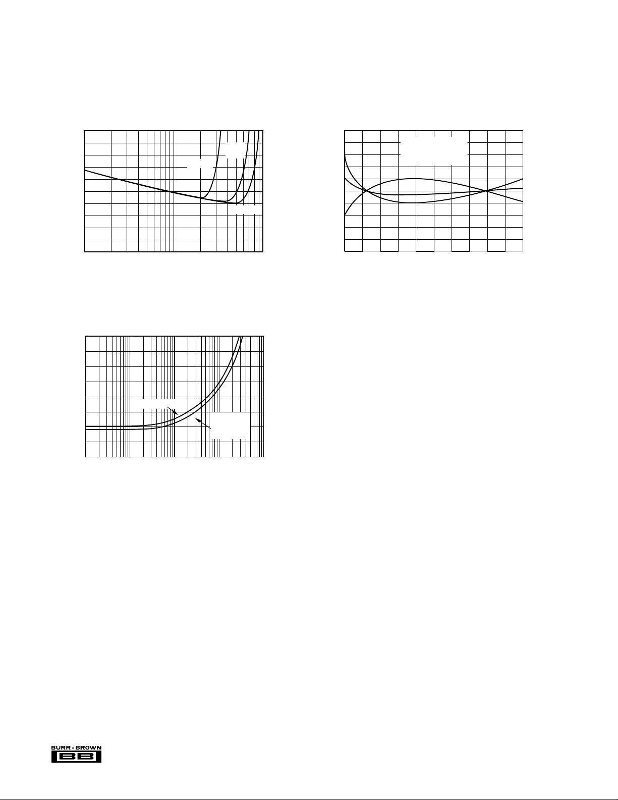
TYPICAL PERFORMANCE CURVES (CONT)
At TA = +25°C, VS = +15V, unless otherwise noted.
5
4
3
2
1
0
Error (%)
–1
–2
–3
–4
–5
10µA 100µA 1mA
4
3
2
Input Voltage (V)
1
MIRROR GAIN ERROR vs CURRENT
V = 1V
O
Mirror Current (A)
MIRROR INPUT VOTAGE/OUTPUT
COMPLIANCE VOLTAGE vs CURRENT
Input Voltage
Output
Compliance
Voltage
V =
O
1.25V
V = 1.5V
O
0.1
0.08
0.06
0.04
0.02
0
–0.02
–0.04
Nonlinearity (% of 250µA)
–0.06
–0.08
–0.01
0
MIRROR TRANSFER NONLINEARITY
50 100 150 200 250
Data from Three
Representative Units
(Least-square fit)
Current (µA)
0
1µA 10µA 100µA
Current
®
REF200
1mA
10mA
4
(Substrate)
Current
Source
(1 of 2)
4kΩ
8X
8,7
5kΩ
1kΩ
1,2
6
3
54
1kΩ
12kΩ
Current
Mirror
APPLICATIONS INFORMATION
The three circuit sections of the REF200 are electrically
isolated from one another using a dielectrically isolated
fabrication process. A substrate connection is provided (pin
6), which is isolated from all circuitry. This pin should be
connected to a defined circuit potential to assure rated DC
performance. The preferred connection is to the most negative constant potential in your system. In most analog
systems this would be –V
pin 6 open and leave unused sections unconnected.
Drift performance is specified by the “box method,” as
illustrated in the Current vs Temperature plot of the typical
performance curves. The upper and lower current extremes
measured over temperature define the top and bottom of the
box. The sides are determined by the specified temperature
range of the device. The drift of the unit is the slope of the
diagonal—typically 25ppm/°C from –25°C to +85°C.
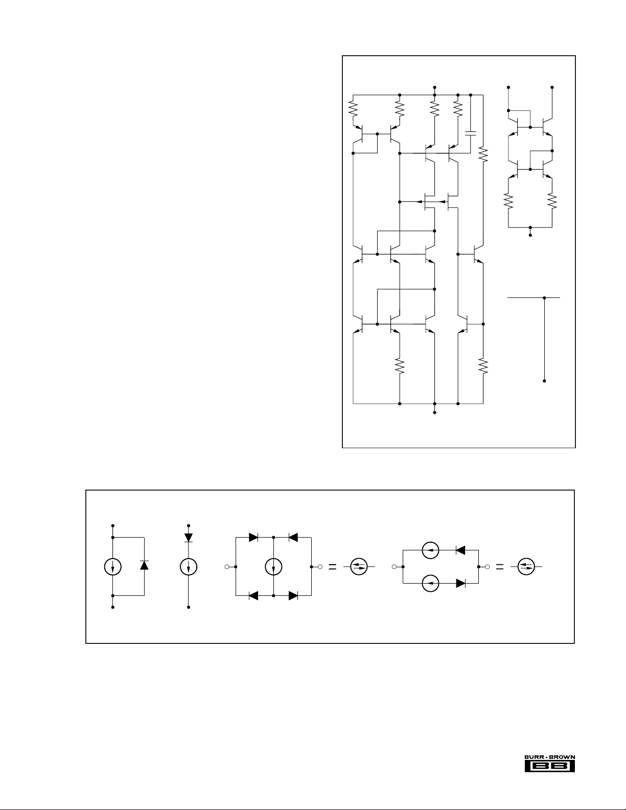
If the current sources are subjected to reverse voltage, a
protection diode may be required. A reverse voltage circuit
model of the REF200 is shown in the Reverse Current vs
Reverse Voltage curve. If reverse voltage is limited to less
than 6V or reverse current is limited to less than 350µA, no
protection circuitry is required. A parallel diode (Figure 2a)
will protect the device by limiting the reverse voltage across
the current source to approximately 0.7V. In some applications, a series diode may be preferable (Figure 2b) because
it allows no reverse current. This will, however, reduce the
compliance voltage range by one diode drop.
Applications for the REF200 are limitless. Application Bulletin AB-165 shows additional REF200 circuits as well as
other related current source techniques. A collection of
circuits is shown to illustrate some techniques. Also, see
AB-165A.
. For best AC performance, leave
S
FIGURE 1. Simplified Circuit Diagram.
(a) (b) (c) (d)
FIGURE 2. Reverse Voltage Protection.
NOTE: All diodes = 1N4148.
DD
D
4
31
100µA
D
2
Bidirectional
Current Source
5
100µA
100µA
D
1
D
2
REF200
Bidirectional
Current Source
®
 Loading...