

Burr Brown RCV420JP, RCV420KP Datasheet
®
RCV420
Precision 4mA to 20mA
CURRENT LOOP RECEIVER
RCV420
FEATURES
● COMPLETE 4-20mA TO 0-5V CONVERSION
● INTERNAL SENSE RESISTORS
● PRECISION 10V REFERENCE
● BUILT-IN LEVEL-SHIFTING
±40V COMMON-MODE INPUT RANGE
●
● 0.1% OVERALL CONVERSION ACCURACY
● HIGH NOISE IMMUNITY: 86dB CMR
DESCRIPTION
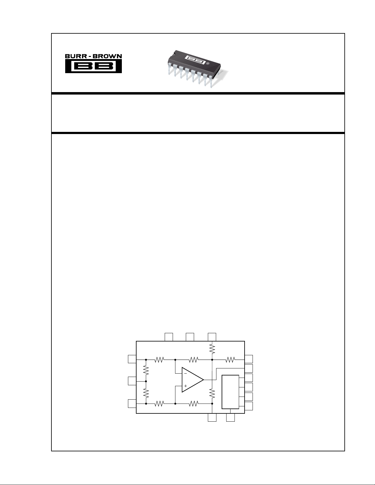
The RCV420 is a precision current-loop receiver designed to convert a 4–20mA input signal into a 0–5V
output signal. As a monolithic circuit, it offers high
reliability at low cost. The circuit consists of a premium grade operational amplifier, an on-chip precision
resistor network, and a precision 10V reference. The
RCV420 features 0.1% overall conversion accuracy,
86dB CMR, and ±40V common-mode input range.
The circuit introduces only a 1.5V drop at full scale,
which is useful in loops containing extra instrument
burdens or in intrinsically safe applications where
APPLICATIONS
● PROCESS CONTROL
● INDUSTRIAL CONTROL
● FACTORY AUTOMATION
● DATA ACQUISITION
● SCADA
● RTUs
● ESD
● MACHINE MONITORING
transmitter compliance voltage is at a premium. The
10V reference provides a precise 10V output with a
typical drift of 5ppm/°C.
The RCV420 is completely self-contained and offers a
highly versatile function. No adjustments are needed
for gain, offset, or CMR. This provides three important
advantages over discrete, board-level designs: 1) lower
initial design cost, 2) lower manufacturing cost, and
3) easy, cost-effective field repair of a precision circuit.
V+ V– Ref In
16 4 12
RCV420
1
–In
2
C
T
+In
3
International Airport Industrial Park • Mailing Address: PO Box 11400, Tucson, AZ 85734 • Street Address: 6730 S. Tucson Blvd., Tucson, AZ 85706 • Tel: (520) 746-1111 • Twx: 910-952-1111
Internet: http://www.burr-brown.com/ • FAXLine: (800) 548-6133 (US/Canada Only) • Cable: BBRCORP • Telex: 066-6491 • FAX: (520) 889-1510 • Immediate Product Info: (800) 548-6132
©
1988 Burr-Brown Corporation PDS-837E Printed in U.S.A. October, 1997
300kΩ
RS
75Ω
R
75Ω
300kΩ
S
99kΩ
1.01kΩ
100kΩ
1
92kΩ
13 5
Rcv
Com
11.5kΩ
+10V
Ref
Ref
Com
15
14
11
10
Rcv f
B
Rcv Out
Ref Out
Ref f
B
Ref Trim
8
Ref Noise Reduction
7
®
RCV420

SPECIFICATIONS
ELECTRICAL
At T = +25°C and VS = ±15V, unless otherwise noted.
RCV420KP, JP
CHARACTERISTICS MIN TYP MAX UNITS
GAIN
Initial 0.3125 V/mA
Error 0.05 0.15 % of span
Error—JP Grade 0.25 % of span
vs Temp 15 ppm/°C
Nonlinearity
OUTPUT
Rated Voltage (I
Rated Current (E
Impedance (Differential) 0.01 Ω
Current Limit (To Common) +49, –13 mA
Capacitive Load 1000 pF
INPUT
Sense Resistance 74.25 75 75.75 Ω
Input Impedance (Common-Mode) 200 kΩ
Common-Mode Voltage ±40 V
CMR
AC 60Hz 80 dB
OFFSET VOLTAGE (RTO)
Initial 1mV
ZERO ERROR
Initial 0.025 0.075 % of span
Initial—JP Grade 0.15 % of span
OUTPUT NOISE VOLTAGE
f
B
f
O
DYNAMIC RESPONSE
Gain Bandwidth 150 kHz
Full Power Bandwidth 30 kHz
Slew Rate 1.5 V/µs
Settling Time (0.01%) 10 µs
VOLTAGE REFERENCE
Initial 9.99 10.01 V
Trim Range
Noise (0.1Hz to 10Hz) 5 µVp-p
Output Current +10, –2 mA
POWER SUPPLY
Rated ±15 V
Voltage Range
Quiescent Current (V
TEMPERATURE RANGE
Specification 0 +70 °C
Operation –25 +85 °C
Storage –40 +85 °C
Thermal Resistance,
NOTES: (1) Nonlinearity is the max peak deviation from best fit straight line. (2) With 0 source impedance on Rcv Com pin. (3) Referred to output with all inputs
grounded including Ref In. (4) With 4mA input signal and Voltage Reference connected (includes V
slightly affects drift. (6) I
(1)
= +10mA, –5mA) 10 12 V
O
= 10V) +10, –5 mA
O
0.0002 0.002 % of span
(Stable Operation)
(2)
vs Temp (DC) (T
A
= T
MIN
to T
)76dB
MAX
(3)
70 80 dB
vs Temp 10 µV/°C
vs Supply (±11.4V to ±18V) 74 90 dB
vs Time 200 µV/mo
(4)
vs Temp 10 ppm of
span/°C
= 0.1Hz to 10Hz 50 µVp-p
= 10kHz 800 nV/√Hz
(5)
±4%
vs Temp 5 ppm/°C
vs Supply (±11.4V to ±18V) 0.0002 %/V
vs Output Current (I
vs Time 15 ppm/kHz
= 0 to +10mA) 0.0002 %/mA
O
(6)
= 0V) 3 4 mA
O
θ
JA
Ref = 5mA, IO Rcv = 2mA.
O
–5, +11.4 ±18 V
80 °C/W
, Gain Error, and Voltage Reference Errors). (5) External trim
OS
®
RCV420
2
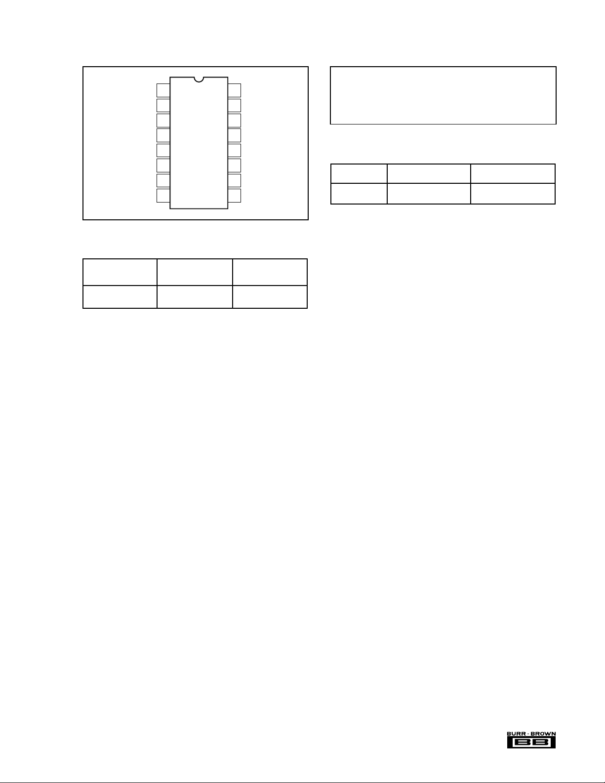
PIN CONFIGURATION
Top View DIP
–In
C
+In
V–
Ref Com
NC
Ref Noise Reduction
Ref Trim
1
2
T
3
4
5
6
7
8
16
15
14
13
12
11
10
9
V+
Rcv f
B
Rcv Out
Rcv Com
Ref In
Ref Out
Ref f
B
NC
ORDERING INFORMATION
ABSOLUTE MAXIMUM RATINGS
Supply ...............................................................................................±22V
Input Current, Continuous ................................................................ 40mA
Input Current Momentary, 0.1s ........................... 250mA, 1% Duty Cycle
Common-Mode Input Voltage, Continuous ....................................... ±40V
Lead Temperature (soldering, 10s)............................................... +300°C
Output Short Circuit to Common (Rcv and Ref) ..................... Continuous
NOTE: (1) Stresses above these ratings may cause permanent damage.
(1)
PACKAGE INFORMATION
PRODUCT PACKAGE NUMBER
RCV420KP 16-Pin Plastic DIP 180
RCV420JP 16-Pin Plastic DIP 180
NOTE: (1) For detailed drawing and dimension table, please see end of data
sheet, or Appendix C of Burr-Brown IC Data Book.
PACKAGE DRAWING
(1)
PRODUCT GRADE PACKAGE
RCV420KP 0°C to +70°C 16-Pin Plastic DIP
RCV420JP 0°C to +70°C 16-Pin Plastic DIP
PERFORMANCE
The information provided herein is believed to be reliable; however, BURR-BROWN assumes no responsibility for inaccuracies or omissions. BURR-BROWN assumes
no responsibility for the use of this information, and all use of such information shall be entirely at the user’s own risk. Prices and specifications are subject to change
without notice. No patent rights or licenses to any of the circuits described herein are implied or granted to any third party. BURR-BROWN does not authorize or warrant
any BURR-BROWN product for use in life support devices and/or systems.
3
RCV420
®
 Loading...