

Burr Brown PLL1700E, PLL1700E-2K Datasheet
49%
FPO
PLL1700
®
International Airport Industrial Park • Mailing Address: PO Box 11400, Tucson, AZ 85734 • Street Address: 6730 S. Tucson Blvd., Tucson, AZ 85706 • Tel: (520) 746-1111 • Twx: 910-952-1111
Internet: http://www.burr-brown.com/ • FAXLine: (800) 548-6133 (US/Canada Only) • Cable: BBRCORP • Telex: 066-6491 • FAX: (520) 889-1510 • Immediate Product Info: (800) 548-6132
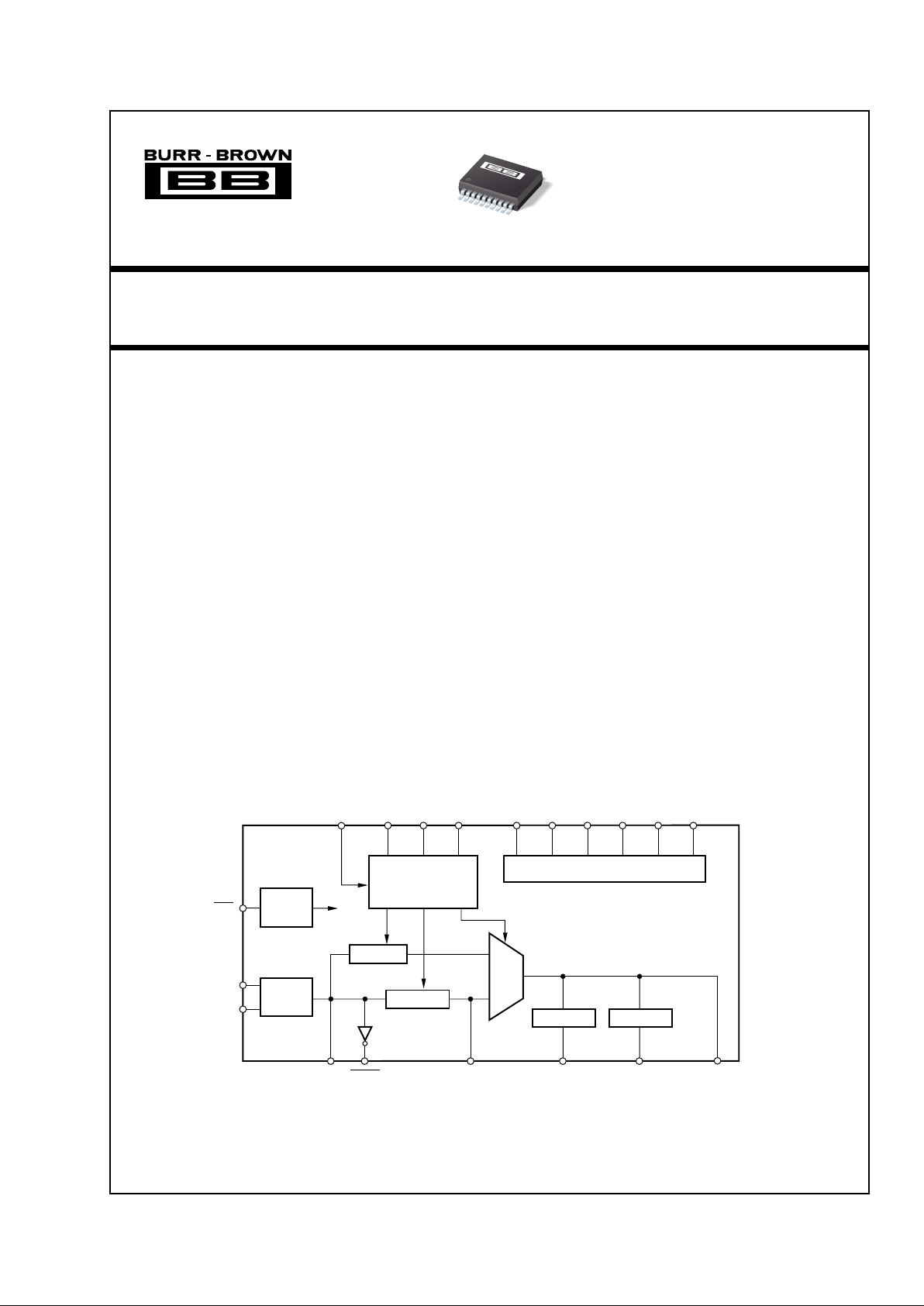
MULTI-CLOCK GENERATOR
DESCRIPTION
The PLL1700 is a low cost, multi-clock generator
Phase Lock Loop (PLL).
The PLL1700 can generate four systems clocks from a
27MHz reference input frequency.
The device gives customers both cost and space savings
by eliminating external components and enables customers to achive the very low jitter performance needed
for high performance audio digital-to-analog converters (DAC) and/or analog-to-digital converters (ADC).
The PLL1700 is ideal for MPEG-2 applications which
use a 27MHz master clock such as DVD players, DVD
add-on cards for multimedia PCs, digital HDTV systems, and set-top boxes.
FEATURES
● 27MHZ MASTER CLOCK INPUT
● GENERATED AUDIO SYSTEM CLOCK:
SCKO1: 33.8688MHz (Fixed)
SCKO2: 256f
S
SCKO3: 384f
S
SCKO4: 768f
S
● ZERO PPM ERROR OUTPUT CLOCKS
● LOW CLOCK JITTER: 150ps at SCKO3
● MULTIPLE SAMPLING FREQUENCIES:
fS = 32kHz, 44.1kHz, 48kHz, 64kHz,
88.2kHz, 96kHz
● +3.3V CMOS LOGIC INTERFACE
● DUAL POWER SUPPLIES: +5V and +3.3V
● SMALL PACKAGE: 20-Lead SSOP
OSC
PLL2
PLL1
Counter Q
Counter P
SCKO2
SCKO3 SCKO4
MCKOMCKO
XT1
XT2
Reset
Mode
Control
I/F
Power Supply
RST
MODE ML MC MD V
DDP
V
DDB
V
DD
GNDP GNDB GND
SCKO1
© 1998 Burr-Brown Corporation PDS-1455A Printed in U.S.A. August, 1998
®
PLL1700
®
2
PLL1700
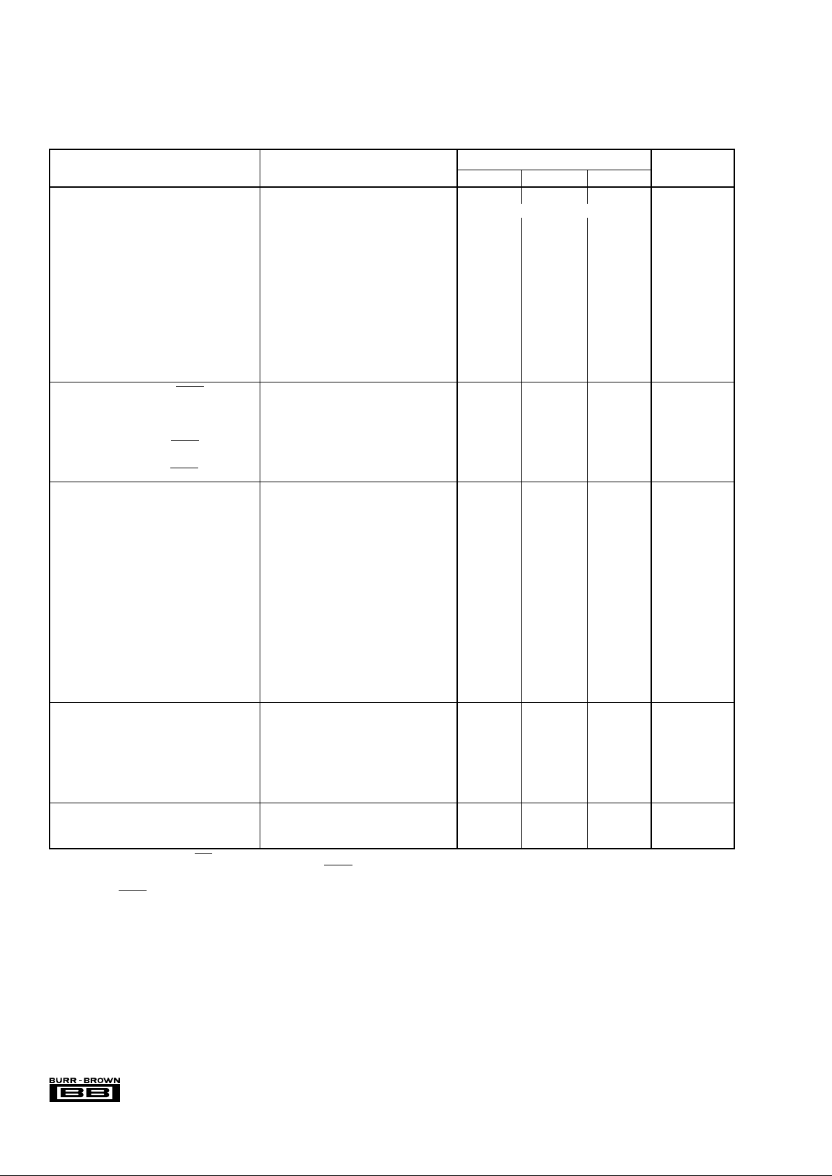
SPECIFICATIONS
All specifications at TA = +25°C, VDD = V
DDP
= +5V, V
DDB
= +3.3V, fM = 27MHz crystal oscillation and fS = 48kHz, unless otherwise noted.
The information provided herein is believed to be reliable; however, BURR-BROWN assumes no responsibility for inaccuracies or omissions. BURR-BROWN assumes
no responsibility for the use of this information, and all use of such information shall be entirely at the user’s own risk. Prices and specifications are subject to change
without notice. No patent rights or licenses to any of the circuits described herein are implied or granted to any third party. BURR-BROWN does not authorize or warrant
any BURR-BROWN product for use in life support devices and/or systems.
PLL1700E
PARAMETER CONDITIONS MIN TYP MAX UNITS
DIGITAL INPUT/OUTPUT
Input Logic Level: TTL-Compatible
V
IH
2.0 VDC
V
IL
0.8 VDC
Input Logic Current:
I
IH
(1)
VIN = V
DD
200 µA
I
IL
(1)
VIN = 0V –1 µA
I
IH
(2)
VIN = V
DD
4mA
I
IL
(2)
VIN = 0V –800 µA
Output Logic Level: CMOS
V
OH
(3)
IOH = 4mA V
DDB
– 0.4V VDC
V
OL
(3)
IOL = 4mA 0.4 VDC
Sampling Frequency (fS) Standard f
S
32 44.1 48 kHz
Double f
S
64 88.2 96 kHz
MASTER CLOCK (MCKO, MCKO) f
M
= 27MHz, CL = 20pF
Master Clock Frequency 26.73 27 27.27 MHz
Clock Jitter
(4)
300 ps
Clock Duty Cycle MCKO 40 50 60 %
For Crystal Oscillation MCKO 40 50 60 %
Clock Duty Cycle MCKO 40 %
For External Clock MCKO 60 %
PHASE LOCK LOOP (PLL) f
M
= 27MHz, CL = 20pF
Generated System Clock Frequency
SCKO1 Fixed 33.8688 MHz
SCKO2 256f
S
8.192 24.576 MHz
SCKO3 384f
S
12.288 36.864 MHz
SCKO4 768f
S
24.576 36.864 MHz
Generated Clock Rise Time
(3)
20% to 80% V
DDB
5ns
Generated Clock Fall Time
(3)
80% to 20% V
DDB
5ns
Generated Clock Duty Cycle SCKO1, SCKO3, SCKO4 40 50 60 %
SCKO2 (standard) 40 50 60 %
SCKO2 (double)
(5)
25 33 40 %
Generated Clock Jitter
(4)
SCKO1, SCKO2 (standard), SCKO4 300 ps
SCKO3 150 ps
SCKO2 (double) 450 ps
Settling Time To Programmed Frequency 20 ms
Power-Up Time To Programmed Frequency 15 30 ms
POWER SUPPLY REQUIREMENTS
Voltage Range V
DD
, V
DDP
+4.5 +5 +5.5 VDC
V
DDB
+2.7 +3.3 +3.6 VDC
Supply Current
(6)
:
I
DD
+ I
DDP
VDD = V
DDP
= 5V, fS = 48kHz 11 16 mA
I
DDB
V
DDB
= +3.3V, fS = 48kHz 6 9 mA
Power Dissipation f
S
= 48kHz 75 110 mW
TEMPERATURE RANGE
Operation –25 +85 °C
Storage –55 +125 °C
NOTES: (1) ML, MC, MD, MODE, RST (Schmitt-trigger input with internal pull-down resistor). (2) XT1, when an external 27MHz clock is used, the buffer ICs, such
as 74HC04, are recommended to interface to XT1. (3) MCKO, MCKO, SCKO4, SCKO3, SCKO2, and SCKO1. (4) Jitter performance is specified as standard
deviation of jitter under 27MHz crystal oscillation. (5) When SCKO2 is set to double rate clock output, its duty cycle is 33%. (6) f
M
= 27MHz crystal oscillation, no
load on MCKO, MCKO, SCKO4, SCKO3, SCKO2, and SCKO1.
®
3
PLL1700
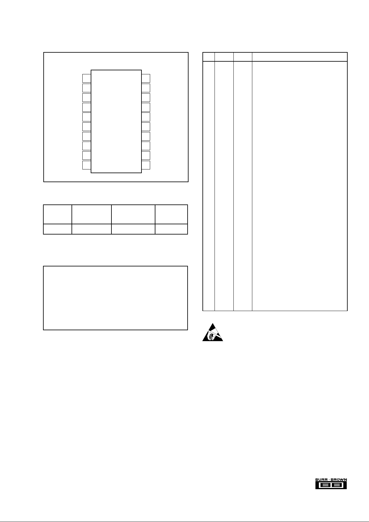
PIN ASSIGNMENTS
PIN CONFIGURATION
TOP VIEW SSOP
PACKAGE INFORMATION
PACKAGE
TEMPERATURE DRAWING
PRODUCT PACKAGE RANGE NUMBER
(1)
PLL1700E 20-Lead SSOP –25°C to +85°C 334-1
NOTE: (1) For detailed drawing and dimension table, please see end of data
sheet, or Appendix C of Burr-Brown IC Data Book.
ABSOLUTE MAXIMUM RATINGS
Supply Voltage (+VDD, +V
DDP
, +V
DDB
) .............................................. +6.5V
Supply Voltage Differences (+V
DD
, +V
DDP
) ....................................... ±0.1V
GND Voltage Differences: GND, GNDP, GNDB............................... ±0.1V
Digital Input Voltage................................................. –0.3V to (V
DD
+ 0.3V)
Digital Output Voltage ............................................ –0.3V to (V
DDB
+ 0.3V)
Input Current (any pins except supply pins) ................................... ±10mA
Power Dissipation .......................................................................... 300mW
Operating Temperature Range ......................................... –25°C to +85°C
Storage Temperature...................................................... –55°C to +125°C
Lead Temperature (soldering, 5s) ................................................. +260°C
Package Temperature (IR reflow, 10s) .......................................... +235°C
PIN NAME I/O FUNCTION
1 ML/SR0 IN Latch Enable for Software Mode/Sampling Rate
Selection for Hardware Mode. When MODE pin
is LOW, ML is selected.
(1)
2 MODE IN Mode Control Select. When this pin is HIGH,
device is operated in hardware mode using SR0
(pin 1), FS0 (pin 19), and FS1 (pin 20). When
this pin is LOW, device is operated in software
mode by three-wire interface using ML (pin 1),
MD (pin 19) and MC (pin 20).
(1)
3VDD— Digital Power Supply, +5V.
4 GND — Digital Ground.
5 XT2 — 27MHz Crystal. When an external 27MHz clock
is applied to XT1 (pin 6), this pin must be
connected to GND.
6 XT1 IN 27MHz Oscillator Input/External 27MHz Input.
7 GNDP — Ground for PLL.
8V
DDP
— Power Supply for PLL, +5V.
9 RSV — Reserved. Must be left open.
10 MCKO OUT 27MHz Output.
11 MCKO OUT Inverted 27MHz Output.
12 SCKO1 OUT Fixed 33.8688MHz Clock Output.
13 SCKO4 OUT 768f
S
Clock Output.
14 SCKO2 OUT 256f
S
Clock Output.
15 GNDB — Digital Ground for V
DDB
.
16 V
DDB
— Digital Power Supply for Clock Output Buffers,
+3.3V.
17 SCKO3 OUT 384f
S
Output. This output has been optimized
for the lowest jitter and should be connected to
the audio DAC(s).
18 RST IN Reset. When this pin is LOW, device is held in
reset.
(1)
19 MD/FS0 IN Serial Data Input for Software Mode/Sampling
Frequency Selection for Hardware Mode. When
MODE pin is LOW, MD is selected.
(1)
20 MC/FS1 IN Shift Clock Input for Software Mode/Sampling
Frequency Selection for Hardware Mode. When
MODE pin is LOW, MC is selected.
(1)
NOTE: (1) Schmitt-trigger input with internal pull-down resistors.
ELECTROSTATIC
DISCHARGE SENSITIVITY
This integrated circuit can be damaged by ESD. Burr-Brown
recommends that all integrated circuits be handled with
appropriate precautions. Failure to observe proper handling
and installation procedures can cause damage.
ESD damage can range from subtle performance degradation
to complete device failure. Precision integrated circuits may
be more susceptible to damage because very small parametric
changes could cause the device not to meet its published
specifications.
ML/SR0
MODE
V
DD
GND
XT2
XT1
GNDP
V
DDP
RSV
MCKO
MC/FS1
MD/FS0
RST
SCKO3
V
DDB
GNDB
SCKO2
SCKO4
SCKO1
MCKO
1
2
3
4
5
6
7
8
9
10
20
19
18
17
16
15
14
13
12
11
PLL1700E
 Loading...