

Burr Brown PGA206PA, PGA206UA, PGA207PA, PGA207UA, PGA207UA-1K Datasheet
©
1994 Burr-Brown Corporation PDS-1241B Printed in U.S.A. May, 1995
A
1
A
2
A
3
12
11
10
10kΩ10kΩ
10kΩ10kΩ
13
7
5
14
16
4
V
IN
V
IN
V+
PGA206
PGA207
Ref
V
O
–
+
Over-Voltage
Protection
Over-Voltage
Protection
Feedback
Digitally Selected
Feedback Network
1
V
O1
15
A
1
A
0
Digital
Ground
6 9 8
V
O2
V–V
OS
Adj
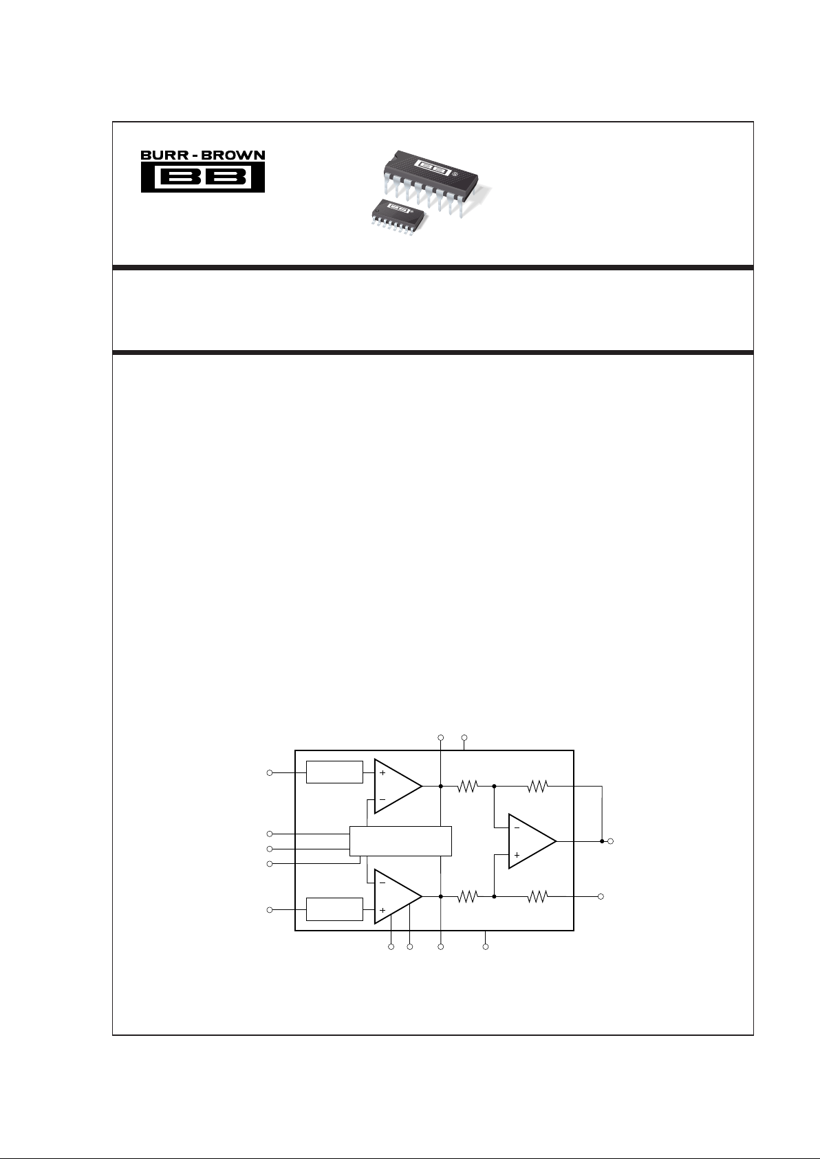
High-Speed Programmable Gain
INSTRUMENTATION AMPLIFIER
FEATURES
● DIGITALLY PROGRAMMABLE GAINS:
PGA206: G=1, 2, 4, 8V/V
PGA207: G=1, 2, 5, 10V/V
● TRUE INSTRUMENTATION AMP INPUT
● FAST SETTLING: 3.5
µs to 0.01%
● FET INPUT: I
B
= 100pA max
● INPUT PROTECTION:
±40V
● LOW OFFSET VOLTAGE: 1.5mV max
● 16-PIN DIP, SOL-16 SOIC PACKAGES
APPLICATIONS
● MULTIPLE-CHANNEL DATA ACQUISITION
● MEDICAL, PHYSIOLOGICAL AMPLIFIER
● PC-CONTROLLED ANALOG INPUT
BOARDS
DESCRIPTION
The PGA206 and PGA207 are digitally programmable
gain instrumentation amplifiers that are ideally suited
for data acquisition systems.
The PGA206 and PGA207’s fast settling time allows
multiplexed input channels for excellent system efficiency. FET inputs eliminate I
B
errors due to analog
multiplexer series resistance.
Gains are selected by two CMOS/TTL-compatible
address lines. Analog inputs are internally protected
for overloads up to ±40V, even with the power supplies off. The PGA206 and PGA207 are laser-trimmed
for low offset voltage and low drift.
The PGA206 and PGA207 are available in 16-pin
plastic DIP and SOL-16 surface-mount packages. Both
are specified for –40°C to +85°C operation.
PGA206
PGA207
®
International Airport Industrial Park • Mailing Address: PO Box 11400, Tucson, AZ 85734 • Street Address: 6730 S. Tucson Blvd., Tucson, AZ 85706 • Tel: (520) 746-1111 • Twx: 910-952-1111
Internet: http://www.burr-brown.com/ • FAXLine: (800) 548-6133 (US/Canada Only) • Cable: BBRCORP • Telex: 066-6491 • FAX: (520) 889-1510 • Immediate Product Info: (800) 548-6132
PGA206
PGA207
2
®
PGA206/207
PGA206P, U PGA206PA, UA
PGA207P, U PGA207PA, UA
PARAMETER CONDITIONS MIN TYP MAX MIN TYP MAX UNITS
SPECIFICATIONS
At TA = +25°C, VS = ±15V, RL = 2kΩ unless otherwise noted.
The information provided herein is believed to be reliable; however, BURR-BROWN assumes no responsibility for inaccuracies or omissions. BURR-BROWN assumes
no responsibility for the use of this information, and all use of such information shall be entirely at the user’s own risk. Prices and specifications are subject to change
without notice. No patent rights or licenses to any of the circuits described herein are implied or granted to any third party. BURR-BROWN does not authorize or warrant
any BURR-BROWN product for use in life support devices and/or systems.
INPUT
Offset Voltage, RTI All Gains
Initial T
A
= +25°C ±0.5 ±1.5 ±1 ±2.5 mV
vs Temperature T
A
= T
MIN
to T
MAX
, G = 8, 10 ±2 ✻ µV/°C
vs Power Supply V
S
= ±4.5V to ±18V ±5 ±20 ±10 ±40 µV/V
Long-Term Stability 4.5 ✻ µV/mo
Impedance, Differential 10
13
|| 1 ✻ Ω || pF
Common-Mode 10
12
|| 4 ✻ Ω || pF
Common-Mode Voltage Range
(1)
VO = 0V ±(|VS|–4) ±(|VS| –2.5) ✻✻ V
Safe Input Voltage ±40 ✻ V
Common-Mode Rejection V
CM
= ±11V, ∆RS = 1kΩ
G = 1 80 92 75 86 dB
G = 2 85 96 80 90 dB
G = 4 or 5 90 100 84 94 dB
G = 8 or 10 95 100 84 94 dB
INPUT BIAS CURRENT V
IN
= 0 2 100 ✻✻pA
vs Temperature See Typical Curve ✻
Offset Current 1 100 ✻✻pA
vs Temperature See Typical Curve ✻
NOISE VOLTAGE, RTI G = 8,10; R
S
= 0Ω
f = 10Hz 30 ✻ nV/√Hz
f = 100Hz 20 ✻ nV/√Hz
f = 1kHz 18 ✻ nV/√Hz
f
B
= 0.1Hz to 10Hz 1 ✻ µVp-p
Noise Current
f = 1kHz 1.5 ✻ fA/√Hz
GAIN
All Gains, VO = ±11V
Gain Error ±0.01 ±0.05 ✻ ±0.1 %
Gain vs Temperature
(2)
±1 ±10 ✻✻ppm/°C
Nonlinearity ±0.0003 ±0.002 ✻ ±0.005 % of FSR
OUTPUT
Voltage, Positive (V+) –4 (V+) –2.3 ✻✻ V
Negative (V–) +4 (V–) +1.5 ✻✻ V
Load Capacitance Stability 1000 ✻ pF
Short-Circuit Current ±17 ✻ mA
FREQUENCY RESPONSE
Bandwidth, –3dB G = 1 5 ✻ MHz
G = 2 4 ✻ MHz
G = 4, 5 1.3 ✻ MHz
G = 8, 10 600 ✻ kHz
Slew Rate V
O
= ±10V, G = 1 to 10 25 ✻ V/µs
Settling Time, 0.1% 20V Step, All Gains 2 ✻ µs
0.01% 20V Step, All Gains 3.5 ✻ µs
Output Overload Recovery 50% Overdrive 1.5 ✻ µs
DIGITAL LOGIC INPUTS
Digital Ground Voltage, V
DG
V– (V+) –4 ✻✻V
Digital Low Voltage V– V
DG
+ 0.8V ✻✻V
Digital Input Current 1 ✻ pA
Digital High Voltage V
DG
+2 V+ ✻✻V
Gain Switching Time 500 ✻ ns
POWER SUPPLY
Voltage Range ±4.5 ±15 ±18 ✻✻ ✻ V
Current V
IN
= 0V +12.4/–11.2 ±13.5 ✻ mA
TEMPERATURE RANGE
Specification –40 +85 ✻✻°C
Operating –40 +125 ✻✻°C
Thermal Resistance,
θ
JA
80 ✻ °C/W
✻ Specification same as PGA206P or PGA207P.
NOTES: (1) Input common-mode range varies with output voltage—see typical curves. (2) Guaranteed by wafer test.
3
®
PGA206/207
TEMPERATURE
PRODUCT GAINS PACKAGE RANGE
PGA206PA 1, 2, 4, 8V/V 16-Pin Plastic DIP –40°C to +85°C
PGA206P 1, 2, 4, 8V/V 16-Pin Plastic DIP –40°C to +85°C
PGA206UA 1, 2, 4, 8V/V SOL-16 Surface-Mount –40°C to +85°C
PGA206U 1, 2, 4, 8V/V SOL-16 Surface-Mount –40°C to +85°C
PGA207PA 1, 2, 5, 10V/V 16-Pin Plastic DIP –40°C to +85°C
PGA207P 1, 2, 5, 10V/V 16-Pin Plastic DIP –40°C to +85°C
PGA207UA 1, 2, 5, 10V/V SOL-16 Surface-Mount –40°C to +85°C
PGA207U 1, 2, 5, 10V/V SOL-16 Surface-Mount –40°C to +85°C
ABSOLUTE MAXIMUM RATINGS
Supply Voltage .................................................................................. ±18V
Analog Input Voltage Range ............................................................. ±40V
Logic Input Voltage Range.................................................................. ±V
S
Output Short-Circuit (to ground) .............................................. Continuous
Operating Temperature ................................................. –40°C to +125°C
Storage Temperature ..................................................... –40°C to +125°C
Junction Temperature .................................................................... +150°C
Lead Temperature (soldering –10s).............................................. +300°C
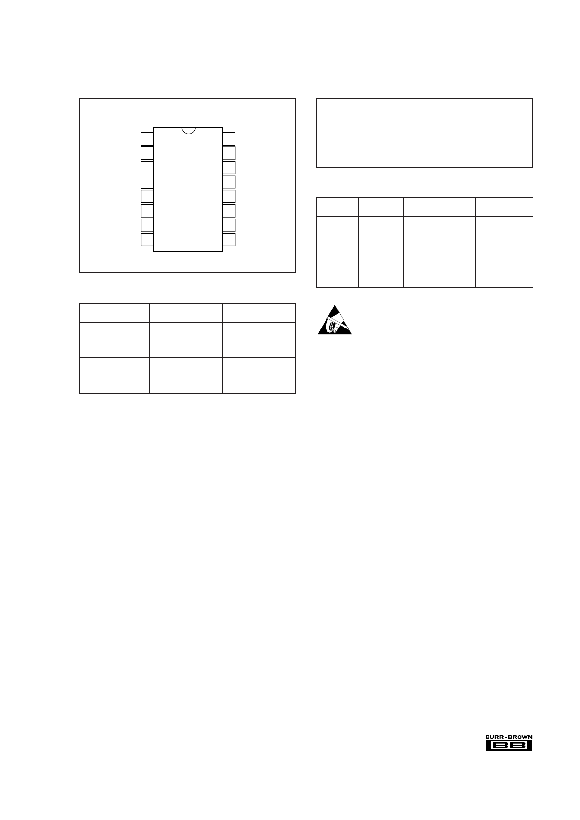
ORDERING INFORMATION
ELECTROSTATIC
DISCHARGE SENSITIVITY
This integrated circuit can be damaged by ESD. Burr-Brown
recommends that all integrated circuits be handled with appropriate precautions. Failure to observe proper handling and
installation procedures can cause damage.
ESD damage can range from subtle performance degradation
to complete device failure. Precision integrated circuits may
be more susceptible to damage because very small parametric
changes could cause the device not to meet its published
specifications.
PIN CONFIGURATION
Top View DIP
SOL-16
V
O1
NC
NC
V
IN
V
IN
V
OS
Adjust
V
OS
Adjust
V–
A
1
A
0
Dig. Ground
V+
Sense
V
O
Ref
V
O2
1
2
3
4
5
6
7
8
16
15
14
13
12
11
10
9
–
+
NC: No Internal Connection
PACKAGE INFORMATION
PACKAGE DRAWING
PRODUCT PACKAGE NUMBER
(1)
PGA206PA 16-Pin Plastic DIP 180
PGA206P 16-Pin Plastic DIP 180
PGA206UA SOL-16 Surface Mount 211
PGA206U SOL-16 Surface Mount 211
PGA207PA 16-Pin Plastic DIP 180
PGA207P 16-Pin Plastic DIP 180
PGA207UA SOL-16 Surface Mount 211
PGA207U SOL-16 Surface Mount 211
NOTE: (1) For detailed drawing and dimension table, please see end of data
sheet, or Appendix C of Burr-Brown IC Data Book.
 Loading...