

Burr Brown PCM78P Datasheet
®
PCM78P
16-Bit Audio
ANALOG-TO-DIGITAL CONVERTER
FEATURES
● LOW COST/HIGH PERFORMANCE 16-BIT
AUDIO A/D CONVERTER
● FAST 5
(4
µs MAX CONVERSION TIME
µs typ)
● VERY LOW THD+N ( typ –88dB at FS;
max –82dB)
±3V INPUT RANGE
●
● TWO SERIAL OUTPUT MODES PROVIDE
VERSATILE INTERFACING
● COMPLETE WITH INTERNAL REFERENCE
AND CLOCK IN 28-PIN PLASTIC DIP
±5V TO ±15V SUPPLY RANGE (600mW
●
Power Dissipation)
DESCRIPTION
The PCM78P is a low-cost 16-bit analog-to-digital
converter which is specifically designed and tested for
dynamic applications. It features very fast, low
distortion performance (4µs/–88dB THD+N typical)
and is complete with internal clock and reference
circuitry. The PCM78P is packaged in a reliable, lowcost 28-pin plastic DIP and data output is available in
user-selectable serial output formats. The PCM78P is
ideal for digital audio tape (DAT) recorders. Many
similar applications such as digital signal processing
and telecom applications are equally well served by
the PCM78P.
The PCM78P uses a SAR technique. Analog and
digital portions are efficiently partitioned into a highspeed, bipolar section and a low-power CMOS
section. The PCM78P has been optimized for excellent dynamic performance and low cost.
APPLICATIONS
● DSP DATA ACQUISITION
● TEST INSTRUMENTATION
● SAMPLING KEYBOARD SYNTHESIZERS
● DIGITAL AUDIO TAPE
● BROADCAST AUDIO PROCESSING
● TELECOMMUNICATIONS
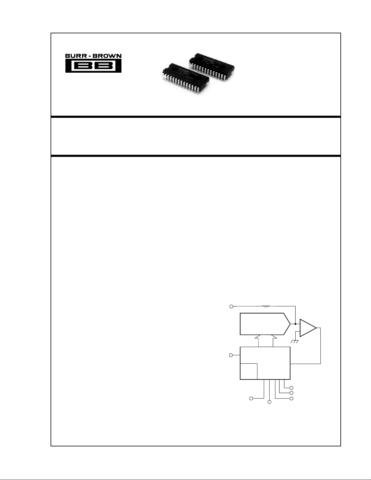
Audio Input
Convert
Command
External Clock
16-bit D/A
Converter
16-bit SAR +
Timing Control
Internal
Clock
Circuit
Status
–
Comp
+
Serial Output 1
Serial Output 2
Clock Output
International Airport Industrial Park • Mailing Address: PO Box 11400 • Tucson, AZ 85734 • Street Address: 6730 S. Tucson Blvd. • Tucson, AZ 85706
Tel: (520) 746-1111 • Twx: 910-952-1111 • Cable: BBRCORP • Telex: 066-6491 • FAX: (520) 889-1510 • Immediate Product Info: (800) 548-6132
©
1989 Burr-Brown Corporation PDS-989A Printed in U.S.A. October, 1993
SPECIFICATIONS
ELECTRICAL
At TC = +25°C, +V
PARAMETER CONDITIONS MIN TYP MAX UNITS
RESOLUTION 16 Bits
INPUT/OUTPUT
ANALOG INPUT
Input Range –3 +3 V
Input Impedance 1.5 kΩ
DIGITAL INPUT/OUTPUT
Logic Family TTL Compatible CMOS
Logic Level: V
Data Format Serial BOB or BTC
Convert Command Negative Edge
Pulse Width 25 50 ns
CONVERSION TIME 45 µs
DYNAMIC CHARACTERISTICS
SIGNAL-TO-NOISE RATIO (SNR)
f = 1kHz (0dB) BW = 20kHz 90 dB
f = 10kHz (0dB) BW = 100kHz 80 dB
TOTAL HARMONIC DISTORTION
f = 1kHz (0dB) BW = 20kHz –91 dB
f = 19kHz (0dB) BW = 20kHz –90 dB
f = 10kHz (0dB) BW = 100kHz –90 dB
f = 90kHz (0dB) BW = 100kHz –89 dB
TOTAL HARMONIC DISTORTION + NOISE
f = 1kHz (0dB) BW = 20kHz –88 –82 dB
f = 1kHz (–20dB) BW = 20kHz –74 –68 dB
f = 1kHz (–60dB) BW = 20kHz –34 dB
f = 19kHz (0dB) BW = 20kHz –87 dB
f = 10kHz (0dB) BW = 100kHz –82 dB
f = 90kHz (0dB) BW = 100kHz –81 dB
TRANSFER CHARACTERISTICS
ACCURACY
Gain Error ±2%
Bipolar Zero Error ±20 mV
Differential Linearity Error ±0.002 % of FSR
Integral Linearity Error ±0.003 % of FSR
Missing Codes None 14 Bits
DRIFT
Gain 0°C to +70°C ±25 ppm/°C
Bipolar Zero 0°C to +70°C ±4 ppm of FSR/°C
POWER SUPPLY SENSITIVITY
+V
CC
–V
CC
+V
DD
POWER SUPPLY REQUIREMENTS
Voltage Range: +V
Current: +V
Power Dissipation ±V
TEMPERATURE RANGE
Specification 0 +70 °C
Storage –50 +100 °C
Operating –25 +85 °C
= +5V, and ±VCC = ±12V, and one minute warm-up in convection environment, unless otherwise noted.
DD
IH
V
IL
V
OH
V
OL
(2)
(5)
(6)
CC
–V
CC
+V
DD
CC
–V
CC
+V
DD
IIH = +40µA +2 +5.5 V
IIL = –100µA 0 +0.8 V
IOH = 2TTL Loads +2.4 V
IOL = 2TTL Loads +0.4 V
CONV
CONV
= 4µs
= 4µs
= 4µs
(3)
fS = 200kHz/T
fS = 200kHz/T
fS = 200kHz/T
CONV
+4.75 +15.6 V
–4.75 –15.6 V
+4.75 +5.25 V
+VCC = +12V +15 mA
–VCC = –12V –21 mA
+VDD = +5V +7 mA
= ±12V 575 mW
CC
PCM78P
(1)
±0.008 %FSR/%V
±0.003 %FSR/%V
±0.003 %FSR/%V
(4)
(7)
(8)
CC
CC
DD
NOTES: (1) When convert command is high, converter is in a halt/reset mode. Actual conversion begins on negative edge. See detailed text on timing for convert
command description when using external clock. (2) Ratio of Noise rms/Signal rms. (3) f = input frequency; f
combination); BW = bandwidth of output (based on FFT or actual analog reconstruction using a 20kHz low-pass filter). (4) Referred to input signal level. (5) Ratio
= sample frequency (PCM78P and SHC702 in
S
of Distortion rms/Signal rms. (6) Ratio of Distortion rms + Noise rms/Signal rms. (7) FSR: Full-Scale Range = 6Vp-p. (8) Typically no missing Codes at 14-bit
resolution.
®
PCM78 2
PIN ASSIGNMENTS
PIN NAME I/O DESCRIPTION
1 Analog In I Analog Signal Input (1.5kΩ impedance).
2–V
CC
3 MSB Adjust I Internal adjustment point to allow adjustment of MSB major carry.
4+V
DD
5 No Connection — No internal connection.
6 Comparator Common I Comparator common connection. Connect to ground.
7 MSB O Parallel output of bit 1 (MSB) inverted.
8 BTC/BOB Select I Two’s complement (open) or straight binary (grounded) data output format selection.
9 Status O Output signal held high until conversion is complete.
10 Clock Out O Internal clock output generated from RC network on pins 11 and 12 (also present when external clock is used lagging
11 R
1C1
12 R
2C2
13 S
OUT2
14 +V
DD
15 S
OUT1
16 External Clock I External clock input point (internal clock must be disabled).
17 Int/Ext Clock Select I Selects either internal or external clock mode (low = internal; open = external).
18 Short Cycle I Terminates conversion at less than 16 bits (open for 16-bit mode). See text for details.
19 Convert Command I Starts conversion process (can optionally be generated internally).
20 S
21 S
22 Digital Common I Digital grounding pin.
23 +V
24 V
25 Reference Decouple I Reference decoupling point.
Latch I Latches previous conversion result for readout (must be issued with the S
OUT2
Clock I Used to read out internally latched data from previous conversion.
OUT2
CC
POT
26 Analog Common I Analog grounding pin.
27 Reference Out O 2V reference out. Should not be used except as shown in connection diagram.
28 Speed Up I Connection point for a capacitor to speed reference settling. See text for details.
NOTE: Analog and digital commons are connected internally.
I Analog power supply (–5V to –15V).
I Power connection for comparator (+5V).
external clock by ~24ns and same duty cycle).
I RC connection point used to generate internal clock. Sets clock high time. See text for details.
I RC connection point used to generate internal clock. Sets clock low time. See text for details.
O Internal shift register containing the previous conversion result. (Alternate latched data output mode).
I Power connection for +5V logic supply.
O Primary real-time data output synchronized to clock out.
clock to initiate latch and an internal convert
command).
OUT2
I Analog supply connection (+5V to +15V).
O Voltage output (~2.5V) for optional adjustment of MSB transition.
INPUT/OUTPUT RELATIONSHIPS
DIGITAL OUTPUT
ANALOG INPUT CONDITION BTC BOB
+2.999908V + Full Scale 7FFF Hex FFFF Hex
–3.000000V –Full Scale 8000 Hex 0000 Hex
0.000000V Bipolar Zero 0000 Hex 8000 Hex
–0.000092V Zero-1 LSB FFFF Hex 7FFF Hex
PACKAGE INFORMATION
MODEL PACKAGE NUMBER
PACKAGE DRAWING
PCM78P 28-Pin Plastic DIP 215
NOTE: (1) For detailed drawing and dimension table, please see end of data
sheet, or Appendix D of Burr-Brown IC Data Book.
(1)
ABSOLUTE MAXIMUM RATINGS
+V
to Analog Common .........................................................0 to +16.5V
CC
–V
to Analog Common .........................................................0 to –16.5V
CC
–V
to Analog Common ..............................................................0 to +7V
DD
Analog Common to Digital Common................................................. ±0.5V
Logic Inputs to Digital Common ................................. –0.3V to V
Analog Inputs to Analog Common .................................................. ±16.5V
Lead Temperature (soldering, 10s)................................................ +300°C
Stresses above these ratings may permanently damage the device.
DD
+ 0.5V
The information provided herein is believed to be reliable; however, BURR-BROWN assumes no responsibility for inaccuracies or omissions. BURR-BROWN assumes
no responsibility for the use of this information, and all use of such information shall be entirely at the user’s own risk. Prices and specifications are subject to change
without notice. No patent rights or licenses to any of the circuits described herein are implied or granted to any third party. BURR-BROWN does not authorize or warrant
any BURR-BROWN product for use in life support devices and/or systems.
PCM783
®
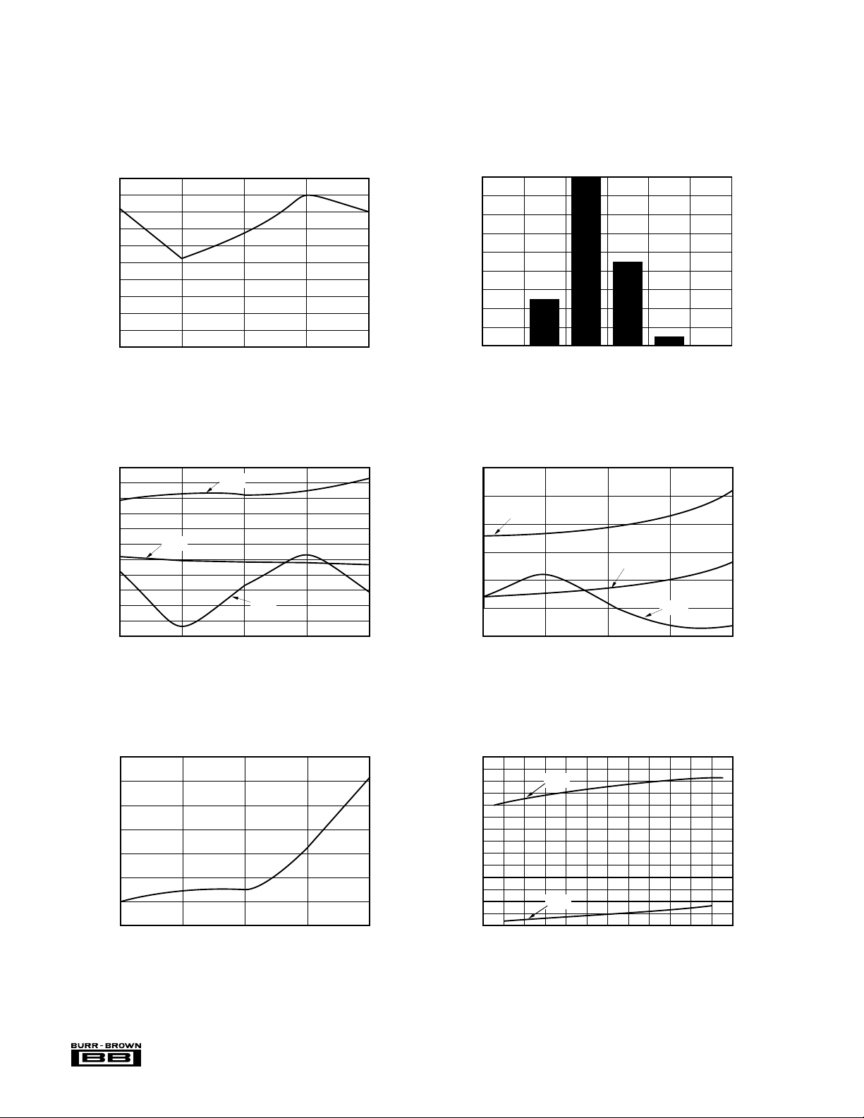
TYPICAL PERFORMANCE CURVES
At TA = +25°C, VCC = ±15V, unless otherwise noted.
10mV
9mV
8mV
7mV
6mV
5mV
4mV
BPZ Error (mV)
3mV
2mV
1mV
0
–25 0 25 70 125
BPZ ERROR vs TEMPERATURE
Temperature (°C)
BIPOLAR GAIN ERROR as % FSR
25°C; N = 33 UNITS
18
16
14
12
10
8
6
Number of Units
4
2
0
–0.35 –0.45 –0.60
–0.40 –0.55
–0.50
% FSR
0.012
0.010
–V
CC
0.008
0.006
0.004
PSRR at +FS INPUT
0.002
% / %
–0.002
0
+V
CC
–0.004
–0.006
V
DD
–0.008
–0.010
–25 0 25 70 125
Temperature (°C)
V vs TEMP
2.002
REF
2.000
1.998
1.996
REF
1.994
V (V)
1.992
1.99
1.988
–25 0 25 70 125
Temperature (°C)
0.012
PSRR at –FS INPUT
0.01
–V
0.008
0.006
% / %
CC
+V
CC
0.004
0.002
V
DD
0
–25 0 25 70 125
Temperature (°C)
I vs SUPPLY VOLTAGE
–V
SS
CC
21
20
19
18
17
Current (mA)
16
15
+V
CC
14
41016
6 8 12 14
Supply Voltage (V)
®
PCM78 4
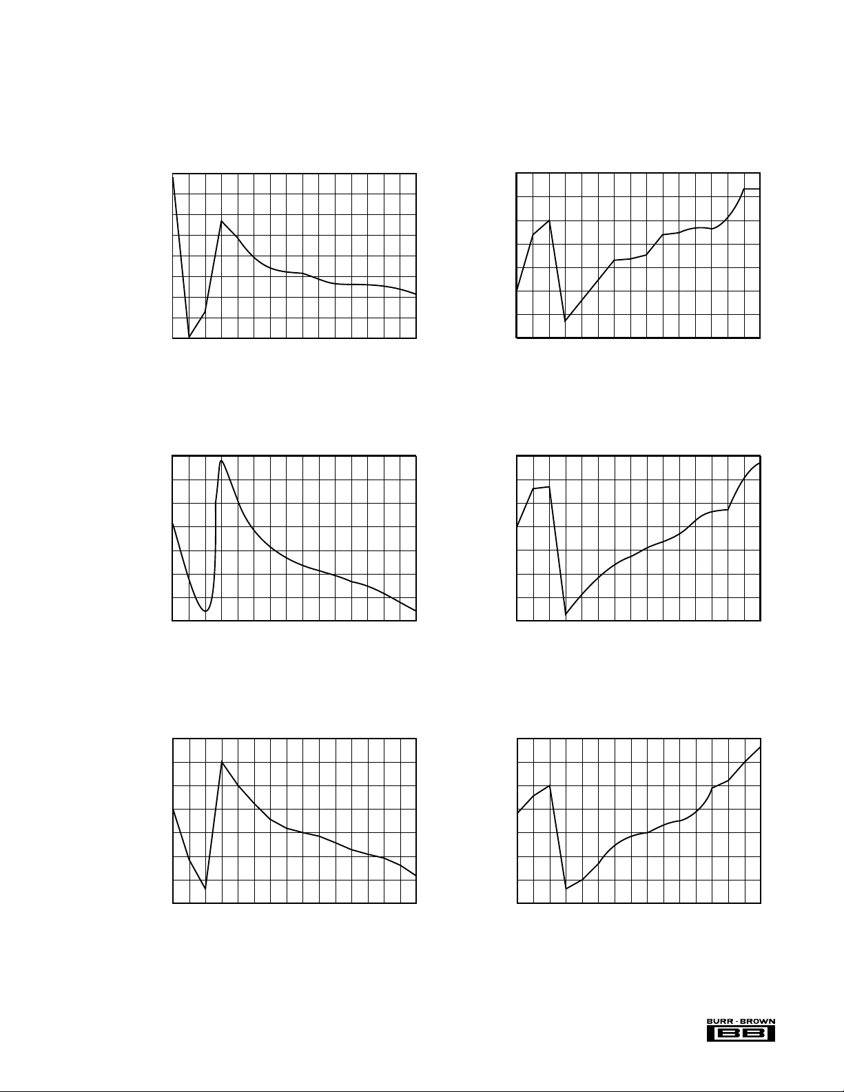
DIFFERENTIAL NONLINEARITY
at 25°C
1.40
0.80
0.60
0.00
1
1.20
LSB
0.20
Major Carry Bit Number
1.00
0.40
2345678910111213141516
DIFFERENTIAL NONLINEARITY
at 0°C
1.40
0.80
0.60
0.00
1
1.20
LSB
0.20
Major Carry Bit Number
1.00
0.40
2345678910111213141516
DIFFERENTIAL NONLINEARITY
at –25°C
1.40
1.00
0.00
1
LSB
Major Carry Bit Number
1.20
0.80
2345678910111213141516
0.60
0.40
0.20
TYPICAL PERFORMANCE CURVES (CONT)
At TA = +25°C, VCC = ±15V, unless otherwise noted.
INTEGRAL NONLINEARITY
at –25°C
Major Carry Bit Number
LSB
7.00
6.00
5.00
4.00
3.00
2.00
1.00
0.00
–1.00
2345678910111213141516
1
LSB
LSB
5.00
4.00
3.00
2.00
1.00
0.00
–1.00
–2.00
5.00
4.00
3.00
2.00
1.00
INTEGRAL NONLINEARITY
2345678910111213141516
1
INTEGRAL NONLINEARITY
at 0°C
Major Carry Bit Number
at 25°C
0.00
–1.00
–2.00
2345678910111213141516
1
Major Carry Bit Number
®
PCM785
 Loading...