

Burr Brown PCM63P, PCM63P-J, PCM63P-K Datasheet
®
PCM63P
PCM63P
DEMO BOARD
AVAILABLE
See Appendix A
Colinear
™
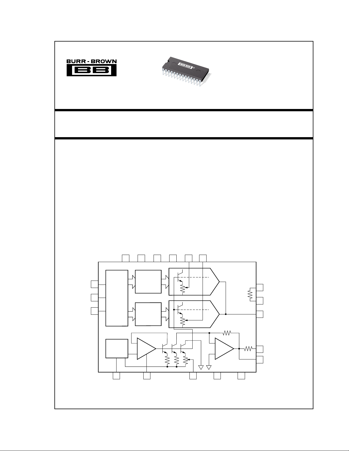
20-Bit Monolithic Audio
DIGITAL-TO-ANALOG CONVERTER
FEATURES
●
COLINEAR
● NEAR-IDEAL LOW LEVEL OPERATION
● GLITCH-FREE OUTPUT
● ULTRA LOW –96dB max THD+N
(Without External Adjustment)
● 116dB SNR min (A-Weight Method)
● INDUSTRY STD SERIAL INPUT FORMAT
● FAST (200ns) CURRENT OUTPUT
(±2mA; ±2% max)
● CAPABLE OF 16x OVERSAMPLING
● COMPLETE WITH REFERENCE
Clock
Latch Enable
Data
20-BIT AUDIO DAC
+5V
Analog
213
18
Input Shift
20
21
Register
and
Control
Logic
+5V
Analog
Digital
Upper DAC
Positive
Data Latches
Lower DAC
Negative
Data Latches
–5V
28 11
Digital
–5V
DESCRIPTION
The PCM63P is a precision 20-bit digital-to-analog
converter with ultra-low distortion (–96dB max with a
full scale output; PCM63P-K). Incorporated into the
PCM63P is a unique
architecture that eliminates unwanted glitches and
other nonlinearities around bipolar zero. The PCM63P
also features a very low noise (116dB max SNR;
A-weighted method) and fast settling current output
(200ns typ, 2mA step) which is capable of 16-times
oversampling rates.
Applications include very low distortion frequency
synthesis and high-end consumer and professional
digital audio applications.
Upper
Lower
B2 Adj
B2 Adj
23 24
19-Bit
Upper
DAC
19-Bit
Lower
DAC
PCM63P
Colinear
Colinear
20-Bit DAC
dual-DAC per channel
9
R
FEEDBACK
10
R
FEEDBACK
6
I
OUT
Buried
Zener
Reference
31
Reference
Decouple
Colinear
™, Burr-Brown Corp.
International Airport Industrial Park • Mailing Address: PO Box 11400, Tucson, AZ 85734 • Street Address: 6730 S. Tucson Blvd., Tucson, AZ 85706 • Tel: (520) 746-1111 • Twx: 910-952-1111
Internet: http://www.burr-brown.com/ • FAXLine: (800) 548-6133 (US/Canada Only) • Cable: BBRCORP • Telex: 066-6491 • FAX: (520) 889-1510 • Immediate Product Info: (800) 548-6132
© 1990 Burr-Brown Corporation PDS-1083F Printed in U.S.A. January, 1998
Servo
Amp
Servo
Decouple
Ref
Amp
25 7 12
Potentiometer
Voltage
Analog
Common
1
Digital
Common
54Bipolar Offset Current
Offset Decouple
®
PCM63P
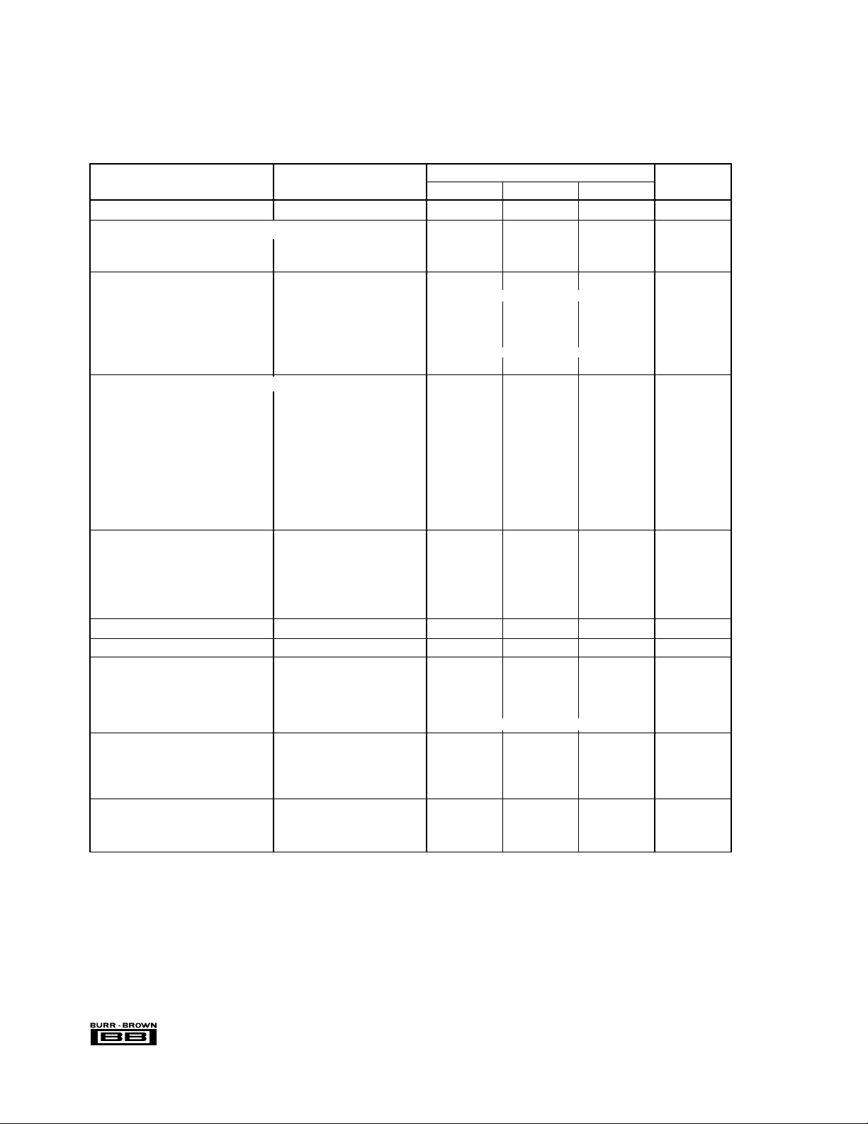
SPECIFICATIONS
ELECTRICAL
All specifications at 25°C and ±VA and ±VD = ±5V, unless otherwise noted.
PCM63P, PCM63P-J, PCM63P-K
PARAMETER CONDITIONS MIN TYP MAX UNITS
RESOLUTION 20 Bits
DYNAMIC RANGE, ΤΗD+Ν at –60dB Referred to Full Scale
PCM63P 96 100 dB
PCM63P-J 100 104 dB
PCM63P-K 104 108 dB
DIGITAL INPUT
Logic Family TTL/CMOS Compatible
Logic Level: V
Data Format Serial, MSB First, BTC
IH
V
IL
I
IH
I
IL
VIH = +2.7V +1 µA
VIL = +0.4V –50 µA
Input Clock Frequency 12.5 25 MHz
(2)
TOTAL HARMONIC DISTORTION + N
PCM63P
f = 991Hz (0dB)
(3)
f = 991Hz (–20dB) f
f = 991Hz (–60dB) f
PCM63P-J
f = 991Hz (0dB) f
f = 991Hz (–20dB) f
f = 991Hz (–60dB) f
PCM63P-K
f = 991Hz (0dB) f
f = 991Hz (–20dB) f
f = 991Hz (–60dB) f
, Without Adjustments
fS = 352.8kHz
= 352.8kHz –80 –74 dB
S
= 352.8kHz –40 –36 dB
S
= 352.8kHz –96 –92 dB
S
= 352.8kHz –82 –76 dB
S
= 352.8kHz –44 –40 dB
S
= 352.8kHz –100 –96 dB
S
= 352.8kHz –88 –82 dB
S
= 352.8kHz –48 –44 dB
S
(4)
ACCURACY
Level Linearity at –90dB Signal Level ±0.3 ±1dB
Gain Error ±1 ± 2%
Bipolar Zero Error
(5)
Gain Drift 0°C to 70°C 25 ppm/°C
Bipolar Zero Drift 0°C to 70°C 4 ppm of FSR/°C
Warm-up Time 1 Minute
IDLE CHANNEL SNR
(6)
20Hz to 20kHz at BPZ
(7)
POWER SUPPLY REJECTION +86 dB
ANALOG OUTPUT
Output Range ±2.00 mA
Output Impedance 670 Ω
Internal R
FEEDBACK
Settling Time 2mA Step 200 ns
Glitch Energy No Glitch Around Zero
POWER SUPPLY REQUIREMENTS
, ±VD Supply Voltage Range ±4.50 ± 5 ±5.50 V
±V
A
, +ID Combined Supply Current +VA, +VD = +5V 10 15 mA
+I
A
, –ID Combined Supply Current –VA, –VD = –5V –35 –45 mA
–I
A
Power Dissipation ±V
, ±VD = ±5V 225 300 mW
A
TEMPERATURE RANGE
Specification 0 +70 °C
Operating –40 +85 °C
Storage –60 +100 °C
NOTES: (1) Binary Two’s Complement coding. (2) Ratio of (Distortion
converter sample frequency (8 x 44.1kHz; 8x oversampling). (5) Offset error at bipolar zero. (6) Measured using an OPA27 and 1.5kΩ feedback and an A-weighted
RMS
+ Noise
filter. (7) Bipolar Zero.
+2.4 +V
0 0.8 V
D
(1)
–92 –88 dB
±12 µA
+116 +120 dB
1.5 kΩ
RMS
) / Signal
. (3) D/A converter output frequency (signal level). (4) D/A
RMS
V
The information provided herein is believed to be reliable; however, BURR-BROWN assumes no responsibility for inaccuracies or omissions. BURR-BROWN assumes
no responsibility for the use of this information, and all use of such information shall be entirely at the user’s own risk. Prices and specifications are subject to change
without notice. No patent rights or licenses to any of the circuits described herein are implied or granted to any third party. BURR-BROWN does not authorize or warrant
any BURR-BROWN product for use in life support devices and/or systems.
®
PCM63P
2
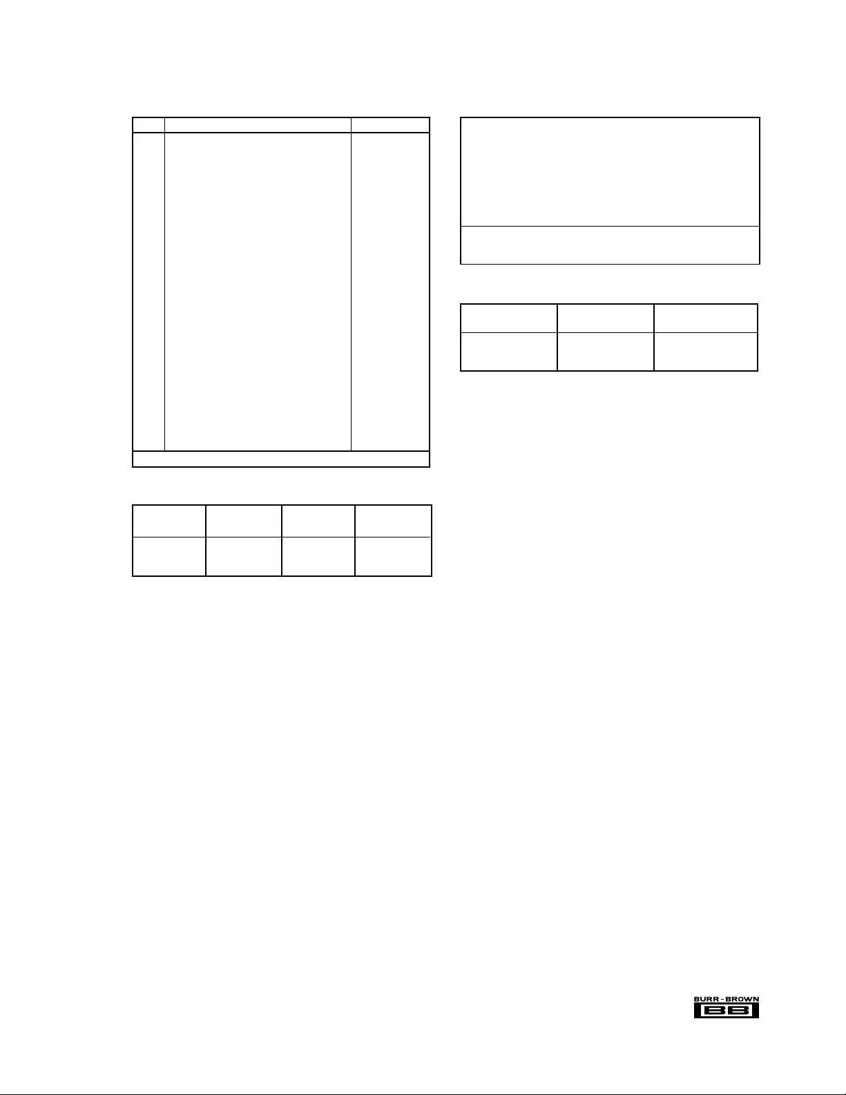
PIN ASSIGNMENTS
PIN DESCRIPTION MNEMONIC
P1 Servo Amp Decoupling Capacitor CAP
P2 +5V Analog Supply Voltage +V
P3 Reference Decoupling Capacitor CAP
A
P4 Offset Decoupling Capacitor CAP
P5 Bipolar Offset Current Output (+2mA) BPO
P6 DAC Current Output (0 to –4mA) I
P7 Analog Common Connection ACOM
OUT
P8 No Connection NC
P9 Feedback Resistor Connection (1.5kΩ)RF
P10 Feedback Resistor Connection (1.5kΩ)RF
P11 –5V Digital Supply Voltage –V
P12 Digital Common Connection DCOM
P13 +5V Digital Voltage Supply +V
P14 No Connection NC
1
2
D
D
P15 No Connection NC
P16 No Connection NC
P17 No Connection NC
P18 DAC Data Clock Input CLK
P19 No Connection NC
P20 DAC Data Latch Enable LE
P21 DAC Data Input DATA
P22 No Connection NC
P23 Optional Upper DAC Bit-2 Adjust (–4.29V)* UB2 Adj
P24 Optional Lower DAC Bit-2 Adjust (–4.29V)* LB2 Adj
P25 Bit Adjust Reference Voltage Tap (–3.52V)* V
P26 No Connection NC
POT
P27 No Connection NC
P28 –5V Analog Supply Voltage –V
A
*Nominal voltages at these nodes assuming ±VA; ±VD = ±5V.
ORDERING INFORMATION
PRODUCT PACKAGE RANGE AT 0dB
PCM63P 28-Pin Plastic DIP 0°C to +70°C –88dB
PCM63P-J 28-Pin Plastic DIP 0°C to +70°C –92dB
PCM63P-K 28-Pin Plastic DIP 0°C to +70°C –96dB
TEMPERATURE MAX THD+N,
ABSOLUTE MAXIMUM RATINGS
+VA, +VD to ACOM/DCOM........................................................0V to +8V
, –VD to ACOM/DCOM ........................................................ 0V to –8V
–V
A
, –VD to +VA, +VD............................................................. 0V to +16V
–V
A
ACOM to DCOM ............................................................................... ±0.5V
Digital Inputs (pins 18, 20, 21) to DCOM ............................... –1V to +V
Power Dissipation .......................................................................... 500mW
D
Lead Temperature, (soldering, 10s) .............................................. +300°C
Max Junction Temperature .............................................................. 165°C
θ
Thermal Resistance,
...............................................................70°C/W
JA
NOTE: Stresses above those listed under “Absolute Maximum Ratings”
may cause permanent damage to the device. Exposure to absolute
maximum conditions for extended periods may affect device reliability.
PACKAGE INFORMATION
PRODUCT PACKAGE NUMBER
PACKAGE DRAWING
PCM63P 28-Pin Plastic DIP 215
PCM63P-J 28-Pin Plastic DIP 215
PCM63P-K 28-Pin Plastic DIP 215
NOTE: (1) For detailed drawing and dimension table, please see end of data
sheet, or Appendix C of Burr-Brown IC Data Book.
(1)
®
3
PCM63P
 Loading...