

Page 1

SLAS529A – JANUARY 2007 – REVISED FEBRUARY 2007
16-Bit, Low-Power Stereo Audio CODEC With Microphone Bias, Headphone, and Digital
Speaker Amplifier
PCM3793A
PCM3794A
FEATURES
• 2 (I2C) or 3 (SPI) Wire Serial Control
• Analog Front End: • Programmable Function by Register Control:
– Stereo Single-Ended Input With Multiplexer – Digital Attenuation of DAC: 0 dB to –62 dB
– Mono Differential Input – Digital Gain of DAC: 0, 6, 12, 18 dB
– Stereo Programmable Gain Amplifier – Power Up/Down Control for Each Module
– Microphone Amplifier (20 dB) and Bias – 6-dB to –70-dB Gain for Analog Outputs
• Analog Back End: – 30-dB to –12-dB Gain for Analog Inputs
– Stereo/Mono Line Output With Volume – 0/20 dB Selectable for Microphone Input
– Stereo/Mono Headphone Amplifier With – 0-dB to –21-dB Gain for Analog Mixing
Volume and Capless Mode
– Stereo/Mono Digital Speaker Amplifier
(BTL) With Volume
• Analog Performance:
– Dynamic Range: 93 dB (DAC)
– Dynamic Range: 90 dB (ADC)
– 40-mW + 40-mW Headphone Output at
R
= 16 Ω
L
– 700-mW + 700-mW Speaker Output at
R
= 8 Ω
L
• Power Supply Voltage
– 1.71 V to 3.6 V for Digital I/O Section
– 1.71 V to 3.6 V for Digital Core Section
– 2.4 V to 3.6 V for Analog Section
– Parameter Settings for ALC
– Three-Band Tone Control and 3D Sound
– High-Pass Filter: 4-, 120-, 240-Hz
– Two-Stage Programmable Notch Filter
– Analog Mixing Control
• Pop-Noise Reduction Circuit
• Short and Thermal Protection Circuit
• Package: 5-mm × 5-mm QFN Pacakge
• Operation Temperature Range: –40 ° C to 85 ° C
APPLICATIONS
• Portable Audio Player, Cellular Phone
• Video Camcorder, Digital Movie/Still Camera
• PMP/DMB
– 2.4 V to 3.6 V for Power Amplifier Section
• Low Power Dissipation:
– 7 mW in Playback, 1.8 V/2.4 V, 48 kHz
– 13 mW in Record, 1.8 V/2.4 V, 48 kHz
– 3.3 µ W in Power Down
• Sampling Frequency: 5 kHz to 50 kHz
• Automatic Level Control for Recording
• Operation From a Single Clock Input Without
PLL
• System Clock:
– Common-Audio Clock (256 fS/384 fS), 12/24,
13/26, 13.5/27, 19.2/38.4, 19.68/39.36 MHz
• Headphone Plug Insert Detection
DESCRIPTION
The PCM3793A/94A is a low-power stereo CODEC
designed for portable digital audio applications. The
device integrates stereo digital speaker amplifier,
headphone amplifier, line amplifier, line input, boost
amplifier, microphone bias, programmable gain
control, analog mixing, sound effects, and automatic
level control (ALC). It is available in a small-footprint,
5-mm × 5-mm QFN package. The PCM3793A/94A
supports right-justified, left-justified, I2S, and DSP
formats, providing easy interfacing to audio DSP and
decoder/encoder chips. Sampling rates up to 50 kHz
are supported. The user-programmable functions are
accessible through a two- or three-wire serial control
port.
Please be aware that an important notice concerning availability, standard warranty, and use in critical applications of Texas
Instruments semiconductor products and disclaimers thereto appears at the end of this data sheet.
PRODUCTION DATA information is current as of publication date.
Products conform to specifications per the terms of the Texas
Instruments standard warranty. Production processing does not
necessarily include testing of all parameters.
Copyright © 2007, Texas Instruments Incorporated
Page 2
www.ti.com
PCM3793A
PCM3794A
SLAS529A – JANUARY 2007 – REVISED FEBRUARY 2007
This integrated circuit can be damaged by ESD. Texas Instruments recommends that all integrated circuits be handled with
appropriate precautions. Failure to observe proper handling and installation procedures can cause damage.
ESD damage can range from subtle performance degradation to complete device failure. Precision integrated circuits may be
more susceptible to damage because very small parametric changes could cause the device not to meet its published
specifications.
ABSOLUTE MAXIMUM RATINGS
over operating free-air temperature range (unless otherwise noted)
Supply voltage VDD, VIO, VCC, V
Ground voltage differences: DGND, AGND, PGND ± 0.1 V
Input voltage –0.3 to 4 V
Input current (any pins except supplies and SPK out) ±10 mA
Ambient temperature under bias –40 to 110 ° C
Storage temperature –55 to 150 ° C
Junction temperature 150 ° C
Lead temperature (soldering) 260 ° C, 5 s
Package temperature (reflow, peak) 260 ° C
(1) Stresses beyond those listed under absolute maximum ratings may cause permanent damage to the device. These are stress ratings
only, and functional operation of the device at these or any other conditions beyond those indicated under recommended operating
conditions is not implied. Exposure to absolute–maximum–rated conditions for extended periods may affect device reliability.
PA
(1)
MAX UNIT
–0.3 to 4 V
RECOMMENDED OPERATING CONDITIONS
over operating free-air temperature range (unless otherwise noted)
VCC, V
VDD, V
T
A
Analog supply voltage 2.4 3.3 3.6 V
PA
Digital supply voltage 1.71 3.3 3.6 V
IO
Digital input logic family CMOS
Digital input clock frequency
Analog output load resistance HPOL and HPOR 16 Ω
Analog output load capacitance 30 pF
Digital output load capacitance 10 pF
Operating free-air temperature –40 85 ° C
SCKI system clock 3.072 18.432 MHz
LRCK sampling clock 8 48 kHz
LOL and LOR 10 k Ω
SPOLP, SPOLN, SPORP and SPORN 8 Ω
MIN NOM MAX UNIT
2
Submit Documentation Feedback
Page 3
www.ti.com
PCM3793A
PCM3794A
SLAS529A – JANUARY 2007 – REVISED FEBRUARY 2007
ELECTRICAL CHARACTERISTICS
All specifications at TA= 25 ° C, V
otherwise noted).
PARAMETER TEST CONDITIONS UNIT
Audio Data Characteristics
DATA FORMAT
Resolution 16 Bits
Audio data interface format
Audio data bit length 16 Bits
Audio data format 2s
Sampling frequency (fS) 5 50 kHz
System clock MHz
Digital Input/Output
Logic family
V
IH
V
I
IH
I
IL
V
V
Digital Input to Line Output Through DAC (LOL, LOR, and MONO)
RL= 10 k Ω , ALC = OFF, volume = 0 dB, speaker = powered down, analog mixing = disabled
DYNAMIC PERFORMANCE
SNR Signal-to-noise ratio EIAJ, A-weighted 86 93 dB
THD+N Total harmonic distortion + noise 0 dB 0.008%
Line Input to Line Output Through Mixing Path (LOL, LOR, and MONO)
RL= 10 k Ω , ALC = OFF, volume = 0 dB, speaker = powered down, analog mixing = enabled
DYNAMIC PERFORMANCE
SNR Signal-to-noise ratio EIAJ, A-weighted 84 93 dB
Input logic level VDC
IL
Input logic current µ A
OH
Output logic level VDC
OL
Full-scale output voltage 0 dB
Dynamic range EIAJ, A-weighted 93 dB
Channel separation 91 dB
Load resistance 10 k Ω
Full-scale input and output
voltage
= V
= V
= V
DD
IO
CC
= 3.3 V, fS= 48 kHz, system clock = 256 fS, and 16-bit data (unless
PA
PCM3793ARHB, PCM3794ARHB
MIN TYP MAX
I2S, left-,
right-
justified,
DSP
MSB first,
complement
V
< 2 V 27
DD
V
> 2 V 40
DD
CMOS
compatible
0.7 V
IO
0.3 V
IO
VIN= 3.3 V 10
VIN= 0 V –10
IOH= –2 mA 0.75 V
IOL= 2 mA 0.25 V
IO
IO
2.828 Vp-p
1 Vrms
0 dB
2.828 Vp-p
1 Vrms
Submit Documentation Feedback
3
Page 4
www.ti.com
PCM3793A
PCM3794A
SLAS529A – JANUARY 2007 – REVISED FEBRUARY 2007
ELECTRICAL CHARACTERISTICS (continued)
All specifications at TA= 25 ° C, V
otherwise noted).
PARAMETER TEST CONDITIONS UNIT
Digital Input to Headphone Output Through DAC (HPOL and HPOR)
RL= 16 Ω or 32 Ω , ALC = OFF, volume = 0 dB, speaker = powered down, analog mixing = disabled, not capless mode
DYNAMIC PERFORMANCE
Full-scale output voltage 0 dB
SNR Signal-to-noise ratio EIAJ, A-weighted 84 93 dB
THD+N Total harmonic distortion + noise
Load resistance 16 Ω
PSRR Power-supply rejection ratio 1 kHz, 140 mVp-p –45 dB
Line Input to Headphone Output Through Mixing Path (HPOL and HPOR)
RL= 16 Ω or 32 Ω , ALC = OFF, volume = 0 dB, speaker = powered down, analog mixing = enabled, not capless mode
DYNAMIC PERFORMANCE
Full-scale output voltage 0 dB
SNR Signal-to-noise ratio EIAJ, A-weighted 84 93 dB
Load resistance 16 Ω
Digital Input to Speaker Output Through DAC (SPOLP, SPOLN, SPORP, and SPORN): PCM3793A
RL= 8 Ω , ALC = OFF, volume = 0 dB, headphone = powered down, analog mixing = disabled
DYNAMIC PERFORMANCE
Full-scale output voltage 0 dB
SNR Signal-to-noise ratio EIAJ, A-weighted 84 93 dB
THD+N Total harmonic distortion + noise 400 mW, RL= 8 Ω , volume = 0 dB 0.3%
Load resistance 8 Ω
PSRR Power-supply rejection ratio 1 kHz, 140 mVp-p –45 dB
Line Input to Speaker Output Through Mixing Path (SPOLP, SPOLN, SPORP, and SPORN): PCM3793A
RL= 8 Ω , ALC = OFF, volume = 0 dB, headphone = powered down, analog mixing = enabled
DYNAMIC PERFORMANCE
Full-scale output voltage 0 dB
SNR Signal-to-noise ratio EIAJ, A-Weighted 84 93 dB
= V
= V
= V
DD
IO
CC
30 mW, RL= 32 Ω , volume = 0 dB 0.1%
40 mW, RL= 16 Ω , volume = –1 dB 0.03%
200 Hz, 140 mVp-p –40
20 kHz, 140 mVp-p –32
200 Hz, 140 mVp-p –50
20 kHz, 140 mVp-p –25
= 3.3 V, fS= 48 kHz, system clock = 256 fS, and 16-bit data (unless
PA
PCM3793ARHB, PCM3794ARHB
MIN TYP MAX
2.828 Vp-p
2.828 Vp-p
2.52 Vp-p
0.9 Vrms
2.52 Vp-p
0.9 Vrms
1 Vrms
1 Vrms
4
Submit Documentation Feedback
Page 5
www.ti.com
PCM3793A
PCM3794A
SLAS529A – JANUARY 2007 – REVISED FEBRUARY 2007
ELECTRICAL CHARACTERISTICS (continued)
All specifications at TA= 25 ° C, V
otherwise noted).
PARAMETER TEST CONDITIONS UNIT
Line Input to Digital Output Through ADC (AIN1L/R, AIN2L/R, AIN3L, and AIN3L/R)
ALC = OFF, microphone boost = 0 dB, PGA = 0 dB, speaker and headphone = powered down, analog mixing = disabled
DYNAMIC PERFORMANCE
Full-scale input voltage 0 dB
Dynamic range EIAJ, A-weighted 90 dB
SNR Signal-to-noise ratio EIAJ, A-weighted 83 90 dB
Channel separation 87 dB
THD+N Total harmonic distortion + noise –1 dB 0.009%
ANALOG INPUT
Center voltage 0.5 V
Input impedance 10 20 k Ω
Microphone Bias
ALC = OFF, microphone boost = 0 dB, PGA = 0 dB, speaker and headphone = powered down, analog mixing = disabled
Bias voltage 0.75 V
Bias source current 2 mA
Output noise 6.5 µ V
Filter Characteristics
INTERPOLATION FILTER FOR DAC
Pass band 0.454 f
Stop band 0.546 f
Pass-band ripple ± 0.04 dB
Stop-band attenuation –50 dB
Group delay 19/f
De-emphasis error ± 0.1 dB
ANALOG FILTER FOR DAC
Frequency response f = 20 kHz ± 0.2 dB
DECIMATION FILTER FOR ADC
Pass band 0.408 f
Stop band 0.591 f
Pass-band ripple ± 0.02 dB
Stop-band attenuation f < 3.268 f
Group delay 17/f
HIGH-PASS FILTER FOR ADC
Frequency response Hz
= V
= V
= V
DD
IO
CC
= 3.3 V, fS= 48 kHz, system clock = 256 fS, and 16-bit data (unless
PA
PCM3793ARHB, PCM3794ARHB
MIN TYP MAX
2.828 Vp-p
1 Vrms
CC
CC
S
S
s
S
S
S
–60 dB
S
–3 dB, fc= 4 Hz 3.74
–0.5 dB, fc= 4 Hz 10.66
–0.1 dB, fc= 4 Hz 24.2
–3 dB, fc= 240 Hz 235.68
–0.5 dB, fc= 240 Hz 609.95
–0.1 dB, fc= 240 Hz 2601.2
V
V
s
s
Submit Documentation Feedback
5
Page 6
www.ti.com
PCM3793A
PCM3794A
SLAS529A – JANUARY 2007 – REVISED FEBRUARY 2007
ELECTRICAL CHARACTERISTICS (continued)
All specifications at TA= 25 ° C, V
otherwise noted).
PARAMETER TEST CONDITIONS UNIT
Power Supply and Supply Current
V
IO
V
DD
V
V
Temperature Condition
θ
JA
Voltage range VDC
CC
PA
Supply current
Power dissipation
Operation temperature –40 85 ° C
Thermal resistance 30 ° C/W
= V
DD
= V
= V
IO
CC
BPZ input, all active, no load 24.3 35 mA
All inputs are held static 1 10 µ A
BPZ input 80.2 115.5 mW
All inputs are held static 3.3 33 µ W
= 3.3 V, fS= 48 kHz, system clock = 256 fS, and 16-bit data (unless
PA
PCM3793ARHB, PCM3794ARHB
MIN TYP MAX
1.71 3.3 3.6
1.71 3.3 3.6
2.4 3.3 3.6
2.4 3.3 3.6
6
Submit Documentation Feedback
Page 7
www.ti.com
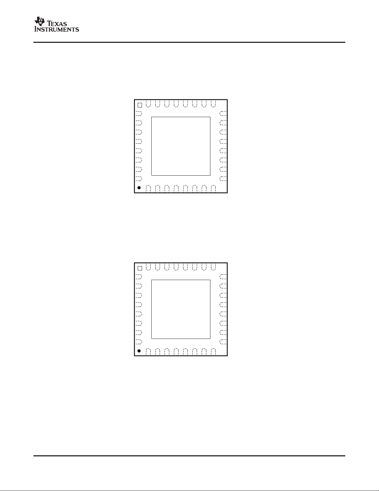
P0048-05
HPOR/LORAIN2L
BCK
AIN2R
24123222321420519618717
8
16
25
15
26
14
27
13
28
12
29
1130
1031
932
SPOLP
AIN3L
SPOLN
AIN3R
PGND
MICB
V
PA
V
CC
SPORP
AGND
SPORN
V
COM
HPCOM/MONO
HPOL/LOL
PCM3793ARHB
(TOP VIEW)
AIN1R
DIN
AIN1L
DOUT
MODE
V
IO
MS/ADR
V
DD
MD/SDA
DGND
MC/SCL
SCKI
LRCK
HDTI
P0048-06
HPOR/LORAIN2L
BCK
AIN2R
24123222321420519618717
8
16
25
15
26
14
27
13
28
12
29
1130
1031
932
NC
AIN3LNCAIN3R
PGND
MICB
V
PA
V
CC
NC
AGNDNCV
COM
HPCOM/MONO
HPOL/LOL
PCM3794ARHB
(TOP VIEW)
AIN1R
DIN
AIN1L
DOUT
MODE
V
IO
MS/ADR
V
DD
MD/SDA
DGND
MC/SCL
SCKI
LRCK
HDTI
PCM3793A
PCM3794A
SLAS529A – JANUARY 2007 – REVISED FEBRUARY 2007
PIN ASSIGNMENTS
Submit Documentation Feedback
7
Page 8
www.ti.com
PCM3793A
PCM3794A
SLAS529A – JANUARY 2007 – REVISED FEBRUARY 2007
Table 1. TERMINAL FUNCTIONS
TERMINAL
NAME PCM3793ARHB PCM3794ARHB
AGND 19 19 – Ground for analog
AIN1L 27 27 I Analog input 1 for L-channel
AIN1R 26 26 I Analog input 1 for R-channel
AIN2L 25 25 I Analog input 2 for L-channel
AIN2R 24 24 I Analog input 2 for R-channel
AIN3L 23 23 I Analog input 3 for L-channel
AIN3R 22 22 I Analog input 3 for R-channel
BCK 1 1 I/O Serial bit clock
DGND 6 6 – Digital ground
DIN 2 2 I Serial audio data input
DOUT 3 3 O Serial audio data output
HDTI 8 8 I Headphone plug insertion detection
HPCOM/MONO 9 9 O Headphone common/mono line output
HPOL/LOL 17 17 O Headphone/lineout for R-channel
HPOR/LOR 16 16 O Headphone/lineout for L-channel
LRCK 32 32 I/O Left and right channel clock
MC/SCL 31 31 I Mode control clock for three-wire/two-wire interface
MD/SDA 30 30 I/O Mode control data for three-wire/two-wire interface
MICB 21 21 O Microphone bias source output
MODE 28 28 I Two- or three-wire interface selection (LOW: SPI, HIGH: I2C)
MS/ADR 29 29 I Mode control select for three-wire/two-wire interface
PGND 13 13 – Ground for speaker power amplifier
SCKI 7 7 I System clock
SPOLN 14 – O Speaker output L-channel for negative (PCM3793A)
SPOLP 15 – O Speaker output L-channel for positive (PCM3793A)
SPORN 10 – O Speaker output R-channel for negative (PCM3793A)
SPORP 11 – O Speaker output R-channel for positive (PCM3793A)
V
CC
V
COM
V
DD
V
IO
V
PA
20 20 – Analog power supply
18 18 – Analog common voltage
5 5 – Power supply for digital core
4 4 – Power supply for digital I/O
12 12 – Power supply for power amplifier
I/O DESCRIPTION
8
Submit Documentation Feedback
Page 9
www.ti.com
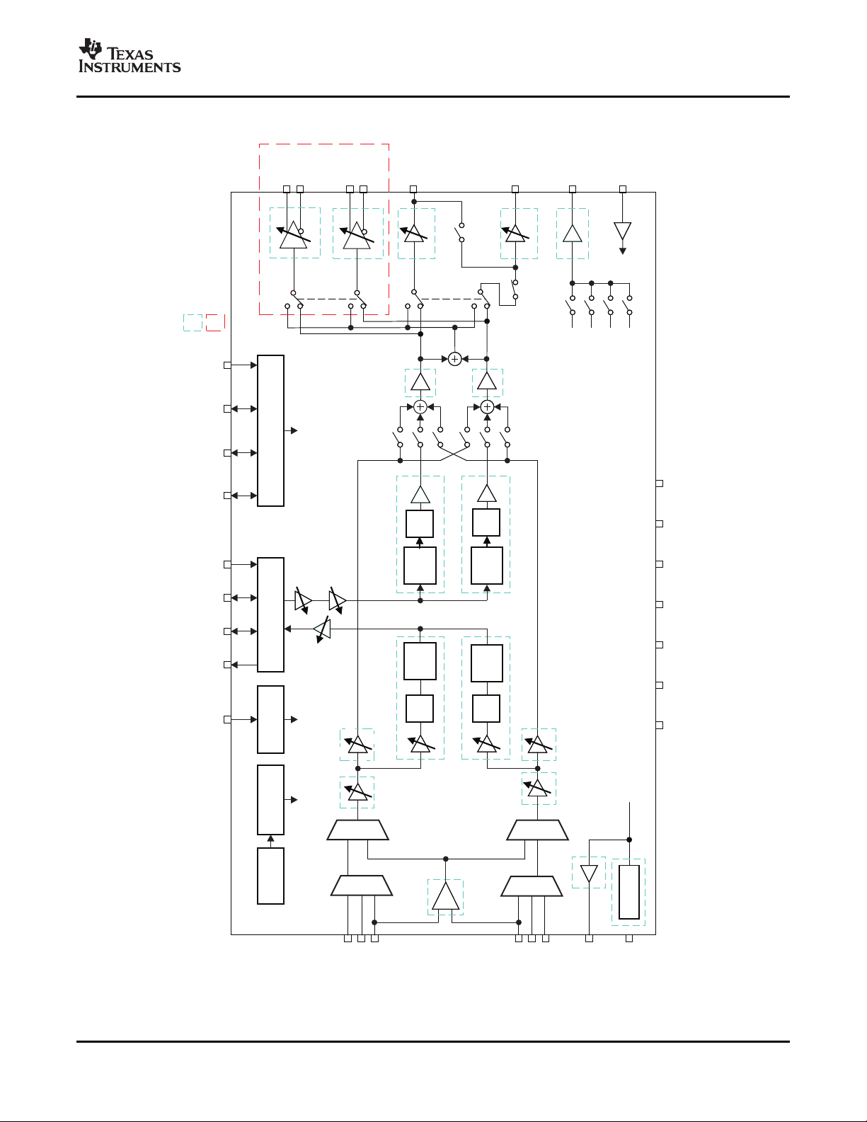
FUNCTIONAL BLOCK DIAGRAM
AIN3L
AIN2L
AIN1L
AIN1R
AIN2R
AIN3R
BCK
D
IN
DOUT
LRCK
M
S/ADRMC/SCL
M
D/SDA
MODE
Se
rial Interface (SPI/I C)
2
SCKI
Audio Interface
PGND
AGND
DGND
V
COM
MICB
SPOLP
SPOLN
SPORP
SPORN
HDTI
B
0181-02
+
6to –70dB
+6to –70dB
+6to –70dB
+6to –70dB
HP
L
SPL
SPR
MUX1
DAL
ADL
DAR
COM
HPR
HP
C
LO
UT
ROUT
PG
5
V
IO
V
D
D
V
PA
V
C
C
MON
O
M
CB
Mic Bias
C
OM
PG
1
PG
3
PG4
0/+
20dB
0/+
20dB
0to –21dB
0to –21dB
+30to –12dB
+3
0to –12dB
MONO
C
lock
M
anager
Po
wer On
Re
set
Power Up/Down
Manager
ADR
D2S
MUX3
MUX2
MUX4
PG6
PG2
Anal
og Input L-ch
Analog Input R-ch
MXL
MX
R
HP
OR
HPOL
C
OM
V
C
OM
P
ossible for Power Up/Down
P
CM3794 has no Speaker Output
S
W1
SW2
SW
3
SW6
SW5
SW4
HPOL/
LOL
HPOR/
LOR
HPCOM
/MONO
DS
ADC
DS
ADC
DS
DAC
DS
DAC
Digital
Filter
(1)
Digital
Filter
(1)
Digital
Filter
(1)
Digital
Filter
(1)
ATR
Mute
DGC
0,+6,+12,+18dB
A
TP
0to –62dB,Mute
(1)
DecimationFilter
InterpolationFilter
3-DEnhancement
3-Band
T
oneControl
NotchFilter
PCM3793A
PCM3794A
SLAS529A – JANUARY 2007 – REVISED FEBRUARY 2007
Submit Documentation Feedback
9
Page 10
www.ti.com
–120
–100
–80
–60
–40
–20
0
0 1 2 3 4
Frequency [ f ]´
S
Amplitude – dB
G001
Frequency [ f ]´
S
Amplitude – dB
–0.2
–0.1
0
0.1
0.2
0 0.1 0.2 0.3 0.4 0.5
G002
Frequency [ f ]´
S
Amplitude – dB
G003
–120
–100
–80
–60
–40
–20
0
0 1 2 3 4
Frequency [ f ]´
S
Amplitude – dB
–0.2
–0.1
0
0.1
0.2
0 0.1 0.2 0.3 0.4 0.5
G004
PCM3793A
PCM3794A
SLAS529A – JANUARY 2007 – REVISED FEBRUARY 2007
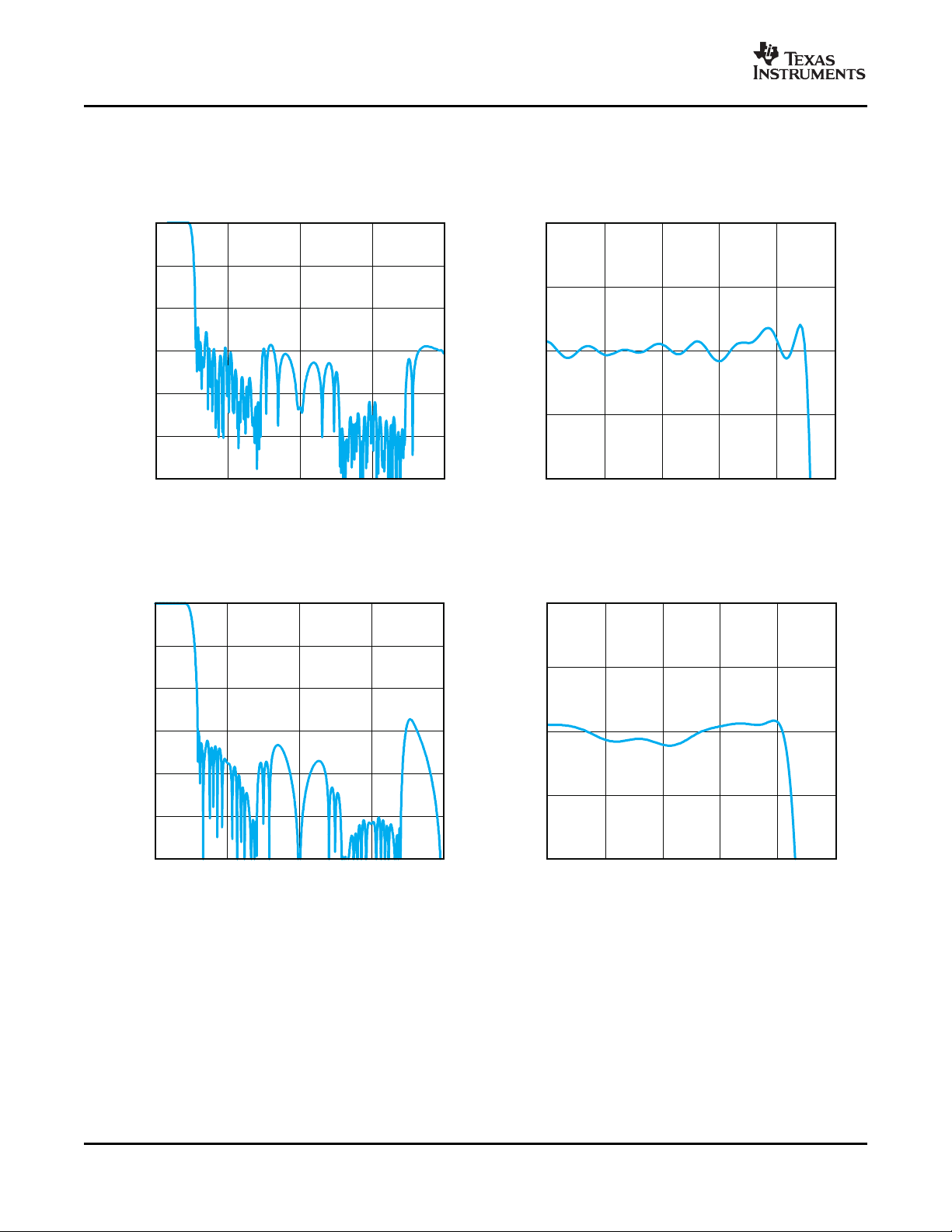
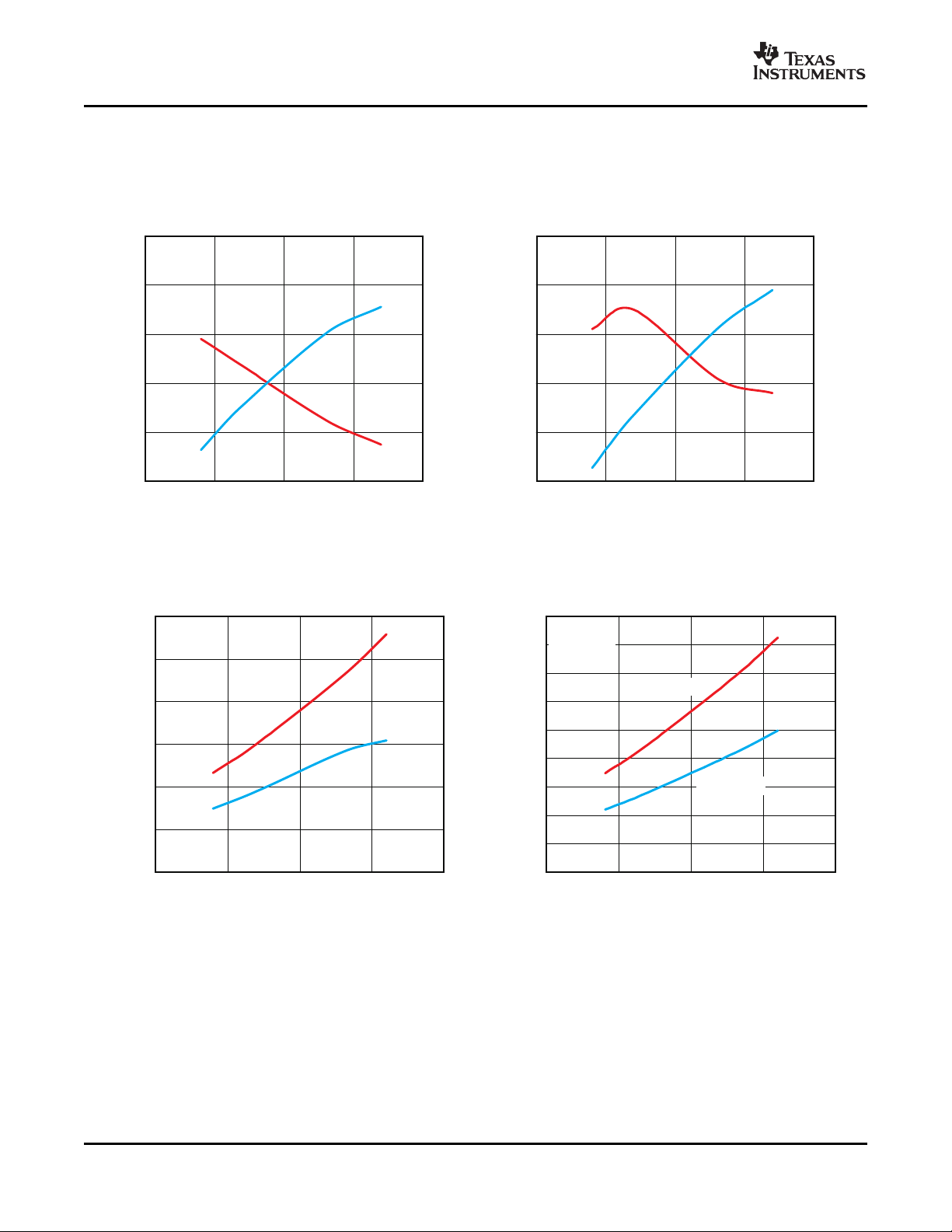
All specifications at TA= 25 ° C, V
INTERPOLATION FILTER, STOP BAND INTERPOLATION FILTER, PASS BAND
DD
TYPICAL PERFORMANCE CURVES
= V
= V
= V
IO
CC
= 3.3 V, fS= 8 to 48 kHz, system clock = 256 fS, and 16-bit data,
PA
unless otherwise noted.
Figure 1. Figure 2.
DECIMATION FILTER, STOP BAND DECIMATION FILTER, PASS BAND
Figure 3. Figure 4.
10
Submit Documentation Feedback
Page 11
www.ti.com
Frequency [ f ]´
S
Amplitude – dB
G005
–20
–15
–10
–5
0
5
0 0.0005 0.001 0.0015 0.002
Frequency [ f ]´
S
Amplitude – dB
G025
–20
–15
–10
–5
0
5
0 0.005 0.01 0.015 0.02
Frequency [ f ]´
S
Amplitude – dB
G006
–20
–15
–10
–5
0
5
0 0.01 0.02 0.03 0.04
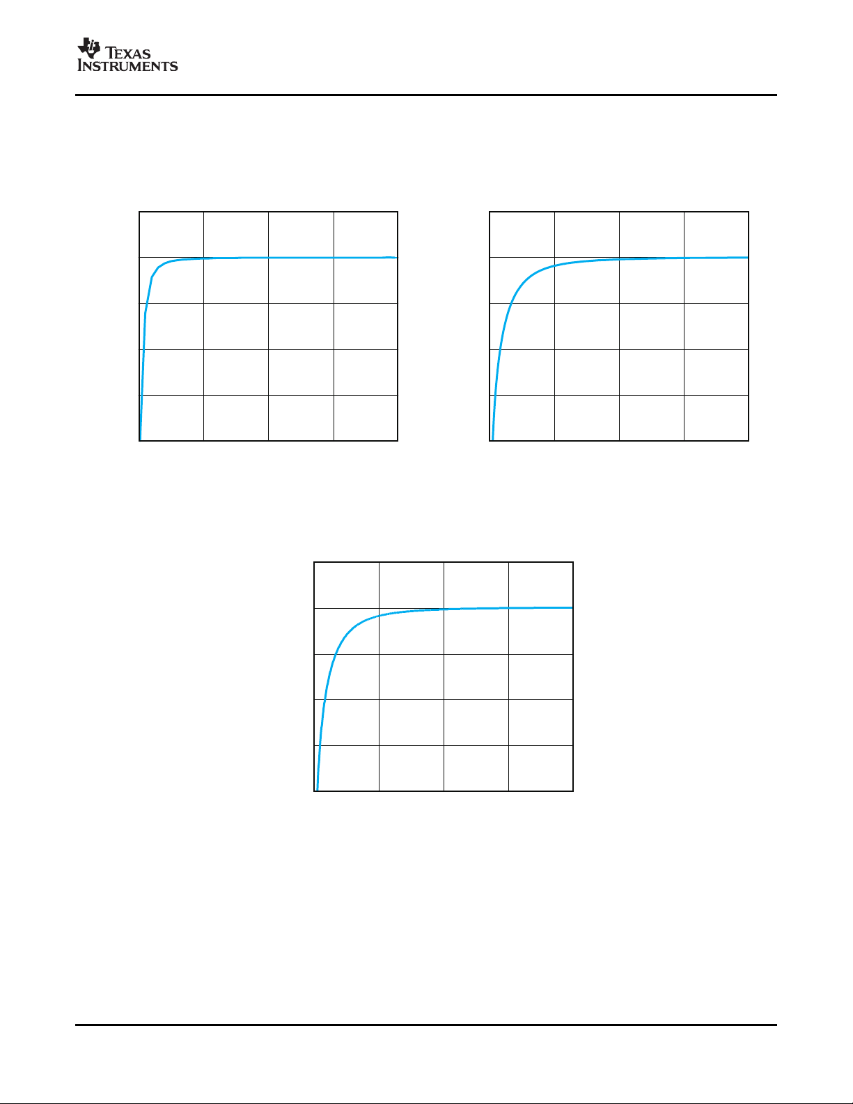
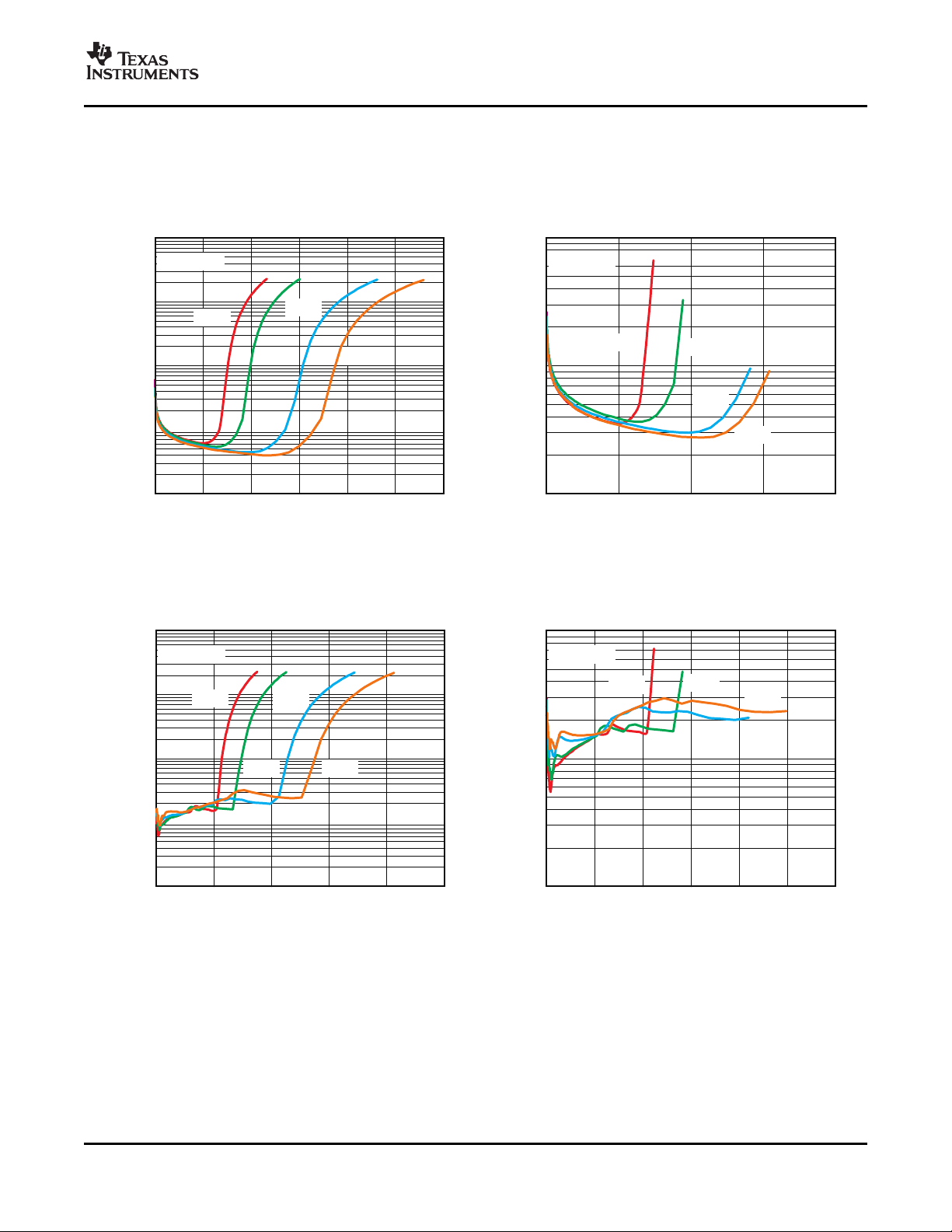
All specifications at TA= 25 ° C, V
unless otherwise noted.
TYPICAL PERFORMANCE CURVES (continued)
= V
= V
= V
DD
IO
CC
= 3.3 V, fS= 8 to 48 kHz, system clock = 256 fS, and 16-bit data,
PA
PCM3793A
PCM3794A
SLAS529A – JANUARY 2007 – REVISED FEBRUARY 2007
HIGH-PASS FILTER PASS-BAND CHARACTERISTICS HIGH-PASS FILTER PASS-BAND CHARACTERISTICS
(fC= 4 Hz at fS= 48 kHz) (fC= 120 Hz at fS= 48 kHz)
Figure 5. Figure 6.
HIGH-PASS FILTER PASS-BAND CHARACTERISTICS
(fC= 240 Hz at fS= 48 kHz)
Submit Documentation Feedback
Figure 7.
11
Page 12
www.ti.com
Frequency – Hz
Amplitude – dB
G007
–15
–10
–5
0
5
10
15
0.01 0.1 1 10 1k100 10k
100k
Frequency – Hz
Amplitude – dB
G008
–15
–10
–5
0
5
10
15
0
200
600400 800
1k
Frequency – Hz
A
mplitude – dB
G009
–15
–10
–5
0
5
10
15
0
1k
3k2k 4k
5k
Frequency – Hz
Amplitude – dB
G010
–15
–10
–5
0
5
10
15
2k
4k
8k6k 10k
12k 14k
PCM3793A
PCM3794A
SLAS529A – JANUARY 2007 – REVISED FEBRUARY 2007
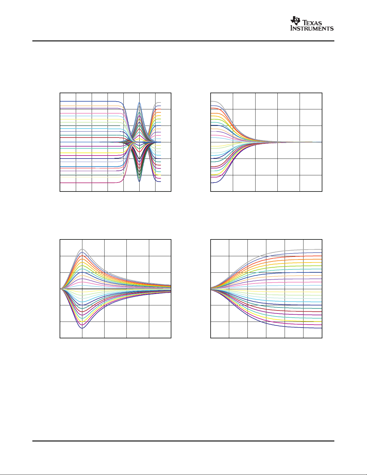
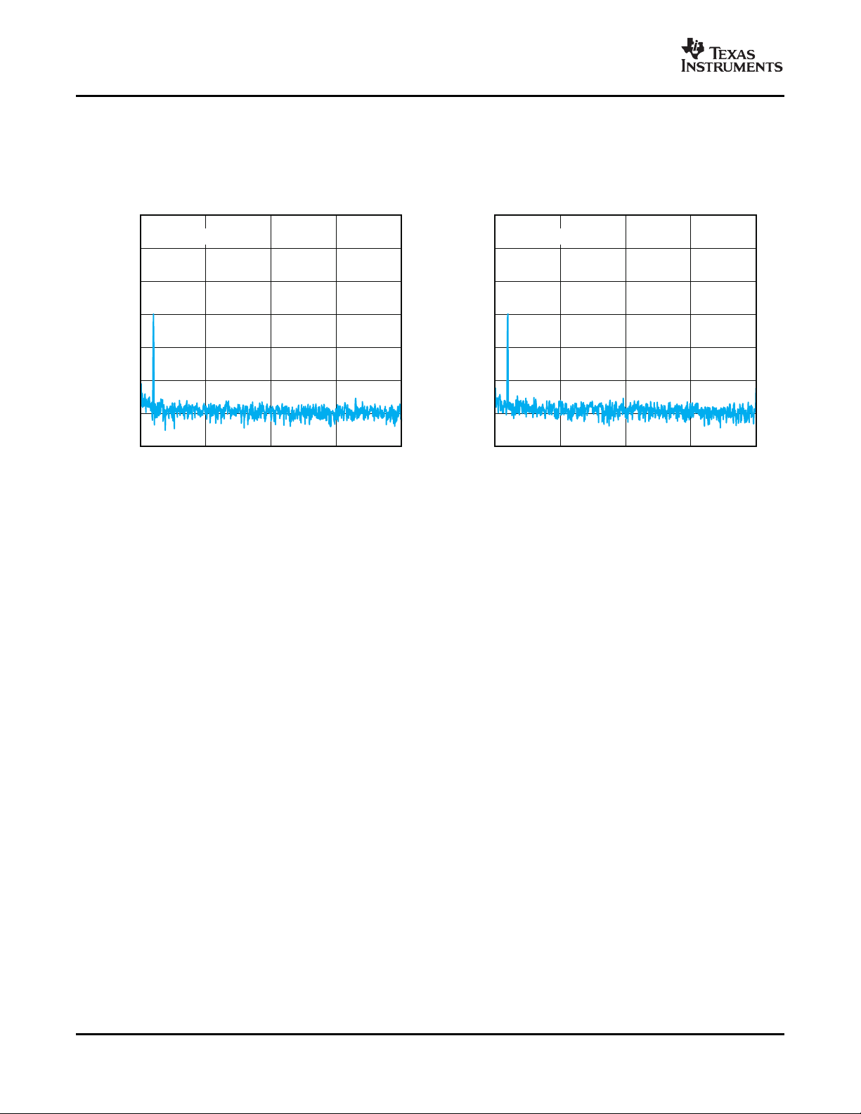
TYPICAL PERFORMANCE CURVES (continued)
All specifications at TA= 25 ° C, V
DD
= V
= V
= V
IO
CC
= 3.3 V, fS= 44.1 kHz, system clock = 256 fS, and 16-bit data, unless
PA
otherwise noted.
THREE-BAND TONE CONTROL (BASS, MIDRANGE,
TREBLE) THREE-BAND TONE CONTROL (BASS)
Figure 8. Figure 9.
THREE-BAND TONE CONTROL (MIDRANGE) THREE-BAND TONE CONTROL (TREBLE)
12
Figure 10. Figure 11.
Submit Documentation Feedback
Page 13
www.ti.com
PG3/PG4 Gain – dB
SNR – dB
G011
40
50
60
70
85
90
100
0
5
1510 20
25 30
Single Input
Differential Input
f = 1 kHz
IN
PG3/PG4 Gain – dB
SNR – dB
G012
40
45
65
60
55
50
70
75
80
85
90
0
5
1510 20
25 30
Single Input
Differential Input
f = 1 kHz
IN
Power Supply – V
THD+N – %
SNR – dB
G013
0
0.2
0.4
0.6
0.8
1
90
91
92
93
94
95
2 2.5 3.53 4
f = 1 kHz
IN
THD+N
SNR
Power Supply – V
THD+N – %
SNR – dB
G014
0
0.01
0.02
0.03
0.04
0.05
90
91
92
93
94
95
2 2.5 3.53 4
f = 1 kHz
IN
THD+N
SNR
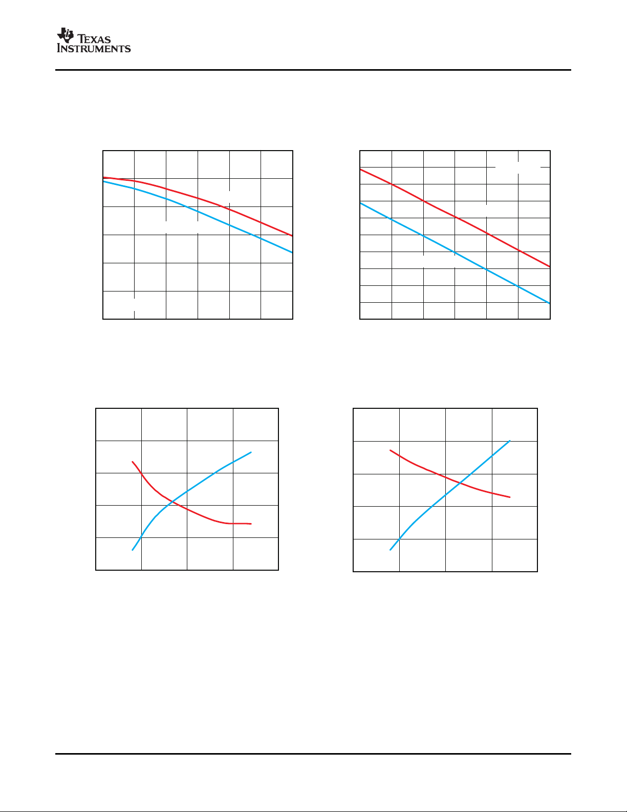
All specifications at TA= 25 ° C, V
ADC SNR AT HIGH GAIN (PG1/PG2 = 0 dB) ADC SNR AT HIGH GAIN (PG1/PG2 = 20 dB)
TYPICAL PERFORMANCE CURVES (continued)
= V
= V
= V
DD
IO
CC
= 3.3 V, fS= 48 kHz, system clock = 256 fS, and 16-bit data, unless
PA
otherwise noted.
PCM3793A
PCM3794A
SLAS529A – JANUARY 2007 – REVISED FEBRUARY 2007
THD+N/SNR vs POWER SUPPLY THD+N/SNR vs POWER SUPPLY
DAC TO SPEAKER OUTPUT, 8- Ω DAC TO HEADPHONE OUTPUT, 16- Ω
Figure 12. Figure 13.
Figure 14. Figure 15.
Submit Documentation Feedback
13
Page 14
www.ti.com
Power Supply – V
THD+N – %
SNR – dB
G015
0.007
0.008
0.009
0.010
0.011
0.012
90
91
92
93
94
95
2 2.5 3.53 4
f = 1 kHz
IN
THD+N
SNR
Power Supply – V
THD+N – %
SNR – dB
G016
0.007
0.008
0.009
0.010
0.011
0.012
87
88
89
90
91
92
2 2.5 3.53 4
f = 1 kHz
IN
THD+N
SNR
0
20
2 2.5 3.5 43
40
60
80
100
120
Power Supply – V
O
utput Power – mW
G017
Vol = 6 dB
Vol = 0 dB
f = 1 kHz
IN
Power Supply – V
Ou
tput Power – mW
G018
0
400
300
200
100
500
600
700
800
900
2
2.5 3
3.5 4
Vol = +6 dB
Vol = 0 dB
f = 1 kHz
IN
PCM3793A
PCM3794A
SLAS529A – JANUARY 2007 – REVISED FEBRUARY 2007
TYPICAL PERFORMANCE CURVES (continued)
All specifications at TA= 25 ° C, V
otherwise noted.
THD+N/SNR vs POWER SUPPLY THD+N/SNR vs POWER SUPPLY
DAC TO LINE OUTPUT, 10-k Ω ADC TO DIGITAL OUTPUT
= V
DD
= V
= V
IO
CC
= 3.3 V, fS= 48 kHz, system clock = 256 fS, and 16-bit data, unless
PA
OUTPUT POWER vs POWER SUPPLY OUTPUT POWER vs POWER SUPPLY
(HEADPHONE, 16- Ω ) (SPEAKER, 8- Ω )
14
Figure 16. Figure 17.
Figure 18. Figure 19.
Submit Documentation Feedback
Page 15
www.ti.com
Output Power – mW
T
HD+N – %
G019
0.01
0.1
1
10
100
0
20
6040 80
100 120
f = 1 kHz
IN
2.4 V
2.7 V
3.3 V
3.6 V
Output Power – mW
T
HD+N – %
G020
0.01
0.1
1
0
20
6040
80
f = 1 kHz
IN
2.4 V
2.7 V
3.3 V
3.6 V
Output Power – mW
THD+N – %
G021
0.01
0.1
1
10
100
0
200
600400 800
1000
f = 1 kHz
IN
2.4 V
2.7 V
3.3 V
3.6 V
Output Power – mW
THD+N – %
G022
0.01
0.1
1
0
100 200 300
500400
600
2.4 V
2.7 V
3.3 V
3.6 V
f = 1 kHz
IN
All specifications at TA= 25 ° C, V
otherwise noted.
THD+N vs OUTPUT POWER THD+N vs OUTPUT POWER
(HEADPHONE, 16- Ω , VOLUME = 6 dB) (HEADPHONE, 16- Ω , VOLUME = 0 dB)
TYPICAL PERFORMANCE CURVES (continued)
= V
= V
= V
DD
IO
CC
= 3.3 V, fS= 48 kHz, system clock = 256 fS, and 16-bit data, unless
PA
PCM3793A
PCM3794A
SLAS529A – JANUARY 2007 – REVISED FEBRUARY 2007
Figure 20. Figure 21.
THD+N vs OUTPUT POWER THD+N vs OUTPUT POWER
(SPEAKER, 8- Ω , VOLUME = 6 dB) (SPEAKER, 8- Ω , VOLUME = 0 dB)
Figure 22. Figure 23.
Submit Documentation Feedback
15
Page 16
www.ti.com
Frequency – kHz
Amplitude – dB
G023
–140
0 20
155 10
–120
–100
–80
–60
–40
–20
0
f = 1 kHz/–60 dB
IN
Frequency – kHz
A
mplitude – dB
G024
–140
0 20
155 10
–120
–100
–80
–60
–40
–20
0
f = 1 kHz/–60 dB
IN
PCM3793A
PCM3794A
SLAS529A – JANUARY 2007 – REVISED FEBRUARY 2007
TYPICAL PERFORMANCE CURVES (continued)
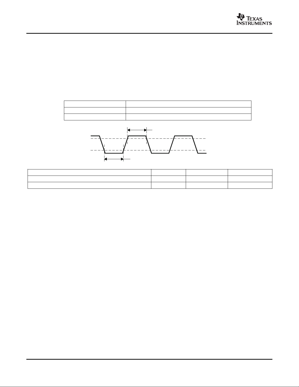
All specifications at TA= 25 ° C, V
otherwise noted.
= V
DD
= V
= V
IO
CC
= 3.3 V, fS= 48 kHz, system clock = 256 fS, and 16-bit data, unless
PA
OUTPUT SPECTRUM (DAC TO HEADPHONE OUTPUT,
16- Ω ) OUTPUT SPECTRUM (DAC TO SPEAKER OUTPUT, 8- Ω )
Figure 24. Figure 25.
16
Submit Documentation Feedback
Page 17

www.ti.com
PCM3793A
PCM3794A
SLAS529A – JANUARY 2007 – REVISED FEBRUARY 2007
PCM3793A/94A DESCRIPTION
Analog Input
The AIN1L, AIN1R, AIN2L, AIN2R, AIN3L, and AIN3R pins can be used as microphone or line inputs with
selectable 0- or 20-dB boost and 1-Vrms input. All of these analog inputs have high input impedance (20 k Ω ),
which is not changed by gain settings. One pair of inputs is selected by register 87 (AIL[1:0], AIR[1:0]). AIN1L
and AIN1R can be used as a monaural differential input.
Gain Settings for Analog Input
The gain of the analog signals can be adjusted from 30 dB to –12 dB in 1-dB steps following the 0- or 20-dB
boost amplifier. The gain level can be set for each channel by registers 79 and 80 (ALV[5:0], ARV[5:0]).
A/D Converter
The ADC includes a multilevel delta-sigma modulator, aliasing filter, decimation filter, high-pass filter, and notch
filter and can accept a 1-Vrms full-scale voltage input. The decimation filter has a digital soft mute controlled by
register 81 (RMUL, RMUR). The high-pass filter can be disabled by register 81 (HPF[1:0]), and the notch filter
can be disabled by registers 96 to 104 if it is not necessary to cancel a dc offset or compensate for wind noise.
D/A Converter
The DAC includes a multilevel delta-sigma modulator and an interpolation filter. These can be used to obtain
high PSRR, low jitter sensitivity, and low out-of-band noise quickly and easily. The interpolation filter includes
digital attenuator, digital soft mute, three-band tone control (bass, midrange and treble), and 3-D sound
controlled by registers 92 to 95. The de-emphasis filter (32, 44.1 and 48 kHz) is controlled by registers 68 to 70
(ATL[5:0], ATR[5:0], PMUL, PMUR, DEM[1:0]). Oversampling rate control can reduce out-of-band noise when
operating at low sampling rates by using register 70 (OVER).
Common Voltage
The V
pin is normally biased to 0.5 V
COM
, and it provides the common voltage to internal circuitry. It is
CC
recommended that a 4.7- µ F capacitor be connected between this pin and AGND to provide clean voltage and
avoid pop noise. The PCM3793A/94A may have a little pop noise on each analog output if a capacitor smaller
than 4.7 µ F is used.
Line Output
The HPOL/LOL, HPOR/LOR, and HPCOM/MONO pins can drive a 10-k Ω load and be configured by register 74
(HPS[1:0]) as a monaural single-ended, monaural differential, or stereo single-line output with 1-V
output.
rms
These outputs, except for the HPCOM/MONO pin, include an analog volume amplifier that can be set from 6 dB
to –70 dB and mute in steps of 0.5-, 1-, 2- or 4-dB. Each output is controlled by registers 64 and 65 (HLV[5:0],
HRV[5:0], HMUL, HMUR). No dc blocking capacitor is required when connecting an external speaker amplifier
with monaural differential input. The center voltage is 0.5 V
with zero data input.
CC
Headphone Output
The HPOL/LOL, HPOR/LOR, and HPCOM/MONO pins can be configured as a stereo, monaural, or monaural
differential headphone output by register 74 (HPS[1:0]). These pins have more than 30 or 40 mWrms output
power into a 32- or 16- Ω load, either through a dc blocking capacitor or without a capacitor. These outputs,
except for the HPCOM/MONO pin, include an analog volume amplifier that can be set from 6 dB to –70 dB in
steps of 0.5, 1, 2, or 4 dB. Each is controlled by registers 64 and 65 (HLV[5:0], HRV[5:0], HMUL, HMUR). The
center voltage is 0.5 V
with zero data input.
CC
Headphone Plug Insertion Detection
The HDTI pin detects the insertion status of headphone plug and writes the status to register 77 (HPDS), which
can be read by the I2C interface. The polarity of the status indication can be inverted by register 75 (HPDP). The
headphone and speaker amplifiers are disabled or enabled automatically by headphone plug
insertion/extractrion if register 75, HPDE = 1. They follow the register settings if register 75, HPDE = 0.
HPCOM/MONO is not affected by the status when register 74, CMS[0] = 1.
Submit Documentation Feedback
17
Page 18

www.ti.com
PCM3793A
PCM3794A
SLAS529A – JANUARY 2007 – REVISED FEBRUARY 2007
Speaker Output (Class-D, PCM3793A)
The SPOLP/SPOLN and SPORP/SPORN pins are stereo or mono speaker differential outputs (BTL) pairs with a
maximum of 700 mWrms (V
maximum battery life, minimum heat, and elimination of LC low-pass filtering. The speaker amplifier includes an
analog volume control with 6 dB to –70 dB in steps of 0.5, 1, 2 or 4 dB steps for each output, which can be set
by registers 66 (SLV[5:0] and 67 SRV[5:0]). Spectrum spreading technology and selectable switching frequency
to reduce EMI noise are controlled by register 71 (DFQ[2:0], SPS[1:0] and SPSE). This digital amplifier has a
thermal shutdown circuit that detects when the device temperature reaches approximately 150 ° C; then the
speaker amplifier is shut down.
Analog Mixing and Bypass
Mixing amplifiers (MXL, MXR) mix inputs from the AIN pins. The analog inputs are selected by register 87
(AD2S, AIR[1:0],AIL[1:0]) and can bypass the ADC/DAC and connect the mixed signal to the headphone or
speaker outputs by register 88 (MXR[2:0], MXL[2:0]). The gain of the analog inputs is controlled by register 89
(GMR[2:0], GML[2:0]). These functions are suitable for FM radio, headset, and other analog sources without an
ADC.
Microphone Bias
The MICB pin is the microphone bias source for an external microphone. MICB can provide 2 mA (typical) of
bias current.
= 3.6 V, volume = 6 dB) into an 8- Ω load. The digital speaker amplifier offers
PA
Digital Gain Control
A portable application with small speakers may be require a high sound level when playing back audio data
recorded at low level. Digital gain control (DGC) can be used to amplify the digital input data by 0, 6, 12 or 18 dB
by setting register 70 (SPX[1:0]).
Automatic Level Control (ALC) for Recording
The sound for microphone recording should be expanded to a suitable level without saturation. The digitally
controlled automatic level control (ALC) provides automatic expansion for small input signals and compression
for large input signals while recording. The expansion level, compression level, attack time, and recovery time
can be selected by register 83. The register 83 description explains the details of these settings.
3-D Sound
A 3-D sound effect is provided by mixing L-channel and R-channel data with a band-pass filter with two
parameters, mixing ratio and band pass filter characteristic, that can be controlled by register 95 (3DP[3:0],
3FLO). The 3-D sound effect uses the DAC digital input or ADC digital output selected by register 95 (SDAS).
Three-Band Tone Control
Tone control has bass, midrange, and treble controls that can be adjusted from 12 dB to –12 dB in 1-dB steps
by registers 92 to 94 (LGA[4:0], MGA[4:0] and HGA[4:0]). Register 92 (LPAE) attenuates the digital input signal
automatically to prevent clipping of the output signal at settings above 0 dB for bass control. LPAE has no effect
on midrange and treble controls.
High-Pass Filter and Two-Stage Programmable Notch Filter
The high-pass filter eliminates the dc offset of the ADC analog signal and can be set for a cutoff frequency of 4
Hz, 120 Hz, or 240 Hz at the 48-kHz sampling frequency by register 81 (HPF[1:0]). A register 95 (SDAS)
selection applies the filter to either the DAC digital input or the ADC digital output.
Notch filters are provided to remove noise of a particular frequency, such as CCD noise, motor noise, or other
mechanical noise in a particualr application. The PCM3793A/94A has two notch filters for which the center
frequency and frequency bandwidth can be programmed by registers 96 to 104. A register 95 (SDAS) selection
applies the filter to either the DAC digital input or the ADC digital output.
18
Submit Documentation Feedback
Page 19

www.ti.com
PCM3793A
PCM3794A
SLAS529A – JANUARY 2007 – REVISED FEBRUARY 2007
Digital Monaural Mixing
The audio data can be converted from stereo digital data to mixed monaural digital data. The conversion occurs
in the internal audio interface section and is controlled by register 96 (MXEN).
Zero-Cross Detection
Zero-cross detection minimizes audible zipper noise while changing analog volume and digital attenuation. This
function applies to the digital input or digital output as defined by register 86 (ZCRS).
Short Protection
The short-circuit protection on each headphone output prevents damage to the device while an output is shorted
to V
, an output is shorted to PGND, or any two outputs are shorted together. When the short circuit is detected
PA
on the outputs, the PCM3793A/94A powers down the shorted amplifier immediately. The short-protection status
can be monitored by reading register 77 (STHC, STHL, SCHR) through the I2C interface. Short-circuit protection
operates in any enabled headphone amplifier.
Thermal Protection
The thermal protection on the speaker amplifier prevents damage to the device when the internal die
temperature exceeds approximately 150 ° C. Once the die temperature exceeds the thermal set point, all analog
outputs are powered down. This status can be reset by setting register 76 (RLSR, RLSL) and can be watched
by reading register 77 (STSR, STSL) through the two-wire (I2C) interface. Thermal protection operates in any
enabled speaker amplifier.
Pop-Noise Reduction Circuit
The pop-noise reduction circuit prevents audible noise when turning the power supply on/off and powering the
device up/down in portable applications. It is recommended to establish the register settings in the sequence
that is shown in Table 3 and Table 4 . No particular external parts are required.
Power Up/Down for Each Module
Using register 72 (PMXL, PMXR), register 73 (PBIS, PDAR, PDAL, PHPC, PHPR, PHPL, PSPR, PSPL), register
82 (PAIR, PAIL, PADS, PMCB, PADR, PADL), and register 90 (PCOM), unused modules can be powered down
to minimize power consumption (7 mW during playback only and 13 mW when recording only).
Digital Audio Interface
The PCM3793A/94A can receive I2S, right-justified, left-justified, and DSP formats in both master and slave
modes. These options can be selected in register 70 (PFM[1:0]), register 81 (RFM[1:0]) and register 84 (MSTR).
Digital Interface
All digital I/O pins can interface at various power supply voltages. V
pin can be connected to a 1.71-V to 3.6-V
IO
power supply.
Power Supply
The V
The V
these pins (for example, V
pin and the V
CC
pin and the V
DD
pin can be connected to 2.4 V to 3.6 V. The same voltage must be applied to both pins.
PA
pin can be connected to 1.71 V to 3.6 V. A different voltage can be applied to each of
IO
DD
= 1.8 V, V
= 3.3 V).
IO
Submit Documentation Feedback
19
Page 20
www.ti.com
t
w(SCKH)
SCKI
t
w(SCKL)
0.7V
IO
0.3V
IO
T0005-12
PCM3793A
PCM3794A
SLAS529A – JANUARY 2007 – REVISED FEBRUARY 2007
DESCRIPTION OF OPERATION
System Clock Input
The PCM3793A/94A can accept clocks of various frequencies without a PLL. They are used for clocking the
digital filters and automatic level control and delta-sigma modulators and are classified as common-audio and
application-specific clocks. Table 2 shows frequencies of the common-audio clock and application-specific clock.
Figure 26 shows the timing requirements for system clock inputs. The sampling rate and frequency of the
system clocks are determined by the settings of register 86 (MSR[2:0]) and register 85 (NPR[5:0]). Note that the
sampling rate of the application-specific clock has a little sampling error. The details are shown in Table 12 .
Table 2. System Clock Frequencies
CLOCK FREQUENCIES
Common-audio clock 11.2896, 12.288, 16.9344, 18.432 MHz
Application-specific clock 12, 13, 13.5, 24, 26, 27, 19.2, 19.68, 38.4, 39.36 MHz
PARAMETERS SYMBOL MIN UNITS
System-clock pulse duration, high t
System-clock pulse duration, low t
w(SCKH)
w(SCKL)
7 ns
7 ns
Figure 26. System Clock Timing
Power-On Reset and System Reset
The power-on-reset circuit outputs a reset signal, typically at V
the voltage of other power supplies (V
, V
PA
, and V
CC
). Internal circuits are cleared to default status, then
IO
= 1.2 V, and this circuit does not depend on
DD
signals are removed from all analog and digital outputs. The PCM3793A/94A does not require any power supply
sequencing. Register data must be written after turning all power supplies on.
System reset is enabled by setting register 85 (SRST = 1). After the reset sequence, the register data is reset to
SRST = 0 automatically. All circuits are cleared to their default status at once by the system reset. Note that the
PCM3793A/94A has audible pop noise on the analog outputs when enabling SRST.
Power On/Off Sequence
To reduce audible pop noise, a sequence of register settings is required after turning all power supplies on when
powering up, or before turning the power supplies off when powering down. If some modules are not required for
a particular application or operation, they should be placed in the power-down state after performing the
power-on sequence. The recommended power-on and power-off sequences are shown in Table 3 and Table 4 ,
respectively.
20
Submit Documentation Feedback
Page 21

www.ti.com
SLAS529A – JANUARY 2007 – REVISED FEBRUARY 2007
Table 3. Recommended Power-On Sequence
STEP NOTE
1 – Turn on all power supplies
2 4027h Headphone amplifier L-ch volume (–6 dB)
3 4127h Headphone amplifier R-ch volume (–6 dB)
4 4227h Speaker amplifier L-ch volume (–6 dB)
5 4327h Speaker amplifier R-ch volume (–6 dB)
6 4427h Digital attenuator L-ch (–24 dB)
7 4527h Digital attenuator R-ch (–24 dB)
8 4620h DAC audio interface format (left-justified)
9 4BC0h Headphone detection enable and inverting polarity. Short and thermal detection enable
10 5102h ADC audio interface format (left-justified)
11 5A10h V
12 49E0h DAC (DAL, DAR) and analog bias power up
13 5601h Zero-cross detection enable
14 4803h Analog mixer (MXL, MXR) power up
15 5811h Analog mixer input (SW2, SW5) select
16 49FCh Headphone amplifier (HPL, HPR, HPC) power up
17 4C03h Speaker amplifier shut down release
18 4A01h V
19 523Fh Analog front end (ADL, ADR, D2S, MCB, PG1, 2, 5, 6) power up
20 5711h Analog input (MUX3, MUX4) select. Analog input (MUX1, MUX2) select
21 4F0Ch Analog input L-ch (PG3) volume (0 dB)
22 500Ch Analog input R-ch (PG4) volume (0 dB)
23 – Any settings for other devices or wait time, 450 ms
24 49FFh Speaker amplifier (SPL, SPR) power up
(1) V
should be turn on prior to or simultaneously with the other power supplies. It is recommended to set register data with the system
DD
clock input after turning all power supplies on.
(2) Any level is acceptable for volume or attenuation. Level should be resumed by register data recorded when system power off.
(3) Audio interface format should be set to match the DSP or decoder being used.
(4) The PCM3793A requires time for V
and the setting of register 125 PTM[1:0], RES[4:0]. The default setting is 450 ms at V
(5) The PCM3794A does not require this setting because it has no speaker output.
REGISTER
SETTINGS
(1)
(2)
(2)
(2)
(2)
(2)
(2)
(3)
(3)
ramp up/down time control. PG1, PG2 gain control (0 dB)
COM
power up
COM
(2)
(2)
(4) (5)
(5)
to reach the common level from GND level. The delay depends on the capacitor value for V
COM
= 4.7 µ s.
COM
PCM3793A
PCM3794A
COM
Submit Documentation Feedback
21
Page 22

www.ti.com
PCM3793A
PCM3794A
SLAS529A – JANUARY 2007 – REVISED FEBRUARY 2007
Table 4. Recommended Power-Off Sequence
STEP NOTE
1 447Fh DAC L-ch digital soft-mute enable
2 457Fh DAC R-ch digital soft-mute enable
3 5132h ADC L-ch/R-ch digital soft-mute enable, ADC audio interface format (left-justified)
4 5811h Analog mixer input (SW2, SW5) select
5 49FCh Headphone amplifier (HPL, HPR, HPC) power up
6 5200h Analog front end (ADL, ADR, D2S, MCB, PG1, 2, 5, 6) power down
7 5A00h PG1, PG2 gain control (0 dB)
8 4A00h V
9 – Wait time (750 ms)
10 49E0h Headphone amplifier (HPL, HPR, HPC) power down, speaker amplifier (SPL, SPR) power down
11 4800h Analog mixer (MXL, MXR) power down
12 4900h DAC (DAL, DAR) and analog bias power down
13 – Turn off all power supplies.
(1) Any level is acceptable for volume or attenuation.
(2) Audio interface format should be set to match the DSP or decoder in the application.
(3) The PCM3794A has no speaker amplifier.
(4) The headphone amplifier must be operating during the power-off sequence.
(5) PCM3793A requires time for V
register 125 PTM[1:0], RES[4:0]. The default setting is 750 ms for V
(6) Power supply sequencing is not required. It is recommended to turn off all power supplies after setting the registers with the system
clock input.
REGISTER
SETTINGS
(1)
(1)
(3) (4)
power down
COM
to reach the ground level from the common level. The wait time allowed depends on the settings of
COM
(5)
(6)
= 4.7 µF.
COM
(2)
Power-Supply Current
The current consumption of the PCM3793A/94A depends on power up/down status of each circuit module. In
order to reduce the power consumption, disabling each module is recommended when it is not used in an
application or operation. Table 5 shows the current consumption in some states.
22
Submit Documentation Feedback
Page 23

www.ti.com
PCM3793A
PCM3794A
SLAS529A – JANUARY 2007 – REVISED FEBRUARY 2007
Table 5. Power Consumption Table
OPERATION MODE POWER SUPPLY CURRENT [mA] PD [mW] PD [mW]
V
DD
(1.8 V) (3.3 V) (3.3 V) (3.3 V) (3.3 V) (V
All Power Down 0 0 0.007 0.002 0 0.03 0.03
All Active 2.5 5.1 7.5 11.6 0.1 67.7 80.2
PLAYBACK WITH DIGITAL INPUT
Line output and headphone output 1.18 2.51 1.79 0.54 0.09 10.1 16.3
Headphone output with sound effect 1.81 3.84 1.79 0.54 0.09 11.2 20.7
Capless headphone output 1.18 2.51 1.8 0.75 0.09 10.8 17.0
Headphone output with line input (AIN2L/AIN2R) 1.18 2.52 2.09 0.54 0.09 11.1 17.3
Headphone output with mono microphone input (AIN1L, 20 dB) 1.18 2.52 2.5 0.54 0.09 12.5 18.6
Headphone output with mono differential microphone input 1.18 2.52 2.8 0.54 0.09 13.4 19.6
(AIN1L/AIN1R, 20 dB)
Stereo speaker output 1.21 2.58 2.18 10.94 0.09 45.8 52.1
Mono speaker output 1.2 2.57 2.01 5.61 0.09 27.6 33.9
Speaker output with line input (AIN2L/AIN2R) 1.21 2.57 2.48 10.95 0.09 46.8 53.1
Speaker output with mono microphone input (AIN1L, 20 dB) 1.21 2.58 2.89 10.96 0.09 48.2 54.5
Speaker output with mono differential microphone input 1.2 2.58 3.2 10.98 0.09 49.3 55.6
(AIN1L/AIN1R, 20 dB)
PLAYBACK WITHOUT DIGITAL INPUT
Line input (AIN2L/AIN2R) to headphone output 0 0 0.76 0.53 0 4.3 4.3
Mono line input (AIN2L) to headphone output 0 0 0.61 0.53 0 3.8 3.8
Mono microphone Input (AIN1L, 20 dB) to headphone output 0 0 1.18 0.53 0 5.6 5.6
Mono differential microphone input (AIN1L/AIN1R, 20 dB) to 0 0 1.48 0.53 0 6.6 6.6
headphone output
Mono microphone input (AIN1L, 20 dB) to speaker output 0 0 1.57 10.92 0 41.2 41.2
RECORDING
Line input (AIN3L/AIN3R) 1.86 3.89 4.58 0.13 0.1 19.1 28.7
Microphone input (AIN1L/AIN1R, 20 dB) 1.86 3.91 5.14 0.13 0.1 21.1 30.6
Microphone input (AIN1L/AIN1R, 20 dB) with ALC 2.78 5.77 5.14 0.13 0.1 22.7 36.8
Mono microphone input (AIN1L, 20 dB) 1.4 2.93 3.6 0.13 0.1 15.2 22.3
Mono microphone input (AIN1L, 20 dB) with ALC 2.2 4.74 3.6 0.13 0.1 16.6 28.3
Mono differential microphone input (AIN1L/AIN1R, 20 dB) 1.4 2.94 3.96 0.13 0.1 16.3 23.5
Mono differential microphone input (AIN1L/AIN1R, 20 dB) with 2.2 4.74 3.96 0.13 0.1 17.8 29.5
ALC
Conditions: 48 kHz/256 fS, 16 bits, slave mode, zero data input, no load
V
DD
V
CC
V
PA
V
TOTAL TOTAL
IO
DD
= 1.8 (V
V)
= 3.3 V)
DD
Audio Serial Interface
The audio serial interface for the PCM3793A/94A comprises LRCK, BCK, DIN, and DOUT. Sampling rate (fS),
left and right channel are present on LRCK. DIN receives the serial data for the DAC interpolation filter, and
DOUT transmits the serial data from the ADC decimation filter. BCK clocks the transfer of serial audio data on
DIN and DOUT in its high-to-low transition. BCK and LRCK should be synchronized with audio system clock.
Ideally, it is recommended that they be derived from it.
The PCM3793A/94A requires LRCK to be synchronized with the system clock. The PCM3793A/94A does not
require a specific phase relationship between LRCK and the system clock.
The PCM3793A/94A has both master mode and slave mode interface formats, which can be selected by
register 84 (MSTR). In master mode, the PCM3793A/94A generates LRCK and BCK from the system clock.
Audio Data Formats and Timing
The PCM3793A/94A supports I2S, right-justified, left-justified, and DSP formats. The data formats are shown in
Figure 29 and are selected using registers 70 and 81 (RFM[1:0], PFM[1:0]). All formats require binary
2s-complement, MSB-first audio data. The default format is I2S. Figure 27 shows a detailed timing diagram.
Submit Documentation Feedback
23
Page 24

www.ti.com
t
w(BCH)
DOUT
t
w(BCL)
t
(LB)
t
(BCY)
LRCK
BCK
DIN
t
(DS)
50%ofV
IO
50%ofV
IO
50%ofV
IO
50%ofV
IO
t
(CKDO)
t
(LRDO)
T0010-09
t
(DH)
t
(BL)
PCM3793A
PCM3794A
SLAS529A – JANUARY 2007 – REVISED FEBRUARY 2007
t
(BCY)
t
w(BCH)
t
w(BCL)
t
(BL)
t
(LB)
t
(DS)
t
(DH)
t
(CKDO)
t
(LRDO)
t
r
t
f
(1) fSis the sampling frequency.
PARAMETERS MIN MAX UNITS
BCK pulse cycle time (I2S, left- and right-justified formats) 1/(64 fS)
BCK pulse cycle time (DSP format) 1/(256 fS)
(1)
(1)
BCK high-level time 35 ns
BCK low-level time 35 ns
BCK rising edge to LRCK edge 10 ns
LRCK edge to BCK rising edge 10 ns
DIN set up time 10 ns
DIN hold time 10 ns
DOUT delay time from BCK falling edge 15 ns
DOUT delay time from LRCK falling edge 15 ns
Rising time of all signals 10 ns
Falling time of all signals 10 ns
Figure 27. Audio Interface Timing (Slave Mode)
24
Submit Documentation Feedback
Page 25

www.ti.com
T0011-04
t
(DL)
t
(BCY)
t
(SCY)
t
(DS)
LRCK(Output)
50%ofV
IO
50%ofV
IO
50%ofV
IO
50%ofV
IO
SCKI
BCK(Output)
DIN
DOUT
t
(DH)
t
w(BCH)
t
w(BCL)
t
(DB)
t
(DB)
PCM3793A
PCM3794A
SLAS529A – JANUARY 2007 – REVISED FEBRUARY 2007
t
(SCY)
t
(DL)
t
(DB)
t
(BCY)
t
w(BCH)
t
w(BCL)
t
(DS)
t
(DH)
SCKI pulse cycle time 1/(256 fS)
LRCK edge from SCKI rising edge 0 40 ns
BCK edge from SCKI rising edge 0 40 ns
BCK pulse cycle time 1/(64 fS)
BCK high level time 146 ns
BCK low level time 146 ns
DATA setup time 10 ns
DATA hold time 10 ns
(1) fSis up to 48 kHz. fSis the sampling frequency.
PARAMETERS MIN MAX UNIT
Figure 28. Audio Interface Timing (Master Mode)
(1)
(1)
Submit Documentation Feedback
25
Page 26

www.ti.com
LRCK
(b) I2S Data Format; L-Channel = LOW, R-Channel = HIGH
1/f
S
(= 32 fS, 48 fS, or 64 fS)
1/f
S
(a) Right-Justified Data Format; L-Channel = HIGH, R-Channel = LOW
(c) Left-Justified Data Format; L-Channel = HIGH, R-Channel = LOW
MSB LSB
16-Bit Right-Justified
1/f
S
(= 32 fS, 48 fS or 64 fS)
(= 32 fS, 48 fS, or 64 fS)
L-Channel R-Channel
BCK
DIN/DOUT 14 15 16 1 2 3 14 15 16
MSB LSB
1 2 3 14 15 16
L-Channel R-ChannelLRCK
BCK
DIN/DOUT
1 2 3 1 2
MSB
14 1615
LSB
1 2 3
MSB
14 1615
LSB
L-Channel R-ChannelLRCK
BCK
DIN/DOUT 1 2 3 14 1615 1 2 3 14 1615 1 2
MSB LSB LSBMSB
T0009-07
1/f
S
(d) Burst BCK Interface Format at Master Mode; L-Channel = HIGH, R-Channel = LOW
(= 32 fS, 48 fS, or 64 fS)
L-Channel R-Channel
LRCK
BCK
DIN/DOUT 1 2 3 14 1615 1 2 3 14 1615 1 2
MSB LSB LSBMSB
LRCK
1/f
S
(= 32 fS, 48 fS, 64 f
S
, 128 fS or 256 f
S
)
(e) DSP Format
MSB LSB
BCK
DIN/DOUT 1 2 3 14 15 16
MSB LSB
1 23 14 15 161 2
PCM3793A
PCM3794A
SLAS529A – JANUARY 2007 – REVISED FEBRUARY 2007
NOTE: All audio interface formats support BCK = 64 fSin master mode (register 69, MSTR = 1). When setting the
multisampling rate, the fSof BCK is set to half the rate of the DSP operation frequency.
Figure 29. Audio Data Input and Output Formats
26
Submit Documentation Feedback
Page 27

www.ti.com
MSB
0 IDX6 IDX5 IDX4 IDX3 IDX2 IDX1 IDX0 D7 D6 D5 D4 D3 D2 D1 D000
LSB
Register Index (or Address) Register Data
R0001-01
MC
MS
MD
16Bits
(1)SingleWriteOperation
MSB LSB MSB
(2)ContinuousWriteOperation
MSB
8BitsxNFrames
MC
MS
MD
NFrames
LSB MSB LSB MSB LSB MSB LSB
Register Index
8Bits
Register(N)Data Register(N+1)Data Register(N+2)Data
T0012-03
PCM3793A
PCM3794A
SLAS529A – JANUARY 2007 – REVISED FEBRUARY 2007
THREE-WIRE INTERFACE (SPI, MODE (PIN 28) = LOW)
All write operations for the serial control port use 16-bit data words. Figure 30 shows the control data word
format. The most-significant bit must be 0. There are seven bits, labeled IDX[6:0], that set the register address
for the write operation. The least-significant eight bits, D[7:0], contain the data to be written to the register
specified by IDX[6:0].
Figure 31 shows the functional timing diagram for writing to the serial control port. To write the data into the
mode register, the data is clocked into an internal shift register on the rising edge of the MC clock. The serial
data should change on the falling edge of the MC clock, and MS should be LOW during write mode. The rising
edge of MS should be aligned with the falling edge of the last MC clock pulse in the 16-bit frame. MC can run
continuously between transactions while MS is in the LOW state.
Figure 30. Control Data Word Format for MD
Figure 31. Register Write Operation
Submit Documentation Feedback
27
Page 28

www.ti.com
t
w(MCH)
50%ofV
IO
MS
t
(MLS)
LSB
50%ofV
IO
50%ofV
IO
t
w(MCL)
t
w(MHH)
t
(MLH)
t
(MCY)
t
(MDH)
t
(MDS)
MC
MD
T0013-08
PCM3793A
PCM3794A
SLAS529A – JANUARY 2007 – REVISED FEBRUARY 2007
Three-Wire Interface (SPI) Timing Requirements
Figure 32 shows a detailed timing diagram for the serial control interface. These timing parameters are critical
for proper control port operation.
PARAMETERS MIN TYP MAX UNIT
t
(MCY)
t
w(MCL)
t
w(MCH)
t
w(MHH)
t
(MLS)
t
(MLH)
t
(MDH)
t
(MDS)
MC pulse cycle time 500
MC low level time 50 ns
MC high level time 50 ns
MS high level time
MS falling edge to MC rising edge 20 ns
MS hold time 20 ns
MD hold time 15 ns
MD setup time 20 ns
(1)
(1)
ns
ns
(1) 3/(128 fS) s (min), where fSis sampling rate.
Figure 32. SPI Interface Timing
TWO-WIRE INTERFACE [I2C, MODE (PIN 28) = HIGH]
The PCM3793A/94A supports the I2C serial bus and the data transmission protocol for the I2C standard as a
slave device. This protocol is explained in I2C specification 2.0.
In I2C mode, the control terminals are changed as follows.
TERMINAL NAME PROPERTY DESCRIPTION
MS/ADR Input I2C address
MD/SDA Input/output I2C data
MC/SCL Input I2C clock
SLAVE ADDRESS
MSB LSB
1 0 0 0 1 1 ADR R/ W
The PCM3793A/94A has its own 7-bit slave address. The first six bits (MSBs) of the slave address are factory
preset to 100011. The last bit of the address byte is the device select bit, which can be user-defined by the ADR
terminal. A maximum of two PCM3793A/94As can be connected on the same bus at one time. Each
PCM3793A/94A responds when it receives its own slave address.
28
Submit Documentation Feedback
Page 29

www.ti.com
9
SDA
SCL St
Start
1−7 8 1−8 9 1−8 9 Sp
Stop
Slave Address ACK DATA ACK DATA ACK
ConditionCondition
R/W
Write Operation
Transmitter
M M M S S M S M
Data Type
St Slave Address R/W ACK ACK DATA ACK Sp
R/W
: Read Operation if 1; Otherwise, Write Operation
ACK: Acknowledgement of a Byte if 0
DATA: 8 Bits (Byte)
T0049-03
M: Master Device
St: Start Condition
M
DATA
Read Operation
Transmitter
M M M S M S M M
Data Type
St Slave Address R/W ACK ACK DATA NACK Sp
S
DATA
S: Slave Device
Sp: Stop Condition
Transmitter
M M
Data Type
Slave Address Reg Address Write Data
R0002-01
M: Master Device S: Slave Device
St: Start Condition W: Write ACK: Acknowledge Sp: Stop Condition
M M S M
St W ACK Sp
S
ACK
MS
ACK
PCM3793A
PCM3794A
SLAS529A – JANUARY 2007 – REVISED FEBRUARY 2007
Packet Protocol
The master device must control packet protocol, which consists of start condition, slave address with read/write
bit, data (if write) or acknowledgement (if read), and stop condition. The PCM3793A/94A supports only slave
receiver and slave transmitter.
WRITE OPERATION
The master can write any PCM3793A/94A registers in a single access. The master sends a PCM3793A/94A
slave address with a write bit, a register address, and data. When undefined registers are accessed, the
PCM3793A/94A does not send any acknowledgement. Figure 34 shows a diagram of the write operation.
READ OPERATION
The master can read PCM3793A/94A register. The value of the register address is stored in an indirect index
register in advance. The master sends a PCM3793A/94A slave address with a read bit after storing the register
address. Then the PCM3793A/94A transfers the data which the index register specifies. Figure 35 shows a
diagram of the read operation.
Figure 33. Basic I2C Framework
Figure 34. Framework for Write Operation
Submit Documentation Feedback
29
Page 30

www.ti.com
R0002-02
M: Master Device S: Slave Device St: Start Condition
Sr: Repeated Start Condition ACK: Acknowledge Sp: Stop Condition NACK: Not Acknowledge
W: Write R: Read
Transmitter
M M M S
Data Type
St Slave Address W ACKMReg Address
M
SrMSlave Address
S
ACK
MRS
ACK
M
Sp
M
NACK
S
Read Data
SDA
SCL
t
(BUF)
t
(D-SU)
t
(D-HD)
Start
t
(LOW)
t
(S-HD)
t
(SCL-F)
t
(SCL-R)
t
(HI)
t
(RS-SU)
t
(RS-HD)
t
(SDA-F)
t
(SDA-R)
t
(P-SU)
Stop
t
(SP)
T0050-03
PCM3793A
PCM3794A
SLAS529A – JANUARY 2007 – REVISED FEBRUARY 2007
NOTE: The slave address after the repeated start condition must be the same as the previous slave address.
Figure 35. Read Operation
Timing Diagram
PARAMETERS CONDITIONS MIN MAX UNIT
f
SCL
t
(BUF)
t
(LOW)
t
(HI)
t
(RS-SU)
t
(S-HD)
t
(D-SU)
t
(D-HD)
t
(SCL-R)
t
(SCL-R1)
t
(SCL-F)
t
(SDA-R)
t
(SDA-F)
t
(P-SU)
C
B
t
(SP)
30
SCL clock frequency Standard 100 kHz
Bus free time between a STOP and START condition Standard 4.7 µ s
Low period of the SCL clock Standard 4.7 µ s
High period of the SCL clock Standard 4 µ s
Setup time for START condition Standard 4.7 µ s
Hold time for START condition Standard 4 µ s
Data setup time Standard 250 ns
Data hold time Standard 0 900 ns
Rise time of SCL signal Standard 20 + 0.1 C
Rise time of SCL signal after a repeated START condition and Standard 20 + 0.1 C
after an acknowledge bit
Fall time of SCL signal Standard 20 + 0.1 C
Rise time of SDA signal Standard 20 + 0.1 C
Fall time of SDA signal Standard 20 + 0.1 C
Setup time for STOP condition Standard 4 µ s
Capacitive load for SDA and SCL line 400 pF
Pulse duration of suppressed spike 25 ns
Figure 36. I2C Interface Timing
Submit Documentation Feedback
B
B
B
B
B
1000 ns
1000 ns
1000 ns
1000 ns
1000 ns
Page 31

www.ti.com
PCM3793A
PCM3794A
SLAS529A – JANUARY 2007 – REVISED FEBRUARY 2007
USER-PROGRAMMABLE MODE CONTROLS
Register Map
The mode control register map is shown in Table 6 . Each register includes an index (or address) indicated by
the IDX[6:0] bits.
Table 6. Mode Control Register Map
REGISTER DESCRIPTION B7 B6 B5 B4 B3 B2 B1 B0
Register 64 40h Volume for HPA (L-ch) RSV HMUL HLV5 HLV4 HLV3 HLV2 HLV1 HLV0
Register 65 41h Volume for HPA (R-ch) RSV HMUR HRV5 HRV4 HRV3 HRV2 HRV1 HRV0
Register 66 42h Volume for SPA (L-ch) RSV SMUL SLV5 SLV4 SLV3 SLV2 SLV1 SLV0
Register 67 43h Volume for SPA (R-ch) RSV SMUR SRV5 SRV4 SRV3 SRV2 SRV1 SRV0
Register 68 44h DAC digital attenuation and soft mute (L-ch) RSV PMUL ATL5 ATL4 ATL3 ATL2 ATL1 ATL0
Register 69 45h DAC digital attenuation and soft mute (R-ch) RSV PMUR ATR5 ATR4 ATR3 ATR2 ATR1 ATR0
Register 70 46h DAC over sampling, de-emphasis, audio interface DEM1 DEM0 PFM1 PFM0 SPX1 SPX0 RSV OVER
Register 71 47h SPA (class-D) switching frequency RSV RSV RSV SPSE SPS1 SPS0 DFQ1 DFQ0
Register 72 48h Analog mixer power up/down RSV RSV RSV RSV RSV RSV PMXR PMXL
Register 73 49h DAC, SPA and HPA power up/down PBIS PDAR PDAL PHPC PHPR PHPL PSPR PSPL
Register 74 4Ah Analog output configuration select RSV CMS2 CMS1 CMS0 HPS1 HPS0 SPKS PCOM
Register 75 4Bh HPA insertion detection, short/thermal protection HPDP HPDE RSV SDHC SDHR SDHL SDSR SDSL
Register 76 4Ch SPA shutdown release RSV RSV RSV RSV RSV RSV RLSR RLSL
Register 77 4Dh Shut down status read back HPDS RSV RSV STHC STHR STHL STSR STSL
Register 79 4Fh Volume for ADC input (L-ch) RSV RSV ALV5 ALV4 ALV3 ALV2 ALV1 ALV0
Register 80 50h Volume for ADC input (R-ch) RSV RSV ARV5 ARV4 ARV3 ARV2 ARV1 ARV0
Register 81 51h ADC high-pass filter, soft mute, audio interface HPF1 HPF0 RMUL RMUR RSV DSMC RFM1 RFM0
Register 82 52h ADC, MCB, PG1, 2, 5, 6, D2S power up/down RSV RSV PAIR PAIL PADS PMCB PADR PADL
Register 83 53h Automatic level control for recording RALC RSV RRTC RATC RCP1 RCP0 RLV1 RLV0
Register 84 54h Master mode RSV RSV RSV RSV RSV MSTR RSV BIT0
Register 85 55h System reset, sampling rate control SRST RSV NPR5 NPR4 NPR3 NPR2 NPR1 NPR0
Register 86 56h BCK configuration, sampling rate control, zero-cross MBST MSR2 MSR1 MSR0 ATOD RSV RSV ZCRS
Register 87 57h Analog input select (MUX1, 2, 3, 4) AD2S RSV AIR1 AIR0 RSV RSV AIL1 AIL0
Register 88 58h Analog mixing switch (SW1, 2, 3, 4, 5, 6) RSV MXR2 MXR1 MXR0 RSV MXL2 MXL1 MXL0
Register 89 59h Analog to analog path (PG5, 6) gain RSV GMR2 GMR1 GMR0 RSV GML2 GML1 GML0
Register 90 5Ah Microphone boost RSV RSV RSV RSV RSV RSV G20R G20L
Register 92 5Ch Bass boost gain level LPAE RSV RSV LGA4 LGA3 LGA2 LGA1 LGA0
Register 93 5Dh Middle boost gain level RSV RSV RSV MGA4 MGA3 MGA2 MGA1 MGA0
Register 94 5Eh Treble boost gain level RSV RSV RSV HGA4 HGA3 HGA2 HGA1 HGA0
Register 95 5Fh Sound effect source select, 3D sound SDAS 3DEN RSV 3FL0 3DP3 3DP2 3DP1 3DP0
Register 96 60h 2-stage notch filter, digital monaural mixing NEN2 NEN1 NUP2 NUP1 RSV RSV RSV MXEN
Register 97 61h 1st stage notch filter lower coefficient (a1) F107 F106 F105 F104 F103 F102 F101 F100
Register 98 62h 1st stage notch filter upper coefficient (a1) F115 F114 F113 F112 F111 F110 F109 F108
Register 99 63h 1st stage notch filter lower coefficient (a2) F207 F206 F205 F204 F203 F202 F201 F200
Register 100 64h 1st stage notch filter upper coefficient (a2) F215 F214 F213 F212 F211 F210 F209 F208
Register 101 65h 2nd stage notch filter lower coefficient (a1) S107 S106 S105 S104 S103 S102 S101 S100
Register 102 66h 2nd stage notch filter upper coefficient (a1) S115 S114 S113 S112 S111 S110 S109 S108
Register 103 67h 2nd stage notch filter lower coefficient (a2) S207 S206 S205 S204 S203 S202 S201 S200
Register 104 68h 2nd stage notch filter upper coefficient (a2) S215 S214 S213 S212 S211 S210 S209 S208
Register 125 7Dh Power up/down time control RSV PTM1 PTM0 RES4 RES3 RES2 RES1 RES0
HPA: Headphone amplifier SPA: Speaker amplifier DAC: D/A converter ADC: A/D converter MCB: Microphone bias PGx: Analog input buffer D2S: Differential to
single-ended amplifier
IDX[6:0]
(B14–B8)
Submit Documentation Feedback
31
Page 32

www.ti.com
PCM3793A
PCM3794A
SLAS529A – JANUARY 2007 – REVISED FEBRUARY 2007
Register Definitions
Registers 64 and 65
B15 B14 B13 B12 B11 B10 B9 B8 B7 B6 B5 B4 B3 B2 B1 B0
Register 64 0 IDX6 IDX5 IDX4 IDX3 IDX2 IDX1 IDX0 RSV HMUL HLV5 HLV4 HLV3 HLV2 HLV1 HLV0
Register 65 0 IDX6 IDX5 IDX4 IDX3 IDX2 IDX1 IDX0 RSV HMUR HRV5 HRV4 HRV3 HRV2 HRV1 HRV0
IDX[6:0]: 100 0000b (40h): Register 64
IDX[6:0]: 100 0001b (41h): Register 65
HMUL: Analog Mute Control for HPL (Line or Headphone L-Channel)
HMUR: Analog Mute Control for HPR (Line or Headphone R-Channel)
Default value: 1
HPOL/LOL and HPOR/LOR can be independently muted to zero level when HMUL and HMUR = 1. These
settings take precedence over analog volume level settings.
HMUL, HMUR = 0 Mute disabled
HMUL, HMUR = 1 Mute enabled (default)
HLV[5:0]: Analog Volume for HPL (Headphone L-Channel)
HRV[5:0]: Analog Volume for HPR (Headphone R-Channel)
Default value: 00 0000.
HPOL/LOL and HPOR/LOR can be independently controlled between 6 dB and –70 dB, with step size
depending on the gain level as shown in Table 7 . Outputs may have zipper noise while changing levels. This
noise can be reduced by selecting zero-cross detection (register 86, ZCRS).
Table 7. Headphone Gain Level Setting
HLV[5:0], GAIN LEVEL HLV[5:0], GAIN LEVEL HLV[5:0], GAIN LEVEL
HRV[5:0] SETTING HRV[5:0] SETTING HRV[5:0] SETTING
11 1111 3F 6 dB 10 1001 29 –5 dB 01 0011 13 –21 dB
11 1110 3E 5.5 dB 10 1000 28 –5.5 dB 01 0010 12 –22 dB
11 1101 3D 5 dB 10 0111 27 –6 dB 01 0001 11 –23 dB
11 1100 3C 4.5 dB 10 0110 26 –6.5 dB 01 0000 10 –24 dB
11 1011 3B 4 dB 10 0101 25 –7 dB 00 1111 0F –26 dB
11 1010 3A 3.5 dB 10 0100 24 –7.5 dB 00 1110 0E –28 dB
11 1001 39 3 dB 10 0011 23 0.5 dB –8 dB 00 1101 0D –30 dB
11 1000 38 2.5 dB 10 0010 22 –8.5 dB 00 1100 0C –32 dB
11 0111 37 2 dB 10 0001 21 –9 dB 00 1011 0B 2 dB –34 dB
11 0110 36 1.5 dB 10 0000 20 –9.5 dB 00 1010 0A –36 dB
11 0101 35 1 dB 01 1111 1F –10 dB 00 1001 09 –38 dB
11 0100 34 0.5 dB 01 1110 1E –10.5 dB 00 1000 08 –40 dB
11 0011 33 0 dB 01 1101 1D –11 dB 00 0111 07 –42 dB
11 0010 32 –0.5 dB 01 1100 1C –12 dB 00 0110 06 –46 dB
11 0001 31 –1 dB 01 1011 1B –13 dB 00 0101 05 –50 dB
11 0000 30 –1.5 dB 01 1010 1A –14 dB 00 0100 04 –54 dB
10 1111 2F –2 dB 01 1001 19 –15 dB 00 0011 03 4 dB –58 dB
10 1110 2E –2.5 dB 01 1000 18 1 dB –16 dB 00 0010 02 –62 dB
10 1101 2D –3 dB 01 0111 17 –17 dB 00 0001 01 –66 dB
10 1100 2C –3.5 dB 01 0110 16 –18 dB 00 0000 00 –70 dB
10 1011 2B –4 dB 01 0101 15 –19 dB
10 1010 2A – 4.5 dB 01 0100 14 –20 dB
STEP STEP STEP
1 dB
0.5 dB
32
Submit Documentation Feedback
Page 33

www.ti.com
PCM3793A
PCM3794A
SLAS529A – JANUARY 2007 – REVISED FEBRUARY 2007
Registers 66 and 67
B15 B14 B13 B12 B11 B10 B9 B8 B7 B6 B5 B4 B3 B2 B1 B0
Register 66 0 IDX6 IDX5 IDX4 IDX3 IDX2 IDX1 IDX0 RSV SMUL SLV5 SLV4 SLV3 SLV2 SLV1 SLV0
Register 67 0 IDX6 IDX5 IDX4 IDX3 IDX2 IDX1 IDX0 RSV SMUR SRV5 SRV4 SRV3 SRV2 SRV1 SRV0
IDX[6:0]: 100 0010b (42h): Register 66
IDX[6:0]: 100 0011b (43h): Register 67
SMUL: Digital Soft Mute Control for SPL (Speaker Output, L-Channel)
SMUR: Digital Soft Mute Control for SPR (Speaker Output R-Channel)
Default value: 1
SPOLP/SPOLN and SPORP/SPORN can be independently muted to the zero level when SMUL and SMUR = 1.
These settings have precedence over analog volume level settings.
SMUL, SMUR = 0 Mute disabled
SMUL, SMUR = 1 Mute enabled (default)
SLV[5:0]: Gain Setting for SPL (Speaker Output L-Channel)
SRV[5:0]: Gain Setting for SPR (Speaker Output R-Channel)
Default value: 00 0000.
SPOLP/SPOLN and SPORP/SPORN can be independently controlled between 6 dB and –70 dB, with step size
depending on the gain level as shown in Table 8 . Outputs may have zipper noise while changing levels. This
noise can be reduced by selecting zero-cross detection (register 86, ZCRS).
Table 8. Speaker Gain Level Setting
SLV[5:0], GAIN LEVEL SLV[5:0], GAIN LEVEL SLV[5:0], GAIN LEVEL
SRV[5:0] SETTING SRV[5:0] SETTING SRV[5:0] SETTING
11 1111 3F 6 dB 10 1001 29 –5 dB 01 0011 13 –21 dB
11 1110 3E 5.5 dB 10 1000 28 –5.5 dB 01 0010 12 –22 dB
11 1101 3D 5 dB 10 0111 27 –6 dB 01 0001 11 –23 dB
11 1100 3C 4.5 dB 10 0110 26 –6.5 dB 01 0000 10 –24 dB
11 1011 3B 4 dB 10 0101 25 –7 dB 00 1111 0F –26 dB
11 1010 3A 3.5 dB 10 0100 24 –7.5 dB 00 1110 0E –28 dB
11 1001 39 3 dB 10 0011 23 0.5 dB –8 dB 00 1101 0D –30 dB
11 1000 38 2.5 dB 10 0010 22 –8.5 dB 00 1100 0C –32 dB
11 0111 37 2 dB 10 0001 21 –9 dB 00 1011 0B 2 dB –34 dB
11 0110 36 1.5 dB 10 0000 20 –9.5 dB 00 1010 0A –36 dB
11 0101 35 1 dB 01 1111 1F –10 dB 00 1001 09 –38 dB
11 0100 34 0.5 dB 01 1110 1E –10.5 dB 00 1000 08 –40 dB
11 0011 33 0 dB 01 1101 1D –11 dB 00 0111 07 –42 dB
11 0010 32 –0.5 dB 01 1100 1C –12 dB 00 0110 06 –46 dB
11 0001 31 –1 dB 01 1011 1B –13 dB 00 0101 05 –50 dB
11 0000 30 –1.5 dB 01 1010 1A –14 dB 00 0100 04 –54 dB
10 1111 2F –2 dB 01 1001 19 –15 dB 00 0011 03 4 dB –58 dB
10 1110 2E –2.5 dB 01 1000 18 1 dB –16 dB 00 0010 02 –62 dB
10 1101 2D –3 dB 01 0111 17 –17 dB 00 0001 01 –66 dB
10 1100 2C –3.5 dB 01 0110 16 –18 dB 00 0000 00 –70 dB
10 1011 2B –4 dB 01 0101 15 –19 dB
10 1010 2A – 4.5 dB 01 0100 14 –20 dB
STEP STEP STEP
1 dB
0.5 dB
Submit Documentation Feedback
33
Page 34

www.ti.com
PCM3793A
PCM3794A
SLAS529A – JANUARY 2007 – REVISED FEBRUARY 2007
Registers 68 and 69
B15 B14 B13 B12 B11 B10 B9 B8 B7 B6 B5 B4 B3 B2 B1 B0
Register 68 0 IDX6 IDX5 IDX4 IDX3 IDX2 IDX1 IDX0 RSV PMUL ATL5 ATL4 ATL3 ATL2 ATL1 ATL0
Register 69 0 IDX6 IDX5 IDX4 IDX3 IDX2 IDX1 IDX0 RSV PMUR ATR5 ATR4 ATR3 ATR2 ATR1 ATR0
IDX[6:0]: 100 0100b (44h): Register 68
IDX[6:0]: 100 0101b (45h): Register 69
PMUL: Digital Soft Mute Control for DAL (DAC, L-Channel)
PMUR: Digital Soft Mute Control for DAR (DAC R-Channel)
Default value: 0
The digital inputs of the DAC can be independently muted by setting PMUL and PMUR = 1. The digital data is
changed from the current attenuation level to mute level by a 1-dB step for every 8/f
and PMUR are set to 0, the digital data is changed from the mute level to the current attenuation level by a 1-dB
step for every 8/f
time period. In the PCM3793A/94A, audible zipper noise can be reduced by selecting
S
zero-cross detection (register 86, ZCRS).
PMUL, PMUR = 0 Mute disabled (default)
PMUL, PMUR = 1 Mute enabled
ATL[5:0]: Digital Attenuation Setting for DAL (L-Channel DAC)
ATR[5:0]: Digital Attenuation Setting for DAR (R-Channel DAC)
Default value: 11 1111b
The digital inputs of the DAC can be independently attenuated. The attenuation of the digital input is changed by
a 1-dB step for every 8/f
time period. Audible zipper noise in the PCM3793A/94A can be reduced by selecting
S
zero-cross detection (register 86, ZCRS).
time period. When PMUL
S
Table 9. Digital Attenuation Setting
ATL[5:0], ATTENUATION LEVEL ATL[5:0], ATTENUATION LEVEL ATL[5:0], ATTENUATION LEVEL
ATR[5:0] SETTING ATR[5:0] SETTING ATR[5:0] SETTING
11 1111 3F 0 dB (default) 10 1001 29 –22 dB 01 0011 13 –44 dB
11 1110 3E –1 dB 10 1000 28 –23 dB 01 0010 12 –45 dB
11 1101 3D –2 dB 10 0111 27 –24 dB 01 0001 11 –46 dB
11 1100 3C –3 dB 10 0110 26 –25 dB 01 0000 10 –47 dB
11 1011 3B –4 dB 10 0101 25 –26 dB 00 1111 0F –48 dB
11 1010 3A –5 dB 10 0100 24 –27 dB 00 1110 0E –49 dB
11 1001 39 –6 dB 10 0011 23 –28 dB 00 1101 0D –50 dB
11 1000 38 –7 dB 10 0010 22 –29 dB 00 1100 0C –51 dB
11 0111 37 –8 dB 10 0001 21 –30 dB 00 1011 0B –52 dB
11 0110 36 –9 dB 10 0000 20 –31 dB 00 1010 0A –53 dB
11 0101 35 –10 dB 01 1111 1F –32 dB 00 1001 09 –54 dB
11 0100 34 –11 dB 01 1110 1E –33 dB 00 1000 08 –55 dB
11 0011 33 –12 dB 01 1101 1D –34 dB 00 0111 07 –56 dB
11 0010 32 –13 dB 01 1100 1C –35 dB 00 0110 06 –57 dB
11 0001 31 –14 dB 01 1011 1B –36 dB 00 0101 05 –58 dB
11 0000 30 –15 dB 01 1010 1A –37 dB 00 0100 04 –59 dB
10 1111 2F –16 dB 01 1001 19 –38 dB 00 0011 03 –60 dB
10 1110 2E –17 dB 01 1000 18 –39 dB 00 0010 02 –61 dB
10 1101 2D –18 dB 01 0111 17 –40 dB 00 0001 01 –62 dB
10 1100 2C –19 dB 01 0110 16 –41 dB 00 0000 00 Mute
10 1011 2B –20 dB 01 0101 15 –42 dB
10 1010 2A –21 dB 01 0100 14 –43 dB
34
Submit Documentation Feedback
Page 35

www.ti.com
PCM3793A
PCM3794A
SLAS529A – JANUARY 2007 – REVISED FEBRUARY 2007
Register 70
B15 B14 B13 B12 B11 B10 B9 B8 B7 B6 B5 B4 B3 B2 B1 B0
Register 70 0 IDX6 IDX5 IDX4 IDX3 IDX2 IDX1 IDX0 DEM1 DEM0 PFM1 PFM0 SPX1 SPX0 RSV OVER
IDX[6:0]: 100 0110b (46h): Register 70
DEM[1:0]: De-Emphasis Filter Selection
Default value: 00
A digital de-emphasis filter is in front of the interpolation filter. One of three de-emphasis filters can be selected
corresponding to thesampling rate, 32 kHz, 44.1 kHz, or 48 kHz.
DEM[1:0] De-Emphasis Filter Selection
00 OFF (default)
01 32 kHz
10 44.1 kHz
11 48 kHz
PFM[1:0]: Audio Interface Selection for DAC (Digital Input)
Default value: 00
The audio interface for the DAC digital input has I2S, right-justified, left-justified, and DSP formats.
PFM[1:0] Audio Interface Selection for DAC Digital Input
00 I2S format (default)
01 Right-justified format
10 Left-justified format
11 DSP format
SPX[1:0]: Digital Gain Control for DAC Input
Default value: 00
These bits are used to gain up the digital input data.
SPX[1:0] Digital Gain Control for DAC input
00 0 dB (default)
01 6 dB
10 12 dB
11 18 dB
OVER: Oversampling Control for Delta-Sigma DAC
Default value: 0
This bit is used to control the oversampling rate of delta-sigma DAC. When the PCM3793A/94A operates at low
sampling rates (less than 24 kHz) and the SCKI frequency is less than 12.5 MHz, OVER = 1 is recommended.
OVER = 0 128 fS(default)
OVER = 1 192 fS, 256 fS, 384 f
S
Submit Documentation Feedback
35
Page 36

www.ti.com
PCM3793A
PCM3794A
SLAS529A – JANUARY 2007 – REVISED FEBRUARY 2007
Register 71
B15 B14 B13 B12 B11 B10 B9 B8 B7 B6 B5 B4 B3 B2 B1 B0
Register 71 0 IDX6 IDX5 IDX4 IDX3 IDX2 IDX1 IDX0 RSV RSV RSV SPSE SPS1 SPS0 DFQ1 DFQ0
IDX[6:0]: 100 0111b (47h): Register 71
SPSE: Enable of Spectrum Spreading
Default value: 0
The class-D speaker amplifier output can cause RF interference due to switching noise. The PCM3793A can
reduce peak noise by the use of spectrum spreading technology when SPSE = 1.
SPSE = 0 Disable (default)
SPSE = 1 Enable
SPS[1:0]: Spectrum Spreading Efficiency
Default value: 00
The spectrum-spreading efficiency of can be selected from low, medium, and high.
SPS[1:0] Spectrum Spreading Efficiency
00 Low (default)
01 Medium
10 High
11 Reserved
DFQ[1:0]: Switching Frequency for Speaker Amplifier (Class-D)
Default value: 00
The switching frequency of the class-D speaker amplifier can be selected to avoid interference with other
equipment.
DFQ[1:0] Class D Amplifier Switching Frequency
00 1.5 MHz (default)
01 2.25 MHz
10 2.65 MHz
11 3 MHz
Register 72
B15 B14 B13 B12 B11 B10 B9 B8 B7 B6 B5 B4 B3 B2 B1 B0
Register 72 0 IDX6 IDX5 IDX4 IDX3 IDX2 IDX1 IDX0 RSV RSV RSV RSV RSV RSV PMXR PMXL
IDX[6:0]: 100 1000b (48h) Register 72
PMXR: Power Up/Down for MXR (Mixer R-Channel)
PMXL: Power Up/Down for MXL (Mixer L-Channel)
Default value: 0
These bits are used to control power up/down for the analog mixer.
PMXL, PMXR = 0 Power down (default)
PMXL, PMXR = 1 Power up
36
Submit Documentation Feedback
Page 37

www.ti.com
PCM3793A
PCM3794A
SLAS529A – JANUARY 2007 – REVISED FEBRUARY 2007
Register 73
B15 B14 B13 B12 B11 B10 B9 B8 B7 B6 B5 B4 B3 B2 B1 B0
Register 73 0 IDX6 IDX5 IDX4 IDX3 IDX2 IDX1 IDX0 PBIS PDAR PDAL PHPC PHPR PHPL PSPR PSPL
IDX[6:0]: 100 1001b (49h): Register 73
PBIS: Power Up/Down Control for Bias
Default value: 0
This bit is used to control power up/down for the analog bias circuit.
PBIS = 0 Power down (default)
PBIS = 1 Power up
PDAR: Power Up/Down Control for DAR (DAC and R-Channel Digital Filter)
PDAL: Power Up/Down Control for DAL (DAC and L-Channel Digital Filter)
Default value: 0
These bits are used to control power up/down for the DAC and interpolation filter.
PDAR, PDAL = 0 Power down (default)
PDAR, PDAL = 1 Power up
PHPC: Power Up/Down Control for HPC (Headphone COM/Monaural Output)
Default value: 0
This bit is used to control power up/down for the headphone COM or monaural line amplifier.
PHPC = 0 Power down (default)
PHPC = 1 Power up
PHPR: Power Up/Down Control for HPR (Line or R-Channel Headphone Output)
PHPL: Power Up/Down Control for HPL (Line or L-Channel Headphone Output)
Default value: 0
These bits are used to control power up/down for the headphone amplifier.
PHPR, PHPL = 0 Power down (default)
PHPR, PHPL = 1 Power up
PSPR: Power Up/Down Control for SPR (R-Channel Speaker Output, PCM3793A)
PSPL: Power Up/Down Control for SPL (L-Channel Speaker Output, PCM3793A)
Default value: 0
These bits are used to control power up/down for the PCM3793A speaker amplifier. These bits should be set to
0 for the PCM3794A, because it has no speaker outputs.
PSPR, PSPL = 0 Power down (default)
PSPR, PSPL = 1 Power up
Submit Documentation Feedback
37
Page 38

www.ti.com
PCM3793A
PCM3794A
SLAS529A – JANUARY 2007 – REVISED FEBRUARY 2007
Register 74
B15 B14 B13 B12 B11 B10 B9 B8 B7 B6 B5 B4 B3 B2 B1 B0
Register 74 0 IDX6 IDX5 IDX4 IDX3 IDX2 IDX1 IDX0 RSV CMS2 CMS1 CMS0 HPS1 HPS0 SPKS PCOM
IDX[6:0]: 100 1010b (4Ah): Register 74
CMS[2:0]: Output Selection for HPC (Headphone COM/Monaural Output)
Default value: 000
The HPCOM/MONO output can be selected from several input analog sources, including inverted HPOR output,
inverted HPOL output, and monaural output.
CMS[2:0] HPCOM/MONO Output Selection
0 0 0 Common voltage (0.5 VCC) output for capless mode (default)
0 0 1 Monaural output
0 1 0 Inverted HPOL output
1 0 0 Inverted HPOR output
Others Reserved
HPS[1:0]: Line or Headphone Output Configuration
Default value: 00
HPOL/LOL and HPOR/LOR can be configured selected as follows.
HPS[1:0] Line or Headphone Output Configuration
0 0 Stereo output (default)
0 1 Single monaural output
1 0 Differential monaural output
1 1 Reserved
SPKS: Speaker Output Configuration
Default value: 00
SPOLP/SPOLN and SPORP/SPORN can be configured as follows.
SPKS = 0 Stereo output (default)
SPKS = 1 Monaural output
PCOM: Power Up/Down Control for V
COM
Default value: 0
This bit is used to control power up/down for V
PCOM = 0 Power down (default)
PCOM = 1 Power up
.
COM
38
Submit Documentation Feedback
Page 39

www.ti.com
PCM3793A
PCM3794A
SLAS529A – JANUARY 2007 – REVISED FEBRUARY 2007
Register 75
B15 B14 B13 B12 B11 B10 B9 B8 B7 B6 B5 B4 B3 B2 B1 B0
Register 75 0 IDX6 IDX5 IDX4 IDX3 IDX2 IDX1 IDX0 HPDP HPDE RSV SDHC SDHR SDHL SDSR SDSL
IDX[6:0]: 1001011b (4Bh): Register 75
HPDP: Headphone Insertion Detection Polarity
HPDE: Enable for Headphone Insertion Detection
Default value: 0
Table 10. Headphone Insertion Detection
HPDE HPDP HDTI (PIN 8) HP OUTPUT SP OUTPUT
1 0 0 Down Up
1 0 1 Up Down
1 1 0 Up Down
1 1 1 Down Up
0 X X Headphone insertion detection disabled
SDHC: Short Protection Disable for HPC (Headphone COM/Monaural Output)
SDHR: Short Protection Disable for HPR (R-Channel Headphone)
SDHL: Short Protection Disable for HPL (L-Channel Headphone)
Default value: 0
Short-circuit protection can be disabled if this function is not needed in an application.
SDHC, SDHR, SDHL = 0 Enabled (default)
SDHC, SDHR, SDHL = 1 Disabled
SDSR: Thermal Protection Disable for SPR (Speaker Amplifier R-Channel)
SDSL: Thermal Protection Disable for SPL (Speaker Amplifier L-Channel)
Default value: 0
The thermal protection circuit can be disabled if this function is not needed in an application.
SDSR, SDSL = 0 Enabled (default)
SDSR, SDSL = 1 Disabled
Register 76
B15 B14 B13 B12 B11 B10 B9 B8 B7 B6 B5 B4 B3 B2 B1 B0
Register 76 0 IDX6 IDX5 IDX4 IDX3 IDX2 IDX1 IDX0 RSV RSV RSV RSV RSV RSV RLSR RLSL
IDX[6:0]: 100 1100b (4Ch): Register 76
RLSR: Reset Thermal Protection Circuit for SPR (R-Channel Speaker Amplifier)
RLSL: Reset Thermal Protection Circuit for SPL (L-Channel Speaker Amplifier)
Default value: 0
A thermal protection circuit puts the device in power-down status after it detects a temperature of approximately
150 ° C on the die. These bits must be set to 1 to restore power to the speaker amplifier.
RLSR, RLSL = 0 Operation (default)
RLSR, RLSL = 1 Reset (set to 0 automatically after being set to 1)
Submit Documentation Feedback
39
Page 40

www.ti.com
PCM3793A
PCM3794A
SLAS529A – JANUARY 2007 – REVISED FEBRUARY 2007
Register 77
B15 B14 B13 B12 B11 B10 B9 B8 B7 B6 B5 B4 B3 B2 B1 B0
Register 77 0 IDX6 IDX5 IDX4 IDX3 IDX2 IDX1 IDX0 HPDS RSV RSV STHC STHR STHL STSR STSL
IDX[6:0]: 100 1101b (4Dh): Register 77
HPDS: Headphone Detection Status
Default value: 0
The HPDS bit shows the status of insertion detection for the headphone. This is a read-only bit. The polarity
depends on the register 75 (HPDP) setting.
HPDS = 0 HDTI input (when HPDP = 0) (default)
HPDS = 1 Inverted HDTI input (When HPDP = 1)
STHC: Short Protection Status for HPC (Headphone COM/Monaural Output)
STHR: Short Protection Status for HPR (R-Channel Headphone)
STHL: Short Protection Status for HPL (L-Channel Headphone)
These bits can be used to read short protection status through the I2C interface.
STHC, STHR, STHL = 0 Detect short circuit
STHC, STHR, STHL = 1 Not detect short circuit
STSR: Thermal Protection Status for SPR (R-Channel Speaker)
STSL: Thermal Protection Status for SPL (L-Channel Speaker)
These bits can be used to read thermal protection status through the I2C interface.
STSR, STSL = 0 Detect thermal protection
STSR, STSL = 1 Not detect thermal protection
40
Submit Documentation Feedback
Page 41

www.ti.com
PCM3793A
PCM3794A
SLAS529A – JANUARY 2007 – REVISED FEBRUARY 2007
Registers 79 and 80
B15 B14 B13 B12 B11 B10 B9 B8 B7 B6 B5 B4 B3 B2 B1 B0
Register 79 0 IDX6 IDX5 IDX4 IDX3 IDX2 IDX1 IDX0 RSV RSV ALV5 ALV4 ALV3 ALV2 ALV1 ALV0
Register 80 0 IDX6 IDX5 IDX4 IDX3 IDX2 IDX1 IDX0 RSV RSV ARV5 ARV4 ARV3 ARV2 ARV1 ARV0
IDX[6:0]: 100 1111b (4Fh): Register 79
IDX[6:0]: 101 0000b (50h): Register 80
ALV[5:0]: Gain Control for PG3 (R-Channel ADC Analog Input)
ARV[5:0]: Gain Control for PG4 (L-Channel ADC Analog Input)
Default value: 00
The gain of the PG3 and PG4 inputs to the ADC can be independently controlled from 30 dB to –12 dB in 1-dB
steps. The ADC output may have zipper noise while changing the level. This noise can be reduced by using
zero-cross detection (register 86, ZCRS).
Table 11. Gain Level Setting
ALV[5:0], GAIN LEVEL ALV[5:0], GAIN LEVEL
ARV[5:0] SETTING ARV[5:0] SETTING
10 1010 2A 30 dB 01 0100 14 8 dB
10 1001 29 29 dB 01 0011 13 7 dB
10 1000 28 28 dB 01 0010 12 6 dB
10 0111 27 27 dB 01 0001 11 5 dB
10 0110 26 26 dB 01 0000 10 4 dB
10 0101 25 25 dB 00 1111 0F 3 dB
10 0100 24 24 dB 00 1110 0E 2 dB
10 0011 23 23 dB 00 1101 0D 1 dB
10 0010 22 22 dB 00 1100 0C 0 dB
10 0001 21 21 dB 00 1011 0B –1 dB
10 0000 20 20 dB 00 1010 0A –2 dB
01 1111 1F 19 dB 00 1001 09 –3 dB
01 1110 1E 18 dB 00 1000 08 –4 dB
01 1101 1D 17 dB 00 0111 07 –5 dB
01 1100 1C 16 dB 00 0110 06 –6 dB
01 1011 1B 15 dB 00 0101 05 –7 dB
01 1010 1A 14 dB 00 0100 04 –8 dB
01 1001 19 13 dB 00 0011 03 –9 dB
01 1000 18 12 dB 00 0010 02 –10 dB
01 0111 17 11 dB 00 0001 01 –11 dB
01 0110 16 10 dB 00 0000 00 –12 dB (default)
01 0101 15 9 dB
Submit Documentation Feedback
41
Page 42

www.ti.com
PCM3793A
PCM3794A
SLAS529A – JANUARY 2007 – REVISED FEBRUARY 2007
Register 81
B15 B14 B13 B12 B11 B10 B9 B8 B7 B6 B5 B4 B3 B2 B1 B0
Register 81 0 IDX6 IDX5 IDX4 IDX3 IDX2 IDX1 IDX0 HPF1 HPF0 RMUL RMUR RSV DSMC RFM1 RFM0
IDX[6:0]: 101 0001b (51h): Register 81
HPF[1:0]: High-Pass Filter Selection
Default value: 00
The PCM3793A/94A has a digital high-pass filter to remove dc voltage at the input of the ADC. The cutoff
frequency of the high-pass filter can be selected.
HPF [1:0] High-Pass Filter Selection
0 0 fC= 4 Hz at 48 kHz (default)
0 1 fC= 240 Hz at 48 kHz
1 0 fC= 120 Hz at 48 kHz
1 1 High-pass filter disabled
RMUL: Digital Soft Mute Control for L-Channel ADC
RMUR: Digital Soft Mute Control for R-Channel ADC
Default value: 1
The digital output of the ADC can be independently muted by setting RMUL and RMUR = 1. The digital data is
changed from the current attenuation level to mute level by a 1-dB step for every 8/f
and PMUR are set to 0, the digital data is changed from the mute level to the current attenuation level by a 1-dB
step for every 8/f
time period. In the PCM3793A/94A, audible zipper noise can be reduced by selecting
S
zero-cross detection (register 86, ZCRS).
RMUL, RMUR = 0 Mute disabled
RMUL, RMUR = 1 Mute enabled (default)
time period. When PMUL
S
DSMC: Waiting Time for ADC Mute Off at Power Up
Default value: 0
The ADC digital output has an optional delay after power up when DSMC = 0. It is recommended to set
DSMC = 0.
DSMC = 0 10 ms at 48 kHz (default)
DSMC = 1 No delay
RFM[1:0]: Audio Interface Selection for ADC (Digital Output)
Default value: 00
The audio interface for the ADC digital input supports I2S, right-justified, left-justified, and DSP formats.
RFM [1:0] Audio Interface Selection for ADC Digital Output
0 0 I2S format (default)
0 1 Right-justified format
1 0 Left-justified format
1 1 DSP format
42
Submit Documentation Feedback
Page 43

www.ti.com
PCM3793A
PCM3794A
SLAS529A – JANUARY 2007 – REVISED FEBRUARY 2007
Register 82
B15 B14 B13 B12 B11 B10 B9 B8 B7 B6 B5 B4 B3 B2 B1 B0
Register 82 0 IDX6 IDX5 IDX4 IDX3 IDX2 IDX1 IDX0 RSV RSV PAIR PAIL PADS PMCB PADR PADL
IDX[6:0]: 101 0010b (52h): Register 82
PAIR: Power Up/Down for PG2 and PG6 (Gain Amplifier for R-Channel Analog Input)
PAIL: Power Up/Down for PG1 and PG5 (Gain Amplifier for L-Channel Analog Input)
Default value: 0
These bits are used to control power up/down for PG2 and PG6 (gain amplifier for analog input).
PAIR, PAIL = 0 Power down (default)
PAIR, PAIL = 1 Power up
PADS: Power Up/Down for D2S (Differential Amplifier) of AIN1L and AIN1R
Default value: 0
This bit is used to control power up/down for D2S (differential-to-single amplifier).
PADS = 0 Power down (default)
PADS = 1 Power up
PMCB: Power Up/Down Control for Microphone Bias Source
Default value: 0
This bit is used to control power up/down for the microphone bias source.
PMCB = 0 Power down (default)
PMCB = 1 Power up
PADR: Power Up/Down Control for ADR (ADC and R-Channel Digital Filter)
PADL: Power Up/Down Control for ADL (ADC and L-Channel Digital Filter)
Default value: 0
These bits are used to control power up/down for the ADC and decimation filter.
PADR, PADL = 0 Power down (default)
PADR, PADL = 1 Power up
Submit Documentation Feedback
43
Page 44

www.ti.com
Attack
Recovery
+FS
–FS
+FS
–FS
Input Data
Output Data
Attack Time
Recovery Time
+FS
–FS
+FS
–FS
Input Data
Output Data
T0166-01
PCM3793A
PCM3794A
SLAS529A – JANUARY 2007 – REVISED FEBRUARY 2007
Register 83
B15 B14 B13 B12 B11 B10 B9 B8 B7 B6 B5 B4 B3 B2 B1 B0
Register 83 0 IDX6 IDX5 IDX4 IDX3 IDX2 IDX1 IDX0 RALC RSV RRTC RATC RCP1 RCP0 RLV1 RLV0
IDX[6:0]: 101 0011b (53h): Register 83
RALC: Automatic Level Control (ALC) Enable for Recording
Default value: 0
Automatic level control can be enabled with some parameters for microphone input or lower analog source level.
RALC = 0 Disable (default)
RALC = 1 Enable
RRTC: ALC Recovery Time Control for Recording
Default value: 0
This bit is used to select the recovery time for the ALC. The response is shown in Figure 37 .
RRTC = 0 3.4 s (default)
RRTC = 1 13.6 s
RATC: ALC Attack Time Control for Recording
Default value: 0
This bit is used to select the attack time for the ALC. The response is shown in Figure 37 .
RATC = 0 1 ms (default)
RATC = 1 2 ms
Figure 37. Attack and Recovery Time Response
44
Submit Documentation Feedback
Page 45

www.ti.com
Input Amplitude
Output Amplitude
0 dB
M0057-01
0 dB
Compression
–2, –6, –12dB
Expansion
(0, 6,12,24dB)
SLAS529A – JANUARY 2007 – REVISED FEBRUARY 2007
RCP[1:0]: ALC Compression Level Control for Recording
Default value: 00
These bits are used to set the compression level for the ALC. The characteristic is shown in Figure 38 .
RCP[1:0] ALC Compression Level Control for Recording
0 0 –2 dB (default)
0 1 –6 dB
1 0 –12 dB
1 1 Reserved
RLV[1:0]: ALC Expansion Level Control for Recording
Default value: 00
These bits are used to set the expansion level for the ALC. The characteristic is shown in Figure 38 .
RLV[1:0] ALC Gain Level Control for Recording
0 0 0 dB (default)
0 1 6 dB
1 0 14 dB
1 1 24 dB
PCM3793A
PCM3794A
Figure 38. Compression and Expansion Characteristics
Submit Documentation Feedback
45
Page 46

www.ti.com
PCM3793A
PCM3794A
SLAS529A – JANUARY 2007 – REVISED FEBRUARY 2007
Registers 84–86
B15 B14 B13 B12 B11 B10 B9 B8 B7 B6 B5 B4 B3 B2 B1 B0
Register 84 0 IDX6 IDX5 IDX4 IDX3 IDX2 IDX1 IDX0 RSV RSV RSV RSV RSV MSTR RSV BIT0
Register 85 0 IDX6 IDX5 IDX4 IDX3 IDX2 IDX1 IDX0 SRST RSV NPR5 NPR4 NPR3 NPR2 NPR1 NPR0
Register 86 0 IDX6 IDX5 IDX4 IDX3 IDX2 IDX1 IDX0 MBST MSR2 MSR1 MSR0 ATOD RSV RSV ZCRS
IDX[6:0]: 101 0100b (54h): Register 84
IDX[6:0]: 101 0101b (55h): Register 85
IDX[6:0]: 101 0110b (56h): Register 86
MSTR: Master or Slave Selection for Audio Interface
Default value: 0
This bit is used to select either master or slave mode for the audio interface. In master mode, the
PCM3793A/94A generates LRCK and BCK from the system clock. In slave mode, it receives LRCK and BCK
from another device.
MSTR = 0 Slave interface (default)
MSTR = 1 Master interface
BIT0: Bit Length Selection for Audio Interface
Default value: 1
This bit is used to select the data bit length for DAC input.
BIT0 = 0 Reserved
BIT0 = 1 16 bits (default)
SRST: System Reset
Default value: 0
This bit is used to enable system reset. All circuits are reset by setting SRST = 1. After completing the reset
sequence, SRST is set to 0 automatically.
SRST = 0 Reset disabled (default)
SRST = 1 Reset enabled
NPR[5:0]: System Clock Rate Selection
Default value: 000000
MSR[2:0]: System Clock Dividing Rate Selection in Master Mode (Register 70)
Default value: 000
These bits are used to select the system clock rate and the dividing rate of the input system clock. See Table 12
for the details.
46
Submit Documentation Feedback
Page 47

www.ti.com
SLAS529A – JANUARY 2007 – REVISED FEBRUARY 2007
Table 12. System Clock Frequency for Common-Audio Clock
SYSTEM CLOCK ADC SAMPLING RATE DAC SAMPLING RATE REGISTER SETTINGS
SCK (MHz) ADC fS(kHz) DAC fS(kHz) BCK (fS)
24 (SCK/256) 010 00 0000 64
16 (SCK/384) 011 00 0000 64
6.144
8.192 16 (SCK/512) 100 00 0000 64
12.288
18.432 24 (SCK/768) 101 00 0000 64
5.6448
11.2896
(1) Other settings are reserved.
12 (SCK/512) 100 00 0000 64
8 (SCK/768) 101 00 0000 64
6 (SCK/1024) 110 00 0000 64
4 (SCK/1536) 111 00 0000 64
32 (SCK/256) 010 00 0000 64
8 (SCK/1024) 110 00 0000 64
48 (SCK/256) 010 00 0000 64
32 (SCK/384) 011 00 0000 64
24 (SCK/512) 100 00 0000 64
16 (SCK/768) 101 00 0000 64
12 (SCK/1024) 110 00 0000 64
8 (SCK/1536) 111 00 0000 64
48 (SCK/384) 011 00 0000 64
12 (SCK/1536) 111 00 0000 64
22.05 (SCK/256) 010 00 0000 64
14.7 (SCK/384) 011 00 0000 64
11.025 (SCK/512) 100 00 0000 64
7.35 (SCK/768) 101 00 0000 64
5.5125 (SCK/1024) 110 00 0000 64
3.675 (SCK/1536) 111 00 0000 64
44.1 (SCK/256) 010 00 0000 64
29.4 (SCK/384) 011 00 0000 64
22.05 (SCK/512) 100 00 0000 64
14.7 (SCK/768) 101 00 0000 64
11.025 (SCK/1024) 110 00 0000 64
7.35 (SCK/1536) 111 00 0000 64
MSR[2:0] NPR[5:0]
(1)
PCM3793A
PCM3794A
BIT CLOCK
Submit Documentation Feedback
47
Page 48

www.ti.com
PCM3793A
PCM3794A
SLAS529A – JANUARY 2007 – REVISED FEBRUARY 2007
Table 13. System Clock Frequency for Application-Specific Clock
SYSTEM CLOCK ADC SAMPLING RATE DAC SAMPLING RATE REGISTER SETTINGS BIT CLOCK
SCK (MHz) ADC fS(kHz) DAC fS(kHz) BCK (fS)
48.214 (SCK/280) 010 00 0010 70
44.407 (SCK/304) 010 00 0001 76
32.142 (SCK/420) 010 10 0010 70
13.5
27
12
24
19.2
24.107 (SCK/560) 100 00 0010 70
22.203 (SCK/608) 100 00 0001 76
16.071 (SCK/840) 100 10 0010 70
12.053 (SCK/1120) 110 00 0010 70
8.035 (SCK/1680) 110 10 0010 70
48.214 (SCK/560) 010 01 0010 70
44.407 (SCK/608) 010 01 0001 76
32.142 (SCK/840) 010 11 0010 70
24.107 (SCK/1120) 100 01 0010 70
22.203 (SCK/1216) 100 01 0001 76
16.071 (SCK/1680) 100 11 0010 70
12.053 (SCK/2240) 110 01 0010 70
8.035 (SCK/3360) 110 11 0010 70
48.387 (SCK/248) 010 00 0100 62
44.117 (SCK/272) 010 00 0011 68
32.258 (SCK/372) 010 10 0100 62
24.193 (SCK/496) 100 00 0100 62
22.058 (SCK/544) 100 00 0011 68
16.129 (SCK/744) 100 10 0100 62
12.096 (SCK/992) 110 00 0100 62
8.064 (SCK/1488) 110 10 0100 62
48.387 (SCK/496) 010 01 0100 62
44.117 (SCK/544) 010 01 0011 68
32.258 (SCK/744) 010 11 0100 62
24.193 (SCK/992) 100 01 0100 62
22.058 (SCK/1088) 100 01 0011 68
16.129 (SCK/1488) 100 11 0100 62
12.096 (SCK/1984) 110 01 0100 62
8.064 (SCK/2976) 110 11 0100 62
48.484 (SCK/396) 011 00 0110 66
44.444 (SCK/432) 011 00 0101 72
32.323 (SCK/594) 011 10 0110 66
24.242 (SCK/792) 101 00 0110 66
22.222 (SCK/864) 101 00 0101 72
16.161 (SCK/1188) 101 10 0110 66
12.121 (SCK/1584) 111 00 0110 66
8.080 (SCK/2376) 111 10 0110 66
MSR[2:0] NPR[5:0]
48
Submit Documentation Feedback
Page 49

www.ti.com
PCM3793A
PCM3794A
SLAS529A – JANUARY 2007 – REVISED FEBRUARY 2007
Table 13. System Clock Frequency for Application-Specific Clock (continued)
SYSTEM CLOCK ADC SAMPLING RATE DAC SAMPLING RATE REGISTER SETTINGS BIT CLOCK
SCK (MHz) ADC fS(kHz) DAC fS(kHz) BCK (fS)
48.484 (SCK/792) 011 01 0110 66
44.444 (SCK/864) 011 01 0101 72
32.323 (SCK/1188) 011 11 0110 66
38.4
13
26
19.68
39.36
24.242 (SCK/1584) 101 01 0110 66
22.222 (SCK/1728) 101 01 0101 72
16.161 (SCK/2376) 101 11 0110 66
12.121 (SCK/3168) 111 01 0110 66
8.080 (SCK/4752) 111 11 0110 66
47.794 (SCK/272) 010 00 1000 68
43.918 (SCK/296) 010 00 0111 74
31.862 (SCK/408) 010 10 1000 68
23.897 (SCK/544) 100 00 1000 68
21.959 (SCK/592) 100 00 0111 74
15.931 (SCK/816) 100 10 1000 68
11.948 (SCK/1088) 110 00 1000 68
7.965 (SCK/1632) 110 10 1000 68
47.794 (SCK/544) 010 01 1000 68
43.918 (SCK/592) 010 01 0111 74
31.862 (SCK/816) 010 11 1000 68
23.897 (SCK/1088) 100 01 1000 68
21.959 (SCK/1184) 100 01 0111 74
15.931 (SCK/1632) 100 11 1000 68
11.948 (SCK/2176) 110 01 1000 68
7.965 (SCK/3264) 110 11 1000 68
48.235 (SCK/408) 011 00 1010 68
44.324 (SCK/444) 011 00 1001 74
32.156 (SCK/612) 011 10 1010 68
24.117 (SCK/816) 101 00 1010 68
22.162 (SCK/888) 101 00 1001 74
16.078 (SCK/1224) 101 10 1010 68
12.058 (SCK/1632) 111 00 1010 68
8.039 (SCK/2448) 111 10 1010 68
48.235 (SCK/816) 011 01 1010 68
44.324 (SCK/888) 011 01 1001 74
32.156 (SCK/1224) 011 11 1010 68
24.117 (SCK/1632) 101 01 1010 68
22.162 (SCK/1776) 101 01 1001 74
16.078 (SCK/2448) 101 11 1010 68
12.058 (SCK/3264) 111 01 1010 68
8.039 (SCK/4896) 111 11 1010 68
MSR[2:0] NPR[5:0]
Submit Documentation Feedback
49
Page 50

www.ti.com
PCM3793A
PCM3794A
SLAS529A – JANUARY 2007 – REVISED FEBRUARY 2007
MBST: BCK Output Configuration in Master Mode
Default value: 0
This bit is used to control the BCK output configuration in master mode. In master mode, this bit sets the BCK
output configuration to normal mode or burst mode. In normal mode (MBST = 0), the BCK clock runs
continuously. In burst mode (MBST = 1), the BCK clock runs intermittently, and the number of clock cycles per
LRCK period is reduced to equal the number of bits of audio data being transmitted. Operating in burst mode
reduces the power consumption of V
MSTR = 1).
MBST = 0 Normal mode (default)
MBST = 1 Burst mode
ATOD: ADC Digital Output to DAC Digital Input (Loopback)
Default value: 0
The ADC digital output is internally connected to the DAC digital input by setting ATOD = 1. This setting can be
used to debug ADC functions or to monitor a recording.
ATOD= 0 Disabled (default)
ATOD= 1 Enabled
ZCRS: Zero-Cross for Digital Attenuation/Mute and Analog Gain Setting
Default value: 0
This bit is used to enablethe zero-cross detector, which reduces zipper noise while the digital soft mute, digital
attenuation analog gain setting, or analog volume setting is being changed. If no zero-cross data is input for a
512/f
period (10.6 ms at a 48-kHz sampling rate), then a time-out occurs and the PCM3793A/94A starts
S
changing the attenuation, gain, or volume level. The zero-cross detector cannot be used with continuous-zero
and dc data.
ZCRS = 0 Zero-cross disabled (default)
ZCRS = 1 Zero-cross enabled
(I/O cell power supply). This is effective in master mode (register 69
IO
50
Submit Documentation Feedback
Page 51

www.ti.com
PCM3793A
PCM3794A
SLAS529A – JANUARY 2007 – REVISED FEBRUARY 2007
Register 87
B15 B14 B13 B12 B11 B10 B9 B8 B7 B6 B5 B4 B3 B2 B1 B0
Register 87 0 IDX6 IDX5 IDX4 IDX3 IDX2 IDX1 IDX0 AD2S RSV AIR1 AIR0 RSV RSV AIL1 AIL0
IDX[6:0]: 101 0111b (57h): Register 87
AD2S: Differential Amplifier Selector (MUX3 and MUX4)
Default value: 0
The PCM3793A/94A has stereo single-input amplifiers (PG1, PG2) and a monaural differential-input amplifier
(D2S) which can output signals to the ADC. MUX3 and MUX4 can be selected as the monaural differential input
by setting AD2S = 1.
AD2S = 0 Single-input amplifiers (default)
AD2S = 1 Differential-input amplifier
AIL[1:0]: AIN1L, AIN2L, and AIN3L Selector (MUX1)
Default value: 00
These bits are used to select one of the three analog inputs, AIN1L, AIN2L, or AIN3L.
AIL[1:0] AIN L-channel Select
0 0 Disconnect (default)
0 1 AIN1L
1 0 AIN2L
1 1 AIN3L
AIR[1:0]: AIN1R, AIN2R, and AIN3R Selector (MUX2)
Default value: 00
These bits are used to select one of the three stereo analog inputs, AIN1R, AIN2R, or AIN3R.
AIR[1:0] AIN R-channel Select
0 0 Disconnect (default)
0 1 AIN1R
1 0 AIN2R
1 1 AIN3R
Submit Documentation Feedback
51
Page 52

www.ti.com
PCM3793A
PCM3794A
SLAS529A – JANUARY 2007 – REVISED FEBRUARY 2007
Register 88
B15 B14 B13 B12 B11 B10 B9 B8 B7 B6 B5 B4 B3 B2 B1 B0
Register 88 0 IDX6 IDX5 IDX4 IDX3 IDX2 IDX1 IDX0 RSV MXR2 MXR1 MXR0 RSV MXL2 MXL1 MXL0
IDX[6:0]: 101 1000b (58h): Register 88
MXR2: Mixing SW6 to MXR (R-Channel Mixing Amplifier) From L-Channel Analog Input
Default value: 0
This bit is used to mix the analog source into MXR (R-ch mixing amplifier) from the L-ch analog input.
MXR2 = 0 Disable (default)
MXR2 = 1 Enable
MXR1: Mixing SW4 to MXR (R-Channel Mixing Amplifier) From R-Channel Analog Input
Default value: 0
This bit is used to mix the analog source into MXR (R-ch mixing amplifier) from the R-ch analog input.
MXR1 = 0 Disable (default)
MXR1 = 1 Enable
MXR0: Mixing SW5 to MXR (R-Channel Mixing Amplifier) From R-Channel DAC
Default value: 0
This bit is used to mix the analog source into MXR (R-ch mixing amplifier) from the R-ch DAC.
MXR0 = 0 Disable (default)
MXR0 = 1 Enable
MXL2: Mixing SW3 to MXL (L-Channel Mixing Amplifier) From R-Channel Analog Input
Default value: 0
This bit is used to mix the analog source into MXL (L-ch mixing amplifier) from the R-ch analog input.
MXL2 = 0 Disable (default)
MXL2 = 1 Enable
MXL1: Mixing SW1 to MXL (L-Channel Mixing Amplifier) From L-Channel Analog Input
Default value: 0
This bit is used to mix the analog source into MXL (L-ch mixing amplifier) from the L-ch analog input.
MXL1 = 0 Disable (default)
MXL1 = 1 Enable
MXL0: Mixing SW2 to MXL (L-Channel Mixing Amplifier) From L-Channel DAC
Default value: 0
This bit is used to mix the analog source into MXL (L-ch mixing amplifier) from the L-ch DAC.
MXL0 = 0 Disable (default)
MXL0 = 1 Enable
52
Submit Documentation Feedback
Page 53

www.ti.com
PCM3793A
PCM3794A
SLAS529A – JANUARY 2007 – REVISED FEBRUARY 2007
Register 89
B15 B14 B13 B12 B11 B10 B9 B8 B7 B6 B5 B4 B3 B2 B1 B0
Register 89 0 IDX6 IDX5 IDX4 IDX3 IDX2 IDX1 IDX0 RSV GMR2 GMR1 GMR0 RSV GML2 GML1 GML0
IDX[6:0]: 101 1001b (59h): Register 89
GMR[2:0]: Gain Level Control for PG6 (Gain Amplifier for Analog Input or R-Channel Bypass)
GML[2:0]: Gain Level Control for PG5 (Gain Amplifier for Analog Input or L-Channel Bypass)
Default value: 111
These bits are used for setting the gain level of the analog source to the mixing amplifier. It is recommended to
set the gain level to avoid saturation in the analog mixer.
GMR[2:0] Gain Level Control for PG6
GML[2:0] Gain Level Control for PG5
0 0 0 –21 dB
0 0 1 –18 dB
0 1 0 –15 dB
0 1 1 –12 dB
1 0 0 –9 dB
1 0 1 –6 dB
1 1 0 –3 dB
1 1 1 0 dB (default)
Register 90
B15 B14 B13 B12 B11 B10 B9 B8 B7 B6 B5 B4 B3 B2 B1 B0
Register 90 0 IDX6 IDX5 IDX4 IDX3 IDX2 IDX1 IDX0 RSV RSV RSV RSV RSV RSV G20R G20L
IDX[6:0]: 1011010b (5Ah): Register 90
G20R: 20-dB Boost for PG2 (Gain Amplifier for AIN1R, AIN2R, and AIN3R)
Default value: 0
This bit is used to boost the microphone signal when the analog input is small.
G20R = 0 0 dB (default)
G20R = 1 20-dB boost
G20L: 20-dB Boost for PG1 (Gain Amplifier for AIN1L, AIN2L, and AIN3L)
Default value: 0
This bit is used to boost the microphone signal when the analog input is small.
G20L = 0 0 dB (default)
G20L = 1 20-dB boost
Submit Documentation Feedback
53
Page 54

www.ti.com
PCM3793A
PCM3794A
SLAS529A – JANUARY 2007 – REVISED FEBRUARY 2007
Register 92
B15 B14 B13 B12 B11 B10 B9 B8 B7 B6 B5 B4 B3 B2 B1 B0
Register 92 0 IDX6 IDX5 IDX4 IDX3 IDX2 IDX1 IDX0 LPAE RSV RSV LGA4 LGA3 LGA2 LGA1 LGA0
IDX[6:0]: 101 1100b (5Ch): Register 92
LPAE: Gain Adjustment for Bass Boost Gain Control
Default value: 0
A gain setting for bass boost may cause digital data may saturation, depending on the input data level. Where
this could occur, LPAE can be used to set the same attenuation level as the bass boost gain level for the digital
input data.
LPAE = 0 Disable (default)
LPAE = 1 Enable
LGA[4:0]: Bass Boost Gain Control
Default value: 0 0000
These bits are used to set the bass boost gain level for the digital data. The detailed characteristics are shown in
the Typical Performance Curves .
LGA[4:0] TONE CONTROL GAIN (BASS) LGA[4:0] TONE CONTROL GAIN (BASS)
0 0000 0 dB (default) 0 1111 0 dB
0 0011 12 dB 1 0000 –1 dB
0 0100 11 dB 1 0001 –2 dB
0 0101 10 dB 1 0010 –3 dB
0 0110 9 dB 1 0011 –4 dB
0 0111 8 dB 1 0100 –5 dB
0 1000 7 dB 1 0101 –6 dB
0 1001 6 dB 1 0110 –7 dB
0 1010 5 dB 1 0111 –8 dB
0 1011 4 dB 1 1000 –9 dB
0 1100 3 dB 1 1001 –10 dB
0 1101 2 dB 1 1010 –11 dB
0 1110 1 dB 1 1011 –12 dB
54
Submit Documentation Feedback
Page 55

www.ti.com
PCM3793A
PCM3794A
SLAS529A – JANUARY 2007 – REVISED FEBRUARY 2007
Register 93
B15 B14 B13 B12 B11 B10 B9 B8 B7 B6 B5 B4 B3 B2 B1 B0
Register 93 0 IDX6 IDX5 IDX4 IDX3 IDX2 IDX1 IDX0 RSV RSV RSV MGA4 MGA3 MGA2 MGA1 MGA0
IDX[6:0]: 101 1101b (5Dh): Register 93
MGA[4:0]: Middle Boost Gain Control
Default value: 0 0000
These bits are used to set the midrange boost gain level for the digital data. The detailed characteristics are
shown in the Typical Performance Curves .
MGA[4:0] TONE CONTROL GAIN (MIDRANGE) MGA[4:0] TONE CONTROL GAIN (MIDRANGE)
0 0000 0 dB (default) 0 1111 0 dB
0 0011 12 dB 1 0000 –1 dB
0 0100 11 dB 1 0001 –2 dB
0 0101 10 dB 1 0010 –3 dB
0 0110 9 dB 1 0011 –4 dB
0 0111 8 dB 1 0100 –5 dB
0 1000 7 dB 1 0101 –6 dB
0 1001 6 dB 1 0110 –7 dB
0 1010 5 dB 1 0111 –8 dB
0 1011 4 dB 1 1000 –9 dB
0 1100 3 dB 1 1001 –10 dB
0 1101 2 dB 1 1010 –11 dB
0 1110 1 dB 1 1011 –12 dB
Register 94
B15 B14 B13 B12 B11 B10 B9 B8 B7 B6 B5 B4 B3 B2 B1 B0
Register 94 0 IDX6 IDX5 IDX4 IDX3 IDX2 IDX1 IDX0 RSV RSV RSV HGA4 HGA3 HGA2 HGA1 HGA0
IDX[6:0]: 101 1110b (5Eh): Register 94
HGA[4:0]: Treble Boost Gain Control (f
= 5 kHz)
C
Default value: 0 0000
These bits are used to set the treble boost gain level for the digital data. The detailed characteristics are shown
in the Typical Performance Curves .
HGA[4:0] TONE CONTROL GAIN (TREBLE) HGA[4:0] TONE CONTROL GAIN (TREBLE)
0 0000 0 dB (default) 0 1111 0 dB
0 0011 12 dB 1 0000 –1 dB
0 0100 11 dB 1 0001 –2 dB
0 0101 10 dB 1 0010 –3 dB
0 0110 9 dB 1 0011 –4 dB
0 0111 8 dB 1 0100 –5 dB
0 1000 7 dB 1 0101 –6 dB
0 1001 6 dB 1 0110 –7 dB
0 1010 5 dB 1 0111 –8 dB
0 1011 4 dB 1 1000 –9 dB
0 1100 3 dB 1 1001 –10 dB
0 1101 2 dB 1 1010 –11 dB
0 1110 1 dB 1 1011 –12 dB
Submit Documentation Feedback
55
Page 56

www.ti.com
PCM3793A
PCM3794A
SLAS529A – JANUARY 2007 – REVISED FEBRUARY 2007
Register 95
B15 B14 B13 B12 B11 B10 B9 B8 B7 B6 B5 B4 B3 B2 B1 B0
Register 95 0 IDX6 IDX5 IDX4 IDX3 IDX2 IDX1 IDX0 SDAS 3DEN RSV 3FL0 3DP3 3DP2 3DP1 3DP0
IDX[6:0]: 101 1111b (5Fh): Register 95
SDAS: Source Select for Sound Effect (Tone Control, 3-D Sound, Notch Filter, Mono Mix)
Default value: 0
The PCM3793A/94A includes sound effect circuits (tone control, 3-D sound, notch filter, mono mix) which can be
used to filter either the digital input to the DAC or the digital output from the ADC. This bit selects the signal
source of the sound effect circuit.
SDAS = 0 DAC digital input (default)
SDAS = 1 ADC digital output
3DEN: 3-D Sound Effect Enable
Default value: 0
This bit is used for enabling the 3-D sound effect filter. This filter has two independently controlled parameters.
3DEN = 0 Disable (default)
3DEN = 1 Enable
3FL0: Filter Selection for 3-D Sound
Default value: 0
This bit is used for selecting from two types of filter, narrow and wide. These filters have a different 3-D
performance effect.
3FL0 = 0 Narrow (default)
3FL0 = 1 Wide
3DP[3:0]: Efficiency for 3-D Sound Effects
Default value: 0000
These bits are used for adjusting the 3-D sound efficiency. Higher percentages have greater efficiency.
3DP[3:0] 3D Sound Effect Efficiency
0 0 0 0 0% (default)
0 0 0 1 10%
0 0 1 0 20%
0 0 1 1 30%
0 1 0 0 40%
0 1 0 1 50%
0 1 1 0 60%
0 1 1 1 70%
1 0 0 0 80%
1 0 0 1 90%
1 0 1 0 100%
1 0 1 1 Reserved
: :
1 1 1 1 Reserved
56
Submit Documentation Feedback
Page 57

www.ti.com
PCM3793A
PCM3794A
SLAS529A – JANUARY 2007 – REVISED FEBRUARY 2007
Register 96
B15 B14 B13 B12 B11 B10 B9 B8 B7 B6 B5 B4 B3 B2 B1 B0
Register 96 0 IDX6 IDX5 IDX4 IDX3 IDX2 IDX1 IDX0 NEN2 NEN1 NUP2 NUP1 RSV RSV RSV MXEN
IDX[6:0]: 110 0000b (60h): Register 96
NEN2: Second-Stage Notch Filter Enable
Default value: 0
PCM3793A/94A has two notch filters with characteristics that can be set separately. This bit is used to enable
the second stage.
NEN2 = 0 Disable (default)
NEN2 = 1 Enable
NEN1: First-Stage Notch Filter Enable
Default value: 0
PCM3793A/94A has two notch filters with characteristics that can be set separately. This bit is used to enable
the first stage.
NEN1 = 0 Disable (default)
NEN1 = 1 Enable
NUP2: Second-Stage Notch Filter Coefficients Update
Default value: 0
This bit is used to update the coefficients for the second-stage notch filter. The coefficients set by registers 101,
102, 103, and 104 are updated when NUP2 = 1.
NUP2 = 0 No Update (default)
NUP2 = 1 Update (set to 0 automatically after set to 1)
NUP1: First-Stage Notch Filter Coefficients Update
Default value: 0
This bit is used to update the coefficients for the first-stage notch filter. The coefficients set by registers 97, 98,
99, and 100 are updated when NUP1 = 1.
NUP1 = 0 No Update (default)
NUP1 = 1 Update (set to 0 automatically after being set to 1)
MXEN: Digital Monaural Mixing
Default value: 0
This bit is used to enable or disable monaural mixing in the section that combines L-ch data and R-ch data.
MXEN = 0 Stereo (default)
MXEN = 1 Monaural Mixing
Submit Documentation Feedback
57
Page 58

www.ti.com
PCM3793A
PCM3794A
SLAS529A – JANUARY 2007 – REVISED FEBRUARY 2007
Registers 97–100
B15 B14 B13 B12 B11 B10 B9 B8 B7 B6 B5 B4 B3 B2 B1 B0
Register 97 0 IDX6 IDX5 IDX4 IDX3 IDX2 IDX1 IDX0 F107 F106 F105 F104 F103 F102 F101 F100
Register 98 0 IDX6 IDX5 IDX4 IDX3 IDX2 IDX1 IDX0 F115 F114 F113 F112 F111 F110 F109 F108
Register 99 0 IDX6 IDX5 IDX4 IDX3 IDX2 IDX1 IDX0 F207 F206 F205 F204 F203 F202 F201 F200
Register 100 0 IDX6 IDX5 IDX4 IDX3 IDX2 IDX1 IDX0 F215 F214 F213 F212 F211 F210 F209 F208
IDX[6:0]: 110 0001b (61h): Register 97
IDX[6:0]: 110 0010b (62h): Register 98
IDX[6:0]: 110 0011b (63h): Register 99
IDX[6:0]: 110 0100b (64h): Register 100
F[107:100]: Lower 8 Bits of Coefficient a1for First-Stage Notch Filter
F[115:108]: Upper 8 Bits of Coefficient a1for First-Stage Notch Filter
F[207:200]: Lower 8 Bits of Coefficient a2for First-Stage Notch Filter
F[215:208]: Upper 8 Bits of Coefficient a2for First-Stage Notch Filter
Default value: 0000 0000
These bits are used to change the characteristics of the first-stage notch filter. See Figure 39 for details.
58
Submit Documentation Feedback
Page 59

www.ti.com
f :SamplingFrequency[Hz]
f :CenterFrequency[Hz]
f : BandWidth[Hz]
S
C
b
0dB
–3dB
Frequency – Hz
Amplitude – dB
f
C
f
b
(Equation1)
(Equation2)
a = –(1+a )cos
1 2
÷
÷
ø
ö
ç
ç
è
æ
2 fp
C
f
S
a =
2
1 – tan
÷
÷
ø
ö
ç
ç
è
æ
2 f /fp
b S
2
1+tan
÷
÷
ø
ö
ç
ç
è
æ
2 f /fp
b S
2
M0058-01
PCM3793A
PCM3794A
SLAS529A – JANUARY 2007 – REVISED FEBRUARY 2007
Registers 101–104
B15 B14 B13 B12 B11 B10 B9 B8 B7 B6 B5 B4 B3 B2 B1 B0
Register 101 0 IDX6 IDX5 IDX4 IDX3 IDX2 IDX1 IDX0 S107 S106 S105 S104 S103 S102 S101 S100
Register 102 0 IDX6 IDX5 IDX4 IDX3 IDX2 IDX1 IDX0 S115 S114 S113 S112 S111 S110 S109 S108
Register 103 0 IDX6 IDX5 IDX4 IDX3 IDX2 IDX1 IDX0 S207 S206 S205 S204 S203 S202 S201 S200
Register 104 0 IDX6 IDX5 IDX4 IDX3 IDX2 IDX1 IDX0 S215 S214 S213 S212 S211 S210 S209 S208
IDX[6:0]: 110 0101b (65h): Register 101
IDX[6:0]: 110 0110b (66h): Register 102
IDX[6:0]: 110 0111b (67h): Register 103
IDX[6:0]: 110 1000b (68h): Register 104
S[107:100]: Lower 8 Bits of Coefficient a1for Second-Stage Notch Filter
S[115:108]: Upper 8 Bits of Coefficient a1for Second-Stage Notch Filter
S[207:200]: Lower 8 Bits of Coefficient a2for Second-Stage Notch Filter
S[215:208]: Upper 8 Bits of Coefficient a2for Second-Stage Notch Filter
Default value: 0000 0000
These bits are used to change the characteristics of the second-stage notch filter. See Figure 39 for details.
The PCM3793A/94A provides two notch filters for the digital input to the DAC or the digital output from the ADC.
The optional filter characteristics of each filter are programmable. The characteristics are given by calculating
the coefficients for three parameters, sampling frequency, center frequency, and bandwidth, as shown in
Figure 39 . All coefficients must be written as 2s-complement binary data into registers 97, 98, 99, 100, 101, 102,
103, and 104.
The coefficients are calculated using Equation 1 and Equation 2 in Figure 39 . An example follows:
fS= 16 kHz, fC= 0.5 kHz, fb= 0.2 kHz
a2= 0.924390492 → Decimal to Hex → 3B29h
a1= –1.887413868 → Decimal to Hex → 8735h
a2: F[215:208] = 3Bh, F[207:200] = 29h
a1: F[115:108] = 87h, F[107:100] = 35h
Figure 39. Parameter Settings for Notch Filter
Submit Documentation Feedback
59
Page 60

www.ti.com
PCM3793A
PCM3794A
SLAS529A – JANUARY 2007 – REVISED FEBRUARY 2007
Register 125
B15 B14 B13 B12 B11 B10 B9 B8 B7 B6 B5 B4 B3 B2 B1 B0
Register 125 0 IDX6 IDX5 IDX4 IDX3 IDX2 IDX1 IDX0 RSV PTM1 PTM0 RES4 RES3 RES2 RES1 RES0
IDX[6:0]: 111 1101b (7Dh): Register 125
PTM[1:0]: Power-Up/Down Time Control
Default value: 00
Table 14. Power Up/Down Time Control
V
CAPACITOR POWER-UP TIME POWER-DOWN
COM
[µF] [ms] TIME [ms]
10
4.7
2.2
1
RES[4:0] PTM[1:0] NOTE
1 1110 00 450 750
1 1100 11 900 1500
1 1000 Do not set. – –
1 0000 Do not set. – –
1 1110 01 250 400
1 1100 00 450 750 Default
1 1000 11 900 1500
1 0000 Do not set. – –
1 1110 10 100 300
1 1100 01 250 400
1 1000 00 450 750
1 0000 11 900 1500
1 1110 Do not set. – –
1 1100 10 100 300
1 1000 01 250 400
1 0000 00 450 750
RES[4:0]: Resistor Value Control
Default value: 1 1100
These bits are used to optimize audible pop noise and ramp-up time for the headphone output when powering
the device on/off.
Table 15. Resistor Value Control
RES [4:0] V
1 0000 60 k Ω
1 1000 24 k Ω
1 1100 12 k Ω
1 1110 6 k Ω
Others Reserved
RESISTOR VALUE
COM
60
Submit Documentation Feedback
Page 61

www.ti.com
CONNECTION DIAGRAMS
C
7
Stereo
Headphone
To Regulator
R
2
C
1
C
2
C
3
C
4
C
5
C
6
Low or High
R
R
1
4
SCKI (7)
BCK(1)
LRCK (32)
DIN(2)
DOUT (3)
MO
DE (28)
MS/ADR (29)
MD/SDA (30)
MC/SCL (31)
V
COM
(18)
(11) SPORP
(10) SPORN
(8)HDTI
(16) HPOR/LOR
AIN1L (27)
AIN1R (26)
AIN2L (25)
AIN2R (24)
AIN3L (23)
AIN3R (22)
MICB (21)
(15) SPOLP
(14) SPOLN
(17) HPOL/LOL
(9) HPCOM/MONO
C
10
(20) V
CC
(19) AGND
(12) V
PA
C
11
(13) PGND
(4)V
IO
(5)V
DD
(6)DGND
C
8
C
9
C
C
13
14
C
12
R
3
Monaural
LineOutput
S0220-02
PCM3793A/94A
SPOLP/
SPORP
SPOLN/
SPORN
B
1
C
16
C
15
B
2
L
1
C
18
C
17
L
2
SPOLP/
SPORP
SPOLN/
SPORN
S0221-01
PCM3793A
PCM3794A
SLAS529A – JANUARY 2007 – REVISED FEBRUARY 2007
Figure 40. Connection Diagram
C9, C
Table 16. Recommended External Parts
C1–C
6
C
7
C
8
10
C
11
1 µ F C12, C
4.7 µ F C
0.1 µ F R1, R
1 µ F–4.7 µ F R
4.7 µ F–10 µ F R
13
14
2
3
4
10 µ F–220 µ F
1 µ F–10 µ F
2.2 k Ω
33 k Ω
10 k Ω
NOTE: C15, C
16
= 1 nF; C17, C
18
= 1 µ F; B1, B2: NEC/Tokin N2012ZPS121; L1, L2= 22 µ H to 33 µ H
Figure 41. Filter Consideration for Speaker Output
Submit Documentation Feedback
61
Page 62

www.ti.com
Conventional Mode
HDTI
V
CC
+
+
HPOL
HPOR
PGND
HPCOM
HP Jack
CaplessMode
HDTI
V
CC
HPOL
HPOR
PGND
HPCOM
HP Jack
S0222-01
+
+
HPOL
HPOR
C
L
C
R
C
R
16 W
16 W
+
+
HPOL
HPOR
C
L
16 W
16 W
4.7 W
4.7 W
10 995
47
212
100 100
220
45
C ,C – F
L R
m f – Hz
C
10 770
47
163
100 77
220
35
C ,C – F
L R
m f – Hz
C
S0223-01
PCM3793A
PCM3794A
SLAS529A – JANUARY 2007 – REVISED FEBRUARY 2007
Figure 42. Connection for Headphone Output and Insertion Detection
62
Figure 43. High-Pass Filter for Headphone Output
Submit Documentation Feedback
Page 63

PACKAGE OPTION ADDENDUM
www.ti.com
26-Sep-2007
PACKAGING INFORMATION
Orderable Device Status
(1)
Package
Type
Package
Drawing
Pins Package
Qty
Eco Plan
PCM3793ARHBR ACTIVE QFN RHB 32 3000 Green (RoHS &
no Sb/Br)
PCM3793ARHBRG4 ACTIVE QFN RHB 32 3000 Green (RoHS &
no Sb/Br)
PCM3793ARHBT ACTIVE QFN RHB 32 250 Green (RoHS &
no Sb/Br)
PCM3793ARHBTG4 ACTIVE QFN RHB 32 250 Green (RoHS &
no Sb/Br)
PCM3794ARHBR ACTIVE QFN RHB 32 3000 Green (RoHS &
no Sb/Br)
PCM3794ARHBRG4 ACTIVE QFN RHB 32 3000 Green (RoHS &
no Sb/Br)
PCM3794ARHBT ACTIVE QFN RHB 32 250 Green (RoHS &
no Sb/Br)
PCM3794ARHBTG4 ACTIVE QFN RHB 32 250 Green (RoHS &
no Sb/Br)
(1)
The marketing status values are defined as follows:
ACTIVE: Product device recommended for new designs.
LIFEBUY: TI has announced that the device will be discontinued, and a lifetime-buy period is in effect.
NRND: Not recommended for new designs. Device is in production to support existing customers, but TI does not recommend using this part in
a new design.
PREVIEW: Device has been announced but is not in production. Samples may or may not be available.
OBSOLETE: TI has discontinued the production of the device.
(2)
Lead/Ball Finish MSL Peak Temp
CU NIPDAU Level-2-260C-1 YEAR
CU NIPDAU Level-2-260C-1 YEAR
CU NIPDAU Level-2-260C-1 YEAR
CU NIPDAU Level-2-260C-1 YEAR
CU NIPDAU Level-2-260C-1 YEAR
CU NIPDAU Level-2-260C-1 YEAR
CU NIPDAU Level-2-260C-1 YEAR
CU NIPDAU Level-2-260C-1 YEAR
(3)
(2)
Eco Plan - The planned eco-friendly classification: Pb-Free (RoHS), Pb-Free (RoHS Exempt), or Green (RoHS & no Sb/Br) - please check
http://www.ti.com/productcontent for the latest availability information and additional product content details.
TBD: The Pb-Free/Green conversion plan has not been defined.
Pb-Free (RoHS): TI's terms "Lead-Free" or "Pb-Free" mean semiconductor products that are compatible with the current RoHS requirements
for all 6 substances, including the requirement that lead not exceed 0.1% by weight in homogeneous materials. Where designed to be soldered
at high temperatures, TI Pb-Free products are suitable for use in specified lead-free processes.
Pb-Free (RoHS Exempt): This component has a RoHS exemption for either 1) lead-based flip-chip solder bumps used between the die and
package, or 2) lead-based die adhesive used between the die and leadframe. The component is otherwise considered Pb-Free (RoHS
compatible) as defined above.
Green (RoHS & no Sb/Br): TI defines "Green" to mean Pb-Free (RoHS compatible), and free of Bromine (Br) and Antimony (Sb) based flame
retardants (Br or Sb do not exceed 0.1% by weight in homogeneous material)
(3)
MSL, Peak Temp. -- The Moisture Sensitivity Level rating according to the JEDEC industry standard classifications, and peak solder
temperature.
Important Information and Disclaimer:The information provided on this page represents TI's knowledge and belief as of the date that it is
provided. TI bases its knowledge and belief on information provided by third parties, and makes no representation or warranty as to the
accuracy of such information. Efforts are underway to better integrate information from third parties. TI has taken and continues to take
reasonable steps to provide representative and accurate information but may not have conducted destructive testing or chemical analysis on
incoming materials and chemicals. TI and TI suppliers consider certain information to be proprietary, and thus CAS numbers and other limited
information may not be available for release.
In no event shall TI's liability arising out of such information exceed the total purchase price of the TI part(s) at issue in this document sold by TI
to Customer on an annual basis.
Addendum-Page 1
Page 64

PACKAGE MATERIALS INFORMATION
www.ti.com
TAPE AND REEL INFORMATION
11-Mar-2008
*All dimensions are nominal
Device Package
Type
PCM3793ARHBR QFN RHB 32 3000 330.0 12.4 5.3 5.3 1.5 8.0 12.0 Q2
PCM3793ARHBT QFN RHB 32 250 180.0 12.4 5.3 5.3 1.5 8.0 12.0 Q2
PCM3794ARHBR QFN RHB 32 3000 330.0 12.4 5.3 5.3 1.5 8.0 12.0 Q2
PCM3794ARHBT QFN RHB 32 250 180.0 12.4 5.3 5.3 1.5 8.0 12.0 Q2
Package
Drawing
Pins SPQ Reel
Diameter
(mm)
Reel
Width
W1 (mm)
A0 (mm) B0 (mm) K0 (mm) P1
(mm)W(mm)
Pin1
Quadrant
Pack Materials-Page 1
Page 65

PACKAGE MATERIALS INFORMATION
www.ti.com
11-Mar-2008
*All dimensions are nominal
Device Package Type Package Drawing Pins SPQ Length (mm) Width (mm) Height (mm)
PCM3793ARHBR QFN RHB 32 3000 346.0 346.0 29.0
PCM3793ARHBT QFN RHB 32 250 190.5 212.7 31.8
PCM3794ARHBR QFN RHB 32 3000 346.0 346.0 29.0
PCM3794ARHBT QFN RHB 32 250 190.5 212.7 31.8
Pack Materials-Page 2
Page 66

Page 67

Page 68

Page 69

IMPORTANT NOTICE
Texas Instruments Incorporated and its subsidiaries (TI) reserve the right to make corrections, modifications, enhancements, improvements,
and other changes to its products and services at any time and to discontinue any product or service without notice. Customers should
obtain the latest relevant information before placing orders and should verify that such information is current and complete. All products are
sold subject to TI’s terms and conditions of sale supplied at the time of order acknowledgment.
TI warrants performance of its hardware products to the specifications applicable at the time of sale in accordance with TI’s standard
warranty. Testing and other quality control techniques are used to the extent TI deems necessary to support this warranty. Except where
mandated by government requirements, testing of all parameters of each product is not necessarily performed.
TI assumes no liability for applications assistance or customer product design. Customers are responsible for their products and
applications using TI components. To minimize the risks associated with customer products and applications, customers should provide
adequate design and operating safeguards.
TI does not warrant or represent that any license, either express or implied, is granted under any TI patent right, copyright, mask work right,
or other TI intellectual property right relating to any combination, machine, or process in which TI products or services are used. Information
published by TI regarding third-party products or services does not constitute a license from TI to use such products or services or a
warranty or endorsement thereof. Use of such information may require a license from a third party under the patents or other intellectual
property of the third party, or a license from TI under the patents or other intellectual property of TI.
Reproduction of TI information in TI data books or data sheets is permissible only if reproduction is without alteration and is accompanied
by all associated warranties, conditions, limitations, and notices. Reproduction of this information with alteration is an unfair and deceptive
business practice. TI is not responsible or liable for such altered documentation. Information of third parties may be subject to additional
restrictions.
Resale of TI products or services with statements different from or beyond the parameters stated by TI for that product or service voids all
express and any implied warranties for the associated TI product or service and is an unfair and deceptive business practice. TI is not
responsible or liable for any such statements.
TI products are not authorized for use in safety-critical applications (such as life support) where a failure of the TI product would reasonably
be expected to cause severe personal injury or death, unless officers of the parties have executed an agreement specifically governing
such use. Buyers represent that they have all necessary expertise in the safety and regulatory ramifications of their applications, and
acknowledge and agree that they are solely responsible for all legal, regulatory and safety-related requirements concerning their products
and any use of TI products in such safety-critical applications, notwithstanding any applications-related information or support that may be
provided by TI. Further, Buyers must fully indemnify TI and its representatives against any damages arising out of the use of TI products in
such safety-critical applications.
TI products are neither designed nor intended for use in military/aerospace applications or environments unless the TI products are
specifically designated by TI as military-grade or "enhanced plastic." Only products designated by TI as military-grade meet military
specifications. Buyers acknowledge and agree that any such use of TI products which TI has not designated as military-grade is solely at
the Buyer's risk, and that they are solely responsible for compliance with all legal and regulatory requirements in connection with such use.
TI products are neither designed nor intended for use in automotive applications or environments unless the specific TI products are
designated by TI as compliant with ISO/TS 16949 requirements. Buyers acknowledge and agree that, if they use any non-designated
products in automotive applications, TI will not be responsible for any failure to meet such requirements.
Following are URLs where you can obtain information on other Texas Instruments products and application solutions:
Products Applications
Amplifiers amplifier.ti.com Audio www.ti.com/audio
Data Converters dataconverter.ti.com Automotive www.ti.com/automotive
DSP dsp.ti.com Broadband www.ti.com/broadband
Clocks and Timers www.ti.com/clocks Digital Control www.ti.com/digitalcontrol
Interface interface.ti.com Medical www.ti.com/medical
Logic logic.ti.com Military www.ti.com/military
Power Mgmt power.ti.com Optical Networking www.ti.com/opticalnetwork
Microcontrollers microcontroller.ti.com Security www.ti.com/security
RFID www.ti-rfid.com Telephony www.ti.com/telephony
RF/IF and ZigBee® Solutions www.ti.com/lprf Video & Imaging www.ti.com/video
Mailing Address: Texas Instruments, Post Office Box 655303, Dallas, Texas 75265
Copyright © 2008, Texas Instruments Incorporated
Wireless www.ti.com/wireless
 Loading...