

Burr Brown OPT301M Datasheet
®
FPO
70%
INTEGRATED PHOTODIODE
AND AMPLIFIER
OPT301
FEATURES
● PHOTODIODE SIZE: 0.090 x 0.090 inch
(2.29 x 2.29mm)
● 1MΩ FEEDBACK RESISTOR
● HIGH RESPONSIVITY: 0.47A/W
(650nm)
● IMPROVED UV RESPONSE
● LOW DARK ERRORS: 2mV
● BANDWIDTH: 4kHz
● WIDE SUPPLY RANGE:
±2.25 to ±18V
● LOW QUIESCENT CURRENT: 400µA
● HERMETIC TO-99
APPLICATIONS
● MEDICAL INSTRUMENTATION
● LABORATORY INSTRUMENTATION
● POSITION AND PROXIMITY SENSORS
● PHOTOGRAPHIC ANALYZERS
● SMOKE DETECTORS
2
1MΩ
40pF
4
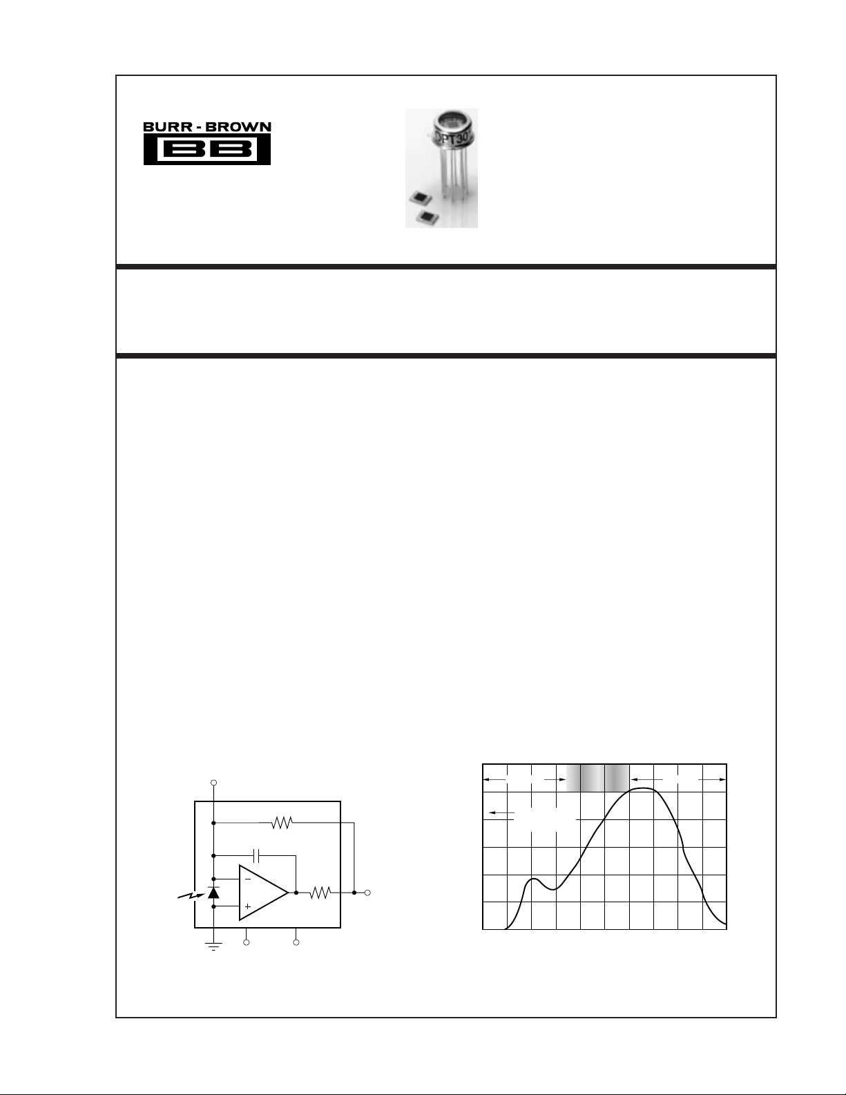
DESCRIPTION
The OPT301 is an opto-electronic integrated circuit
containing a photodiode and transimpedance
amplifier on a single dielectrically isolated chip. The
transimpedance amplifier consists of a precision FETinput op amp and an on-chip metal film resistor. The
0.09 x 0.09 inch photodiode is operated at zero bias for
excellent linearity and low dark current.
The integrated combination of photodiode and
transimpedance amplifier on a single chip eliminates
the problems commonly encountered in discrete designs such as leakage current errors, noise pick-up and
gain peaking due to stray capacitance.
The OPT301 operates over a wide supply range (±2.25
to ±18V) and supply current is only 400µA. It is
packaged in a hermetic TO-99 metal package with a
glass window, and is specified for the –40°C to 85°C
temperature range.
SPECTRAL RESPONSIVITY
0.5
0.4
0.3
Ultraviolet
Using Internal
1MΩ Resistor
Blue
Green
Yellow
Red
Infrared
0.5
0.4
0.3
75Ω
5
V
λ
OPT301
1
83
V+
International Airport Industrial Park • Mailing Address: PO Box 11400, Tucson, AZ 85734 • Street Address: 6730 S. Tucson Blvd., Tucson, AZ 85706 • Tel: (520) 746-1111 • Twx: 910-952-1111
Internet: http://www.burr-brown.com/ • FAXLine: (800) 548-6133 (US/Canada Only) • Cable: BBRCORP • Telex: 066-6491 • FAX: (520) 889-1510 • Immediate Product Info: (800) 548-6132
©
1994 Burr-Brown Corporation PDS-1228B Printed in U.S.A. January, 1994
V–
O
0.2
Voltage Output (V/µW)
0.1
0
100 200 300 400 500 600 700 800 900 1000 1100
Wavelength (nm)
0.2
0.1
Photodiode Responsivity (A/W)
0

SPECIFICATIONS
ELECTRICAL
At TA = +25°C, VS = ±15V, λ = 650nm, internal 1MΩ feedback resistor, unless otherwise noted.
OPT301M
PARAMETER CONDITIONS MIN TYP MAX UNITS
RESPONSIVITY
Photodiode Current 650nm 0.47 A/W
Voltage Output 650nm 0.47 V/µW
vs Temperature 200 ppm/°C
Unit-to-Unit Variation 650nm ±5%
Nonlinearity
Photodiode Area (0.090 x 0.090in) 0.008 in
DARK ERRORS, RTO
Offset Voltage, Output ±0.5 ±2mV
vs Temperature ±10 µV/°C
vs Power Supply V
Voltage Noise Measured BW = 0.1 to 100kHz 160 µVrms
RESISTOR—1MΩ Internal
Resistance 1MΩ
Tolerance ±0.5 ±2%
vs Temperature 50 ppm/°C
FREQUENCY RESPONSE
Bandwidth, Large or Small-Signal, –3dB 4 kHz
Rise Time, 10% to 90% 90 µs
Settling Time, 1% FS to Dark 240 µs
Overload Recovery Time 100% overdrive, V
OUTPUT
Voltage Output R
Capacitive Load, Stable Operation 10 nF
Short-Circuit Current ±18 mA
POWER SUPPLY
Specified Operating Voltage ±15 V
Operating Voltage Range ±2.25 ±18 V
Quiescent Current I
TEMPERATURE RANGE
Specification –40 +85 °C
Operating/Storage –55 +125 °C
Thermal Resistance,
NOTES: (1) Deviation in percent of full scale from best-fit straight line. (2) Referred to Output. Includes all error sources.
(1)
FS Output = 10V 0.01 % of FS
(2.29 x 2.29mm) 5.2 mm
(2)
= ±2.25V to ±18V 10 100 µV/V
S
0.1% FS to Dark 350 µs
0.01% FS to Dark 900 µs
= ±15V 240 µs
100% overdrive, V
100% overdrive, V
θ
JA
S
= ±5V 500 µs
S
= ±2.25V 1000 µs
S
= 10kΩ (V+) – 1.25 (V+) – 0.65 V
L
R
= 5kΩ (V+) – 2 (V+) – 1 V
L
= 0 ±0.4 ±0.5 mA
O
200 °C/W
2
2
PHOTODIODE SPECIFICATIONS
At TA = +25°C, unless otherwise noted.
Photodiode of OPT301
PARAMETER CONDITIONS MIN TYP MAX UNITS
Photodiode Area (0.090 x 0.090in) 0.008 in
Current Responsivity 650nm 0.47 A/W
Dark Current V
vs Temperature doubles every 10°C
Capacitance V
NOTE: (1) Voltage Across Photodiode.
®
OPT301
(2.29 x 2.29mm) 5.1 mm
(1)
= 0V
D
= 0V
D
(1)
500 fA
4000 pF
2
2
2

SPECIFICATIONS (CONT)
ELECTRICAL Op Amp Section of OPT301
At TA = +25°C, VS = ±15V, unless otherwise noted.
OPT301 Op Amp
PARAMETER CONDITIONS MIN TYP MAX UNITS
INPUT
Offset Voltage ±0.5 mV
vs Temperature ±5 µV/°C
vs Power Supply V
Input Bias Current 1pA
vs Temperature doubles every 10°C
NOISE
Input Voltage Noise
Voltage Noise Density, f=10Hz 30 nV/√Hz
f=100Hz 25 nV/√Hz
f=1kHz 15 nV/√Hz
Current Noise Density, f=1kHz 0.8 fA/√Hz
INPUT VOLTAGE RANGE
Common-Mode Input Range ±14.4 V
Common-Mode Rejection 106 dB
INPUT IMPEDANCE
Differential 10
Common-Mode 10
OPEN-LOOP GAIN
Open-Loop Voltage Gain 120 dB
FREQUENCY RESPONSE
Gain-Bandwidth Product 380 kHz
Slew Rate 0.5 V/µs
Settling Time 0.1% 4 µs
0.01% 5 µs
OUTPUT
Voltage Output R
Short-Circuit Current ±18 mA
POWER SUPPLY
Specified Operating Voltage ±15 V
Operating Voltage Range ±2.25 ±18 V
Quiescent Current I
NOTE: (1) Op amp specifications provided for information and comparison only.
= ±2.25V to ±18V 10 µV/V
S
12
||3 Ω||pF
12
||3 Ω||pF
= 10kΩ (V+) – 1.25 (V+) – 0.65 V
L
R
= 5kΩ (V+) – 2 (V+) – 1 V
L
= 0 ±0.4 ±0.5 mA
O
(1)
6
The information provided herein is believed to be reliable; however, BURR-BROWN assumes no responsibility for inaccuracies or omissions. BURR-BROWN assumes
no responsibility for the use of this information, and all use of such information shall be entirely at the user’s own risk. Prices and specifications are subject to change
without notice. No patent rights or licenses to any of the circuits described herein are implied or granted to any third party. BURR-BROWN does not authorize or warrant
any BURR-BROWN product for use in life support devices and/or systems.
3
OPT301
®
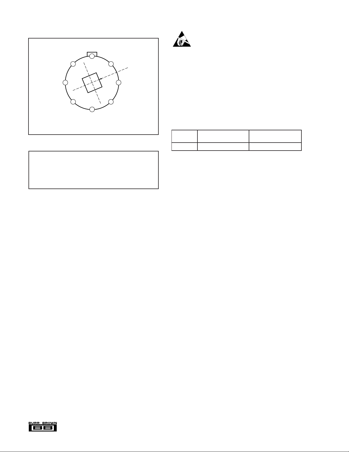
PIN CONFIGURATION
Top View
V+
26
V–
NOTE: Metal package is internally connected to common (Pin 8).
Common
8
1
3
4
1MΩ Feedback
NC
7
5
Output
Photodiode
Area
NC–In
ABSOLUTE MAXIMUM RATINGS
Supply Voltage................................................................................... ±18V
Input Voltage Range (Common Pin) .................................................... ±V
Output Short-Circuit (to ground)............................................... Continuous
Operating Temperature................................................... –55°C to +125°C
Storage Temperature...................................................... –55°C to +125°C
Junction Temperature .................................................................... +125°C
Lead Temperature (soldering, 10s)................................................ +300°C
ELECTROSTATIC
DISCHARGE SENSITIVITY
This integrated circuit can be damaged by ESD. Burr-Brown
recommends that all integrated circuits be handled with appropriate precautions. Failure to observe proper handling and
installation procedures can cause damage.
ESD damage can range from subtle performance degradation
to complete device failure. Precision integrated circuits may
be more susceptible to damage because very small parametric
changes could cause the device not to meet its published
specifications.
PACKAGE INFORMATION
PRODUCT PACKAGE NUMBER
OPT301M 8-Pin TO-99 001-1
NOTE: (1) For detailed drawing and dimension table, please see end of data
S
sheet, or Appendix C of Burr-Brown IC Data Book.
PACKAGE DRAWING
(1)
®
OPT301
4
 Loading...