

Burr Brown OPT101P-J, OPT101P Datasheet
®
OPT101
MONOLITHIC PHOTODIODE AND
SINGLE-SUPPLY TRANSIMPEDANCE AMPLIFIER
FEATURES
● SINGLE SUPPLY: +2.7 to +36V
● PHOTODIODE SIZE: 0.090 x 0.090 inch
● INTERNAL 1MΩ FEEDBACK RESISTOR
= 1MΩ
F
(650nm)
µA
● HIGH RESPONSIVITY: 0.45A/W
● BANDWIDTH: 14kHz at R
● LOW QUIESCENT CURRENT: 120
● AVAILABLE IN 8-PIN DIP, 5-PIN SIP, AND
8-LEAD SURFACE MOUNT PACKAGES
APPLICATIONS
● MEDICAL INSTRUMENTATION
● LABORATORY INSTRUMENTATION
● POSITION AND PROXIMITY SENSORS
● PHOTOGRAPHIC ANALYZERS
● BARCODE SCANNERS
● SMOKE DETECTORS
● CURRENCY CHANGERS
(Pin available
on DIP only.)
λ
2 (2)
(1)
7.5mV
V
B
V+
1
3pF
1MΩ
8pF
OPT101
(3)
3
8
(4)
54(5)
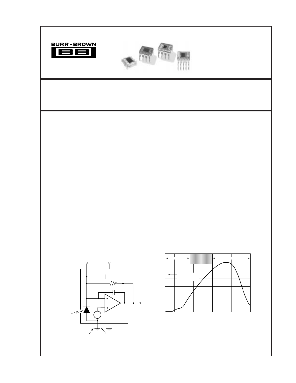
DESCRIPTION
The OPT101 is a monolithic photodiode with on-chip
transimpedance amplifier. Output voltage increases
linearly with light intensity. The amplifier is designed
for single or dual power supply operation, making it
ideal for battery operated equipment.
The integrated combination of photodiode and
transimpedance amplifier on a single chip eliminates
the problems commonly encountered in discrete designs such as leakage current errors, noise pick-up and
gain peaking due to stray capacitance. The 0.09 x 0.09
inch photodiode is operated in the photoconductive
mode for excellent linearity and low dark current.
The OPT101 operates from +2.7V to +36V supplies
and quiescent current is only 120µA. It is available in
clear plastic 8-pin DIP, 5-pin SIP and J-formed DIP for
surface mounting. Temperature range is 0°C to 70°C.
0.7
Ultraviolet
0.6
0.5
0.4
0.3
0.2
Voltage Output (V/µW)
0.1
0
200 300 400 500 600 700 800 900 1000 1100
SPECTRAL RESPONSIVITY
Blue
Green
Yellow
Using Internal
1MΩ Resistor
Wavelength (nm)
Red
Infrared
0.7
0.6
0.5
0.4
0.3
0.2
Photodiode Responsivity (A/W)
0.1
0
(SIP)
International Airport Industrial Park • Mailing Address: PO Box 11400, Tucson, AZ 85734 • Street Address: 6730 S. Tucson Blvd., Tucson, AZ 85706 • Tel: (520) 746-1111 • Twx: 910-952-1111
Internet: http://www.burr-brown.com/ • FAXLine: (800) 548-6133 (US/Canada Only) • Cable: BBRCORP • Telex: 066-6491 • FAX: (520) 889-1510 • Immediate Product Info: (800) 548-6132
©
1994 Burr-Brown Corporation PDS-1257D Printed in U.S.A. March, 1998
DIP
®
1
OPT101

SPECIFICATIONS
At TA = +25°C, VS = +2.7V to +36V, λ = 650nm, internal 1MΩ feedback resistor, and RL = 10kΩ, unless otherwise noted.
OPT101P, W
PARAMETER CONDITIONS MIN TYP MAX UNITS
RESPONSIVITY
Photodiode Current 650nm 0.45 A/W
Voltage Output 650nm 0.45 V/µW
vs Temperature 100 ppm/°C
Unit to Unit Variation 650nm ±5%
Nonlinearity
Photodiode Area (0.090 x 0.090in) 0.008 in
DARK ERRORS, RTO
Offset Voltage, Output +5 +7.5 +10 mV
vs Temperature ±2.5 µV/°C
vs Power Supply V
Voltage Noise, Dark, f
TRANSIMPEDANCE GAIN
Resistor 1MΩ
Tolerance, P ± 0.5 ± 2%
FREQUENCY RESPONSE
Bandwidth V
Rise Fall Time, 10% to 90% V
Settling Time, 0.05% V
Overload Recovery 100%, Return to Linear Operation 50 µs
OUTPUT
Voltage Output, High (V
Capacitive Load, Stable Operation 10 nF
Short-Circuit Current V
POWER SUPPLY
Operating Voltage Range +2.7 +36 V
Quiescent Current Dark, V
TEMPERATURE RANGE
Specification 0 +70 °C
Operating 0 +70 °C
Storage –25 +85 °C
Thermal Resistance,
NOTES: (1) Deviation in percent of full scale from best-fit straight line. (2) Referred to Output. Includes all error sources.
(1)
FS Output = 24V ±0.01 % of FS
2
(2.29 x 2.29mm) 5.2 mm
(2)
= +2.7V to +36V 10 100 µV/V
= 0.1Hz to 20kHz VS = +15V, V
B
S
= –15V 300 µVrms
PIN3
W ±0.5 %
vs Temperature ±50 ppm/°C
= 10Vp-p 14 kHz
OUT
= 10V Step 28 µs
OUT
= 10V Step 160 µs
0.1% 80 µs
OUT
1% 70 µs
) – 1.3 (VS) – 1.15 V
S
= 36V 15 mA
S
= 0V 120 240 µA
PIN3
R
= ∞, V
L
θ
JA
= 10V 220 µA
OUT
100 °C/W
2
PHOTODIODE SPECIFICATIONS
TA = +25°C, VS = +2.7V to +36V unless otherwise noted.
Photodiode of OPT101P
PARAMETER CONDITIONS MIN TYP MAX UNITS
Photodiode Area (0.090 x 0.090in) 0.008 in
(2.29 x 2.29mm) 5.2 mm
Current Responsivity 650nm 0.45 A/W
650nm 865 µA/W/cm
Dark Current V
vs Temperature doubles every 7°C
= 7.5mV 2.5 pA
DIODE
Capacitance 1200 pF
The information provided herein is believed to be reliable; however, BURR-BROWN assumes no responsibility for inaccuracies or omissions. BURR-BROWN assumes
no responsibility for the use of this information, and all use of such information shall be entirely at the user’s own risk. Prices and specifications are subject to change
without notice. No patent rights or licenses to any of the circuits described herein are implied or granted to any third party. BURR-BROWN does not authorize or warrant
any BURR-BROWN product for use in life support devices and/or systems.
®
OPT101
2
2
2
2

OP AMP SPECIFICATIONS
At TA = +25°C, VS = +2.7V to +36V, λ = 650nm, internal 1MΩ feedback resistor, and RL = 10kΩ, unless otherwise noted.
OPT101 Op Amp
PARAMETER CONDITIONS MIN TYP MAX UNITS
INPUT
Offset Voltage ±0.5 mV
vs Temperature ±2.5 µV/°C
vs Power Supply 10 µV/V
Input Bias Current (–) Input 165 pA
vs Temperature (–) Input 1 pA/°C
Input Impedance
Differential 400 || 5 MΩ || pF
Common-Mode 250 || 35 GΩ || pF
Common-Mode Input Voltage Range Linear Operation 0 to [(V
Common-Mode Rejection 90 dB
OPEN-LOOP GAIN
Open-loop Voltage Gain 90 dB
FREQUENCY RESPONSE
Gain-Bandwidth Product
(2)
Slew Rate 1V/µs
Settling Time 1% 5.8 µs
0.1% 7.7 µs
0.05% 8.0 µs
OUTPUT
Voltage Output, High (V
Short-Circuit Current V
= +36V 15 mA
S
– 1.3 (VS) – 1.15 V
S)
POWER SUPPLY
Operating Voltage Range +2.7 +36 V
Quiescent Current Dark, V
R
= 0V 120 240 µA
PIN3
∞, V
= 10V 220 µA
L
OUT
NOTES: (1) Op amp specifications provided for information and comparison only. (2) Stable gains ≥ 10V/V.
(1)
) – 1] V
S
2 MHz
®
3
OPT101
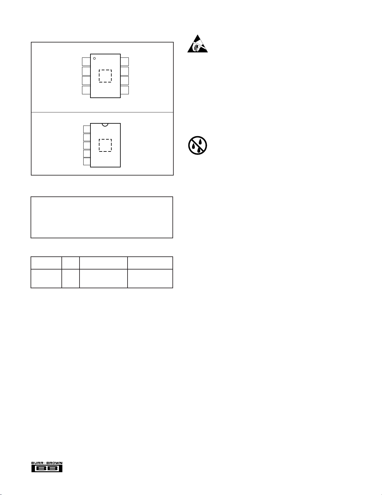
PIN CONFIGURATIONS
Top View DIP
ELECTROSTATIC
DISCHARGE SENSITIVITY
1
V
S
2
–In
–V
1MΩ Feedback
NOTE: (1) Photodiode location.
Top View SIP
Common
V
S
–V
1MΩ Feedback
Output
(1)
3
4
1
2
(1)
3
4
5
8
7
6
5
Common
NC
NC
Output
ABSOLUTE MAXIMUM RATINGS
Supply Voltage (VS to
Output Short-Circuit (to ground)............................................... Continuous
Operating Temperature..................................................... –25°C to +85°C
Storage Temperature........................................................ –25°C to +85°C
Junction Temperature ...................................................................... +85°C
Lead Temperature (soldering, 10s)................................................ +300°C
(Vapor-Phase Soldering Not Recommended)
“Common”
or pin 3) ................................0 to +36V
This integrated circuit can be damaged by ESD. Burr-Brown
recommends that all integrated circuits be handled with appropriate precautions. Failure to observe proper handling and
installation procedures can cause damage.
ESD damage can range from subtle performance degradation
to complete device failure. Precision integrated circuits may
be more susceptible to damage because very small parametric
changes could cause the device not to meet its published
specifications.
MOISTURE SENSITIVITY
AND SOLDERING
Clear plastic does not contain the structural-enhancing fillers
used in black plastic molding compound. As a result, clear
plastic is more sensitive to environmental stress than black
plastic. This can cause difficulties if devices have been stored
in high humidity prior to soldering. The rapid heating during
soldering can stress wire bonds and cause failures. Prior to
soldering, it is recommended that plastic devices be baked-out
at +85°C for 24 hours.
The fire-retardant fillers used in black plastic are not compatible with clear molding compound. The OPT101 plastic
packages cannot meet flammability test, UL-94.
PACKAGE INFORMATION
PRODUCT COLOR PACKAGE NUMBER
OPT101P Clear 8-Pin Plastic DIP 006-1
OPT101P-J Clear 8-Lead Surface Mount
OPT101W Clear 5-Pin Plastic SIP 321
NOTE: (1) For detailed drawing and dimension table, please see end of data
sheet, or Appendix C of Burr-Brown IC Data Book. (2) 8-pin DIP with J-formed
leads for surface mounting.
PACKAGE DRAWING
(2)
(1)
006-4
®
OPT101
4
 Loading...