

Burr Brown OPA688U-2K5, OPA688U, OPA688P Datasheet
1
®
OPA688
Unity Gain Stable, Wideband
VOLTAGE LIMITING AMPLIFIER
OPA688
®
FEATURES
● HIGH LINEARITY NEAR LIMITING
● FAST RECOVERY FROM OVERDRIVE: 2.4ns
● LIMITING VOLTAGE ACCURACY: ±15mV
● –3dB BANDWIDTH (G = +1): 530MHz
● SLEW RATE: 1000V/µs
● ±5V AND 5V SUPPLY OPERATION
● HIGH GAIN VERSION: OPA689
APPLICATIONS
● FAST LIMITING ADC INPUT BUFFER
● CCD PIXEL CLOCK STRIPPING
● VIDEO SYNC STRIPPING
● HF MIXER
● IF LIMITING AMPLIFIER
● AM SIGNAL GENERATION
● NON-LINEAR ANALOG SIGNAL PROCESSING
● COMPARATOR
DESCRIPTION
The OPA688 is a wideband, unity gain stable voltage
feedback op amp that offers bipolar output voltage limiting. Two buffered limiting voltages take control of the
output when it attempts to drive beyond these limits.
This new output limiting architecture holds the limiter
offset error to ±15mV. The op amp operates linearly to
within 30mV of the output limit voltages.
The combination of narrow nonlinear range and low
limiting offset allows the limiting voltages to be set
within 100mV of the desired linear output range. A fast
2.4ns recovery from limiting ensures that overdrive signals will be transparent to the signal channel. Implementing the limiting function at the output, as opposed to
the input, gives the specified limiting accuracy for any
gain, and allows the OPA688 to be used in all standard
op amp applications.
Non-linear analog signal processing will benefit from
the OPA688’s sharp transition from linear operation to
output limiting. The quick recovery time supports high
speed applications.
The OPA688 is available in an industry standard pinout
in PDIP-8 and SO-8 packages. For higher gain, or
transimpedance applications requiring output limiting
with fast recovery, consider the OPA689.
©
1997 Burr-Brown Corporation PDS-1424D Printed in U.S.A. January, 2000
TM
OPA688
OPA688
2.5
2.0
1.5
1.0
0.5
0
–0.5
–1.0
–1.5
–2.0
–2.5
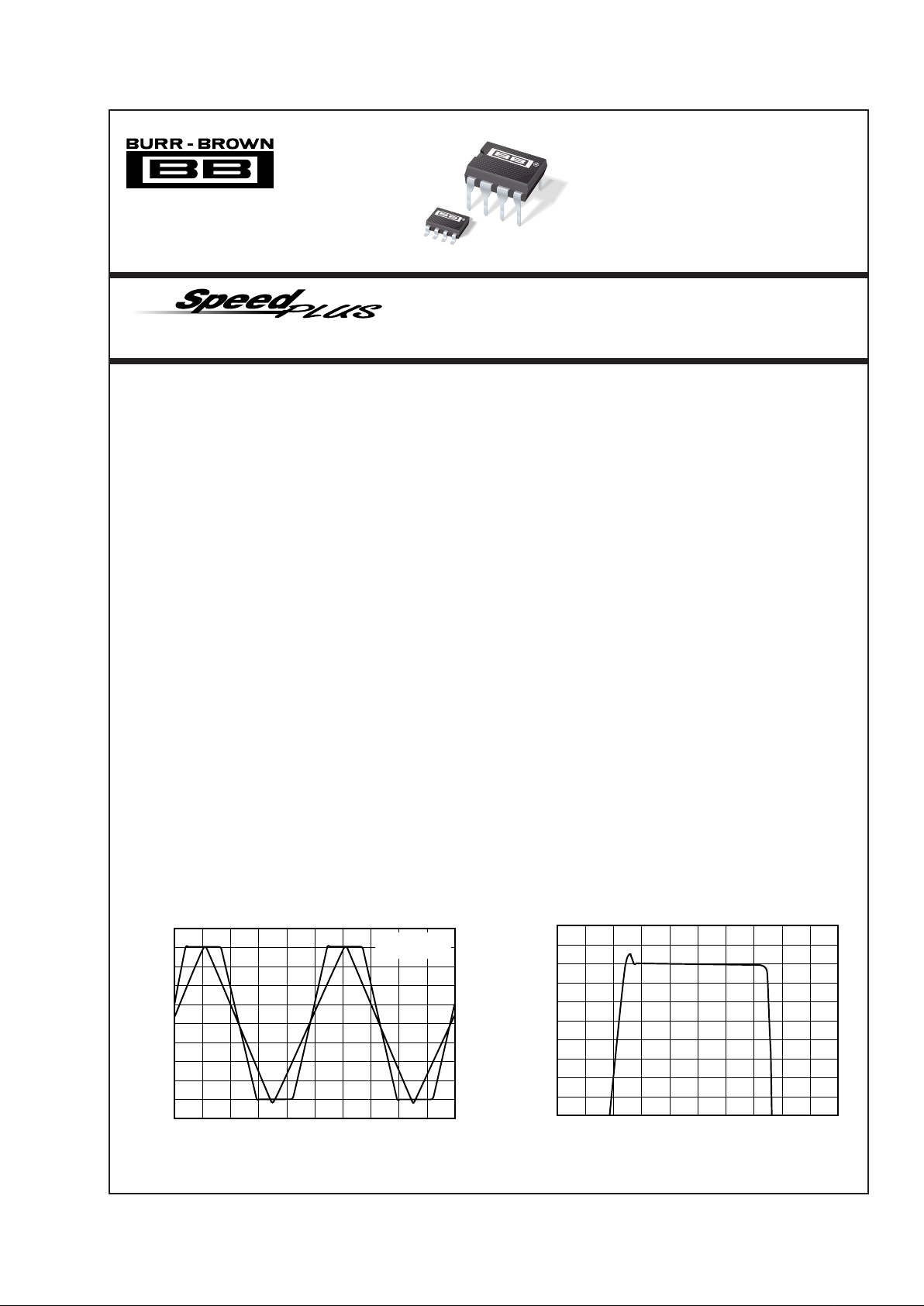
LIMITED OUTPUT RESPONSE
V
INVO
Time (200ns/div)
Input and Output Voltage (V)
VH = –VL = 2.0V
G = +2
2.10
2.05
2.00
1.95
1.90
1.85
1.80
1.75
1.70
1.65
1.60
DETAIL OF LIMITED OUTPUT VOLTAGE
Time (50ns/div)
V
O
Output Voltage (V)
For most current data sheet and other product
information, visit www.burr-brown.com
International Airport Industrial Park • Mailing Address: PO Box 11400, Tucson, AZ 85734 • Street Address: 6730 S. Tucson Blvd., Tucson, AZ 85706 • Tel: (520) 746-1111
Twx: 910-952-1111 • Internet: http://www.burr-brown.com/ • Cable: BBRCORP • Telex: 066-6491 • FAX: (520) 889-1510 • Immediate Product Info: (800) 548-6132
2
®
OPA688
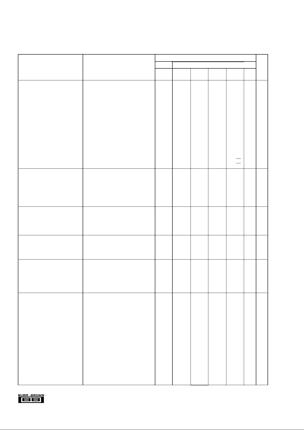
AC PERFORMANCE (see Figure 1)
Small Signal Bandwidth V
O
< 0.2Vp-p
G = +1, R
F
= 25Ω 530 — — — MHz Typ C
G = +2 260 150 140 135 MHz Min B
G = –1 230 — — — MHz Typ C
Gain-Bandwidth Product (G ≥ +5) V
O
< 0.2Vp-p 290 175 170 160 MHz Min B
Gain Peaking G = +1, R
F
= 25Ω, VO < 0.2Vp-p 11 — —
—
dB Typ C
0.1dB Gain Flatness Bandwidth V
O
< 0.2Vp-p 50 — — — MHz Typ C
Large Signal Bandwidth V
O
= 4Vp-p, VH = –VL = 2.5V 145 100 95 90 MHz Min B
Step Response:
Slew Rate 4V Step, V
H
= –VL = 2.5V 1000 800 770 650 V/µs Min B
Rise/Fall Time 0.2V Step 1.2 2.6 2.7 3 ns Max B
Settling Time: 0.05% 2V Step 7 ———nsTypC
Spurious Free Dynamic Range f = 5MHz, V
O
= 2Vp-p 66 62 58 53 dB Min B
Differential Gain NTSC, PAL, R
L
= 500Ω 0.02 — — — % Typ C
Differential Phase NTSC, PAL, R
L
= 500Ω 0.01 — — — ° Typ C
Input Noise:
Voltage Noise Density f ≥ 1MHz 6.3 7.2 7.8 8 nV/√Hz Max B
Current Noise Density f ≥ 1MHz 2.0 2.5 2.9 3.6 pA/√Hz Max B
DC PERFORMANCE (V
CM
= 0)
Open Loop Voltage Gain (A
OL
)V
O
= ±0.5V 52 46 44 43 dB Min A
Input Offset Voltage ±2
±6 ±7 ±9 mV Max A
Average Drift ——±14 ±14 µV/°C Max B
Input Bias Current
(3)
+6 ±12 ±13 ±20 µA Max A
Average Drift — — –60 –90 nA/°C Max B
Input Offset Current ±0.3
±2 ±3 ±4 µA Max A
Average Drift ——±10 ±10 nA/°C Max B
INPUT
Common-Mode Rejection Input Referred, V
CM
= ±0.5V 57 50 49 47 dB Min A
Common-Mode Input Range
(4)
±3.3 ±3.2 ±3.2 ±3.1 V Min A
Input Impedance
Differential-Mode 0.4 || 1 — — — MΩ || pF Typ C
Common-Mode 1 || 1 — — — MΩ || pF Typ C
OUTPUT V
H
= –VL = 4.3V
Output Voltage Range R
L
≥ 500Ω±4.1 ±3.9 ±3.9 ±3.8 V Min A
Current Output, Sourcing V
O
= 0 105 90 85 80 mA Min A
Sinking V
O
= 0 –85 –70 –65 –60 mA Min A
Closed-Loop Output Impedance G = +1, R
F
= 25Ω, f < 100kHz 0.2 — — — Ω Typ C
POWER SUPPLY
Operating Voltage, Specified ±5———VTypC
Maximum — ±6 ±6 ±6 V Max A
Quiescent Current, Maximum 15.8 17 19 20 mA Max A
Minimum 15.8 14 12.8 11 mA Min A
Power Supply Rejection Ratio +V
S
= 4.5V to 5.5V
+PSR (Input Referred) 65 58 57 55 dB Min A
OUTPUT VOLTAGE LIMITERS Pins 5 and 8
Default Limit Voltage Limiter Pins Open ±3.3
±3.0 ±3.0 ±2.9 V Min A
Minimum Limiter Separation (V
H
– VL) 200 200 200 200 mV Min B
Maximum Limit Voltage — ±4.3 ±4.3 ±4.3 V Max B
Limiter Input Bias Current Magnitude
(5)
VO = 0
Maximum 54 65 68 70 µA Max A
Minimum 54 35 34 31 µA Min A
Average Drift — — 40 45 nA/°C Max B
Limiter Input Impedance 2 || 1 — — — MΩ || pF Typ C
Limiter Feedthrough
(6)
f = 5MHz –60 — — — dB Typ C
DC Performance in Limit Mode V
IN
= ±2V
Limiter Offset (V
O
– VH) or (VO – VL) ±15 ±35 ±40 ±40 mV Max A
Op Amp Input Bias Current Shift
(3)
3———µA Typ C
AC Performance in Limit Mode
Limiter Small Signal Bandwidth V
IN
= ±2V, VO < 0.02Vp-p 450 — — — MHz Typ C
Limiter Slew Rate
(7)
100 — — — V/µs Typ C
Limited Step Response 2x Overdrive
Overshoot V
IN
= 0 to ±2V Step 250 — — — mV Typ C
Recovery Time V
IN
= ±2V to 0V Step 2.4 2.8 3.0 3.2 ns Max B
Linearity Guardband
(8)
f = 5MHz, VO = 2Vp-p 30 — — — mV Typ C
SPECIFICATIONS—VS = ±5V
G = +2, RL = 500Ω, RF = 402Ω, VH = –VL = 2V (Figure 1 for AC performance only), unless otherwise noted.
OPA688U, P
TYP GUARANTEED
(1)
0°C to –40°C to
MIN/
TEST
PARAMETER CONDITIONS +25°C +25°C +70°C +85°C UNITS MAX
LEVEL
(2)
3
®
OPA688
THERMAL CHARACTERISTICS
Temperature Range Specification: P, U
–40 to +85
———°C Typ C
Thermal Resistance Junction-to-Ambient
P 8-Pin DIP 100 — — — °C/W Typ C
U 8-Pin SO-8 125 — — — °C/W Typ C
NOTES: (1) Junction Temperature = Ambient Temperature for low temperature limit and 25°C guaranteed specifications. Junction Temperature = Ambient Temperature
+ 23°C at high temperature limit guaranteed specifications. (2) TEST LEVELS: (A) 100% tested at 25°C. Over temperature limits by characterization and simulation.
(B) Limits set by characterization and simulation. (C) Typical value for information only. (3) Current is considered positive out of node. (4) CMIR tested as < 3dB
degradation from minimum CMRR at specified limits. (5) I
VH
(VH bias current) is positive, and IVL (VL bias current) is negative, under these conditions. See Note 3,
Figure 1 and Figure 8 . (6) Limiter feedthrough is the ratio of the output magnitude to the sinewave added to V
H
(or VL) when VIN = 0. (7) VH slew rate conditions are:
V
IN
= +2V, G = +2, VL = –2V, VH = step between 2V and 0V. VL slew rate conditions are similar. (8) Linearity Guardband is defined for an output sinusoid (f = 5MHz,
V
O
= 0VDC ±1Vp-p) centered between the limiter levels (VH and VL). It is the difference between the limiter level and the peak output voltage where SFDR decreases
by 3dB (see Figure 9).
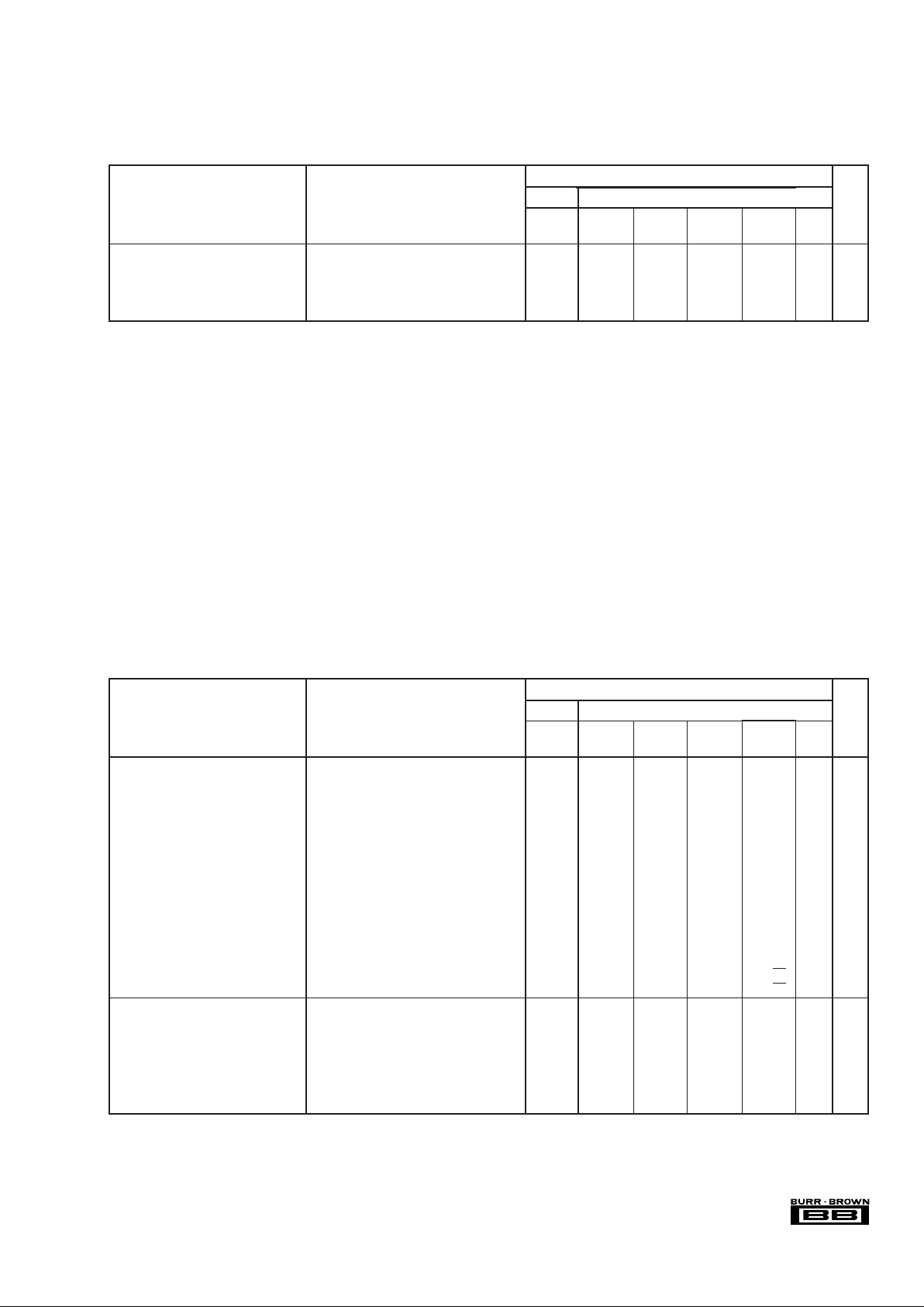
SPECIFICATIONS—VS = ±5V (CONT)
G = +2, RL = 500Ω, RF = 402Ω, VH = –VL = 2V (Figure 1 for AC performance only), unless otherwise noted.
OPA688U, P
TYP GUARANTEED
(1)
0°C to –40°C to
MIN/
TEST
PARAMETER CONDITIONS +25°C +25°C +70°C +85°C UNITS MAX
LEVEL
(2)
AC PERFORMANCE (see Figure 2)
Small Signal Bandwidth V
O
< 0.2Vp-p
G = +1, R
F
= 25Ω 515 — — — MHz Typ C
G = +2 240 110 105 100 MHz Min B
G = –1 190 — — — MHz Typ C
Gain-Bandwidth Product (G ≥ +5) V
O
< 0.2Vp-p 275 130 125 120 MHz Min B
Gain Peaking G = +1, R
F
= 25Ω, VO < 0.2Vp-p 10 — — — dB Typ C
0.1dB Gain Flatness Bandwidth V
O
< 0.2Vp-p 50 — — — MHz Typ C
Large Signal Bandwidth V
O
= 2Vp-p 240 110 105 100 MHz Min B
Step Response:
Slew Rate 2V Step 1000 800 770 650 V/µs Min B
Rise/Fall Time 0.2V Step 2.3 2.6 2.7 3 ns Max B
Settling Time: 0.05% 1V Step 12 ———nsTypC
Spurious Free Dynamic Range f = 5MHz, V
O
= 2Vp-p 64 60 56 51 dB Min B
Input Noise:
Voltage Noise Density f ≥ 1MHz 6.3 7.2 7.8 8 nV/√Hz Max B
Current Noise Density f ≥ 1MHz 2.0 2.5 2.9 3.6 pA/√Hz Max B
DC PERFORMANCE V
CM
= 2.5V
Open Loop Voltage Gain (A
OL
)V
O
= ±0.5V 52 46 44 43 dB Min A
Input Offset Voltage ±2
±6 ±7 ±9 mV Max A
Average Drift ——±14 ±14 µV/°C Max B
Input Bias Current
(3)
+6 ±12 ±13 ±20 µA Max A
Average Drift — — –60 –90 nA/°C Max B
Input Offset Current ±0.3
±2 ±3 ±4 µA Max A
Average Drift ——±10 ±10 nA/°C Max B
SPECIFICATIONS—VS = +5V
G = +2, RL = 500Ω tied to VCM = 2.5V, RF = 402Ω, VL = V
CM
–1.2V, VH = V
CM
+1.2V (Figure 2 for AC performance only), unless otherwise noted.
OPA688U, P
TYP GUARANTEED
(1)
0°C to –40°C to
MIN/
TEST
PARAMETER CONDITIONS +25°C +25°C +70°C +85°C UNITS MAX
LEVEL
(2)
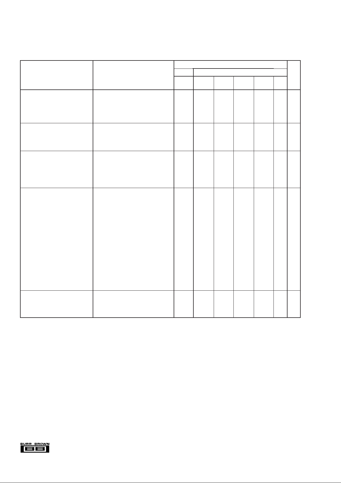
4
®
OPA688
INPUT
Common-Mode Rejection Input Referred, V
CM
= ±0.5V 55 48 47 45 dB Min A
Common-Mode Input Range
(4)
VCM ±0.8 VCM ±0.7 VCM ±0.7 VCM ±0.6 V Min A
Input Impedance
Differential-Mode 0.4 || 1 — — — MΩ || pF Typ C
Common-Mode 1 || 1 — — — MΩ || pF Typ C
OUTPUT V
H
= VCM +1.8V, VL = = VCM –1.8V
Output Voltage Range R
L
≥ 500Ω VCM ±1.6 VCM ±1.4 VCM ±1.4 VCM ±1.3 V Min A
Current Output, Sourcing V
O
= 2.5V 70 60 55 50 mA Min A
Sinking V
O
= 2.5V –60 –50 –45 –40 mA Min A
Closed-Loop Output Impedance G = +1, R
F
= 25Ω, f < 100kHz 0.2 — — — Ω Typ C
POWER SUPPLY Single Supply Operation
Operating Voltage, Specified +5 — — — V Typ C
Maximum — +12 +12 +12 V Max A
Quiescent Current, Maximum 13 15 15 16 mA Max A
Minimum 13 11 10 9 mA Min A
Power Supply Rejection Ratio V
S
= 4.5V to 5.5V
+PSR (Input Referred) 65 — — — dB Typ C
OUTPUT VOLTAGE LIMITERS Pins 5 and 8
Default Limiter Voltage Limiter Pins Open V
CM
±0.9 VCM ±0.6 VCM ±0.6 VCM ±0.6 V Min A
Minimum Limiter Separation (V
H
– VL) 200 200 200 200 mV Min B
Maximum Limit Voltage — V
CM
±1.8 VCM ±1.8 VCM ±1.8 V Max B
Limiter Input Bias Current Magnitude
(5)
VO = 2.5V
Maximum 35 65 75 85 µA Max A
Minimum 35 0 00µA Min A
Average Drift — — 30 50 nA/°C Max B
Limiter Input Impedance 2 || 1 — — — MΩ || pF Typ C
Limiter Feedthrough
(6)
f = 5MHz –60 — — — dB Typ C
DC Performance in Limit Mode V
IN
= VCM ±1.2V
Limiter Voltage Accuracy (V
O
– VH) or (VO – VL) ±15 ±35 ±40 ±40 mV Max A
Op Amp Bias Current Shift
(3)
5———µA Typ C
AC Performance in Limit Mode
Limiter Small Signal Bandwidth V
IN
= VCM ±1.2V, VO < 0.02Vp-p 300 — — — MHz Typ C
Limiter Slew Rate
(7)
20———V/µs Typ C
Limited Step Response 2x Overdrive
Overshoot V
IN
= VCM to V
CM
±1.2V Step 55 — — — mV Typ C
Recovery Time V
IN
= VCM ±1.2V to VCM Step 15 ———nsMaxC
Linearity Guardband
(8)
f = 5MHz, VO = 2Vp-p 30 — — — mV Max C
THERMAL CHARACTERISTICS
Temperature Range Specification: P, U
–40 to +85
———°C Typ C
Thermal Resistance Junction-to-Ambient
P 8-Pin DIP 100 — — — °C/W Typ C
U 8-Pin SO-8 125 — — — °C/W Typ C
NOTES: (1) Junction Temperature = Ambient Temperature for low temperature limit and 25°C guaranteed specifications. Junction Temperature = Ambient
Temperature + 23°C at high temperature limit guaranteed specifications. (2) TEST LEVELS: (A) 100% tested at 25 °C. Over temperature limits by characterization
and simulation. (B) Limits set by characterization and simulation. (C) Typical value for information only. (3) Current is considered positive out of node. (4) CMIR
tested as < 3dB degradation from minimum CMRR at specified limits. (5) I
VH
(VH bias current) is negative, and IVL (VL bias current) is positive, under these conditions.
See Note 3, Figures 2, and Figure 8. (6) Limiter feedthrough is the ratio of the output magnitude to the sinewave added to V
H
(or VL) when VIN = 0. (7) VH slew
rate conditions are: V
IN
= V
CM
+0.4V, G = +2, VL = V
CM
–1.2V, VH = step between VCM + 1.2V and VCM. VL slew rate conditions are similar. (8) Linearity Guardband
is defined for an output sinusoid (f = 5MHz, V
O
= V
CM
±1Vp-p) centered between the limiter levels (VH and VL). It is the difference between the limiter level and the
peak output voltage where SFDR decreases by 3dB (see Figure 9).
SPECIFICATIONS—VS = +5V (CONT)
G = +2, RL = 500Ω tied to VCM = 2.5V, RF = 402Ω, VL = –1.2V, VH = +1.2V (Figure 2 for AC performance only), unless otherwise noted.
OPA688U, P
TYP GUARANTEED
(1)
0°C to –40°C to
MIN/
TEST
PARAMETER CONDITIONS +25°C +25°C +70°C +85°C UNITS MAX
LEVEL
(2)
5
®
OPA688
ABSOLUTE MAXIMUM RATINGS
Supply Voltage ................................................................................. ±6.5V
Internal Power Dissipation .......................... See Thermal Characteristics
Common-Mode Input Voltage ............................................................. ±V
S
Differential Input Voltage ..................................................................... ±V
S
Limiter Voltage Range........................................................... ±(VS – 0.7V)
Storage Temperature Range: P, U ................................–40°C to +125°C
Lead Temperature (DIP, soldering, 10s) ..................................... +300°C
(SO-8, soldering, 3s) ...................................... +260°C
Junction Temperature .................................................................... +175°C
The information provided herein is believed to be reliable; however, BURR-BROWN assumes no responsibility for inaccuracies or omissions. BURR-BROWN assumes
no responsibility for the use of this information, and all use of such information shall be entirely at the user’s own risk. Prices and specifications are subject to change
without notice. No patent rights or licenses to any of the circuits described herein are implied or granted to any third party. BURR-BROWN does not authorize or warrant
any BURR-BROWN product for use in life support devices and/or systems.
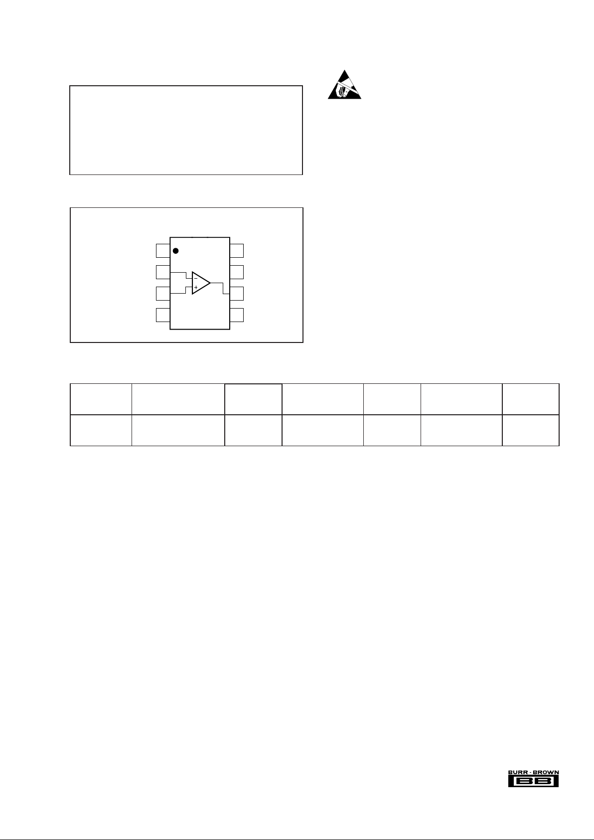
PIN CONFIGURATION
Top View DIP-8, SO-8
ELECTROSTATIC
DISCHARGE SENSITIVITY
Electrostatic discharge can cause damage ranging from performance degradation to complete device failure. Burr-Brown Corporation recommends that all integrated circuits be handled and stored
using appropriate ESD protection methods.
ESD damage can range from subtle performance degradation to
complete device failure. Precision integrated circuits may be more
susceptible to damage because very small parametric changes
could cause the device not to meet published specifications.
1
2
3
4
8
7
6
5
NC
Inverting Input
Non-Inverting Input
–V
S
V
H
+V
S
Output
V
L
PACKAGE SPECIFIED
DRAWING TEMPERATURE PACKAGE ORDERING TRANSPORT
PRODUCT PACKAGE NUMBER RANGE MARKING NUMBER
(1)
MEDIA
OPA688P DIP-8 Plastic DIP 006 –40°C to +85°C OPA688P OPA688P Rails
OPA688U SO-8 Surface Mount 182 –40°C to +85°C OPA688U OPA688U Rails
"""""OPA688U/2K5 Tape and Reel
NOTES: (1) Models with a slash (/) are available only in Tape and Reel in the quantities indicated (e.g., /2K5 indicates 2500 devices per reel). Ordering 2500 pieces
of OPA688U/2K5” will get a single 2500-piece Tape and Reel.
PACKAGE/ORDERING INFORMATION
 Loading...