

Burr Brown OPA687U, OPA687N-250, OPA687U-2K5, OPA687N-3K Datasheet
1
®
OPA687
OPA687
®
©
1998 Burr-Brown Corporation PDS-1372C Printed in U.S.A. May, 2000
Wideband, Ultra-Low Noise,
Voltage Feedback OPERATIONAL AMPLIFIER
With Power Down
FEATURES
● HIGH GAIN BANDWIDTH: 3.8GHz
● LOW INPUT VOLTAGE NOISE: 0.95nV/√Hz
● VERY LOW DISTORTION: –95dBc (5MHz)
● LOW DISABLED POWER: 2mW
● VERY HIGH SLEW RATE: 900V/µs
● STABLE FOR G ≥ 12
DESCRIPTION
The OPA687 combines a very high gain bandwidth and
large signal performance with an ultra-low input noise
voltage (0.95nV/√Hz) while dissipating only 18mA supply current. Where power savings is paramount, the
OPA687 also includes an optional power down pin that,
when pulled low, will disable the amplifier and decrease
the quiescent current to only 1% of its powered up value.
This optional feature may be left disconnected to insure
normal amplifier operation when no power-down is required.
The combination of low input voltage and current noise,
along with a 3.8GHz gain bandwidth product, make the
OPA687 an ideal amplifier for wideband transimpedance
APPLICA TIONS
● LOW DISTORTION ADC DRIVER
● OC-3 FIBER OPTIC RECEIVER
● LOW NOISE DIFFERENTIAL AMPLIFIERS
● EQUALIZING RECEIVERS
● ULTRASOUND CHANNEL AMPLIFIERS
● IMPROVED REPLACEMENT FOR THE
CLC425
TM
stages. As a voltage gain stage, the OPA687 is optimized for a flat frequency response at a gain of +20 and
is guaranteed stable down to gains of +12. New external
compensation techniques allows the OPA687 to be used
at any inverting gain with excellent frequency response
control. Using this compensation can give an extremely
high dynamic range ADC driver to support > 40MSPS
12- and 14-bit converters.
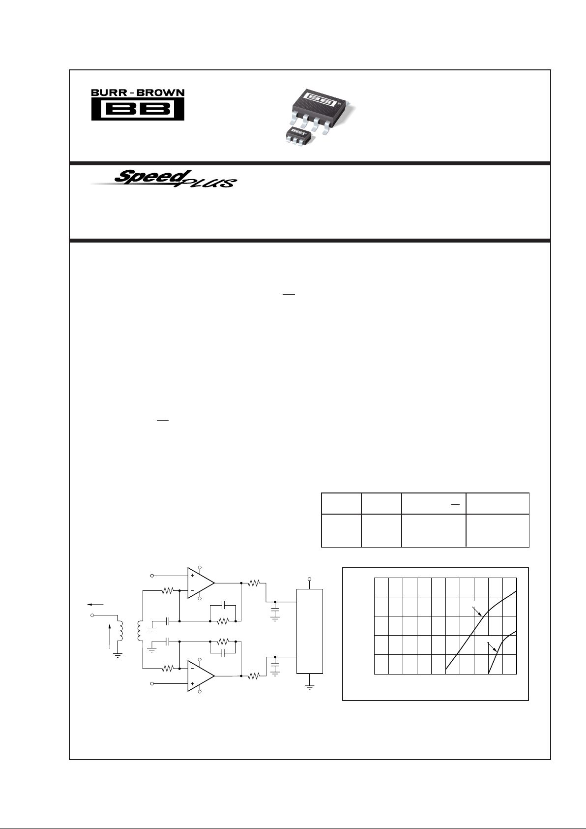
Ultra-High Dynamic Range
Differential Input ADC Driver
+5V
–5V
OPA687
+5V
+5V
–5V
850Ω
39pF
OPA687
1.7pF
80pF
V
IN
+
V
IN
–
80pF
1.7pF
850Ω
39pF
100Ω
20Ω
20Ω
1:2
50Ω Source
< 6dB
Noise
Figure
ADS852
14-Bit
65MSPS
100Ω
V
CM
V
CM
OPA687
IInternational Airport Industrial Park • Mailing Address: PO Box 11400, Tucson, AZ 85734 • Street Address: 6730 S. Tucson Blvd., Tucson, AZ 85706 • Tel: (520) 746-1111
Twx: 910-952-1111 • Internet: http://www.burr-brown.com/ • Cable: BBRCORP • Telex: 066-6491 • FAX: (520) 889-1510 • Immediate Product In
Center Frequency (MHz)
3rd-Order Spurious (dBc)
0
–60
–65
–70
–75
–80
–85
5101520253035404550
4Vp-p
2Vp-p
Measured 2-Tone, 3rd-Order Distortion for
Differential ADC Driver.
OPA687 RELATED PRODUCTS
INPUT NOISE GAIN BANDWIDTH
SINGLES DUAL VOLTAGE (nV/√Hz) PRODUCT (MHz)
OPA642 2.7 210
OPA643 2.3 800
OPA686 OPA2686 1.3 1600
For most current data sheet and other product
information, visit www.burr-brown.com
2
®
OPA687
OPA687U, N
TYP GUARANTEED
0°C to –40°C to
MIN/
TEST
PARAMETER CONDITIONS +25°C +25°C
(2)
70°C
(3)
+85°C
(3)
UNITS MAX
LEVEL
(1)
SPECIFICATIONS: VS = ±5V
RL = 100Ω, RF = 750Ω, and RG = 39.2Ω, G = +20 (Figure 1 for AC performance only), unless otherwise noted.
NOTES: (1) Test Levels: (A) 100% tested at 25°C. Over temperature limits by characterization and simulation. (B) Limits set by characterization and simulation.
(C) Typical value only for information. (2) Junction temperature = ambient for +25°C guaranteed specifications. (3) Junction temperature = ambient at low temperature
limit: junction temperature = ambient +23°C at high temperature limit for over temperature guaranteed specifications. (4) Current is considered positive out of node. V
CM
is the input common-mode voltage. (5) Tested <3dB below minimum specified CMRR at ±CMIR limits.
AC PERFORMANCE (Figure 1)
Closed-Loop Bandwidth G = +12, R
G
= 39.2Ω, VO = 200mVp-p 600 MHz typ C
G = +20, R
G
= 39.2Ω, VO = 200mVp-p 290 180 160 140 MHz min B
G = +50, R
G
= 39.2Ω, VO = 200mVp-p 75 60 54 48 MHz min B
Gain Bandwidth Product G ≥ +50 3800 3000 2700 2400 MHz min B
Bandwidth for 0.1dB Gain Flatness G = +20, R
L
= 100Ω 35 24 20 18 MHz min B
Peaking at a Gain of +12 3 8 10 14 dB max B
Harmonic Distortion G = +20, f = 5MHz, V
O
= 2Vp-p
2nd Harmonic R
L
= 100Ω –74 –70 –68 –65 dBc max B
R
L
= 500Ω –95 –90 –88 –85 dBc max B
3rd Harmonic R
L
= 100Ω –108 –95 –90 –85 dBc max B
R
L
= 500Ω –110 –105 –100 –95 dBc max B
Two-Tone, 3rd-Order Intercept G = +20, f = 20MHz 43 40 39 37 dBm min B
Input Voltage Noise Density f > 1MHz 0.95 1.1 1.15 1.3 nV/√Hz max B
Input Current Noise Density f > 1MHz 2.5 3.2 3.3 3.5 pA/√Hz max B
Pulse Response
Rise/Fall Time 0.2V Step 1.2 2.0 2.2 2.5 ns max B
Slew Rate 2V Step 900 675 550 450 V/µs min B
Settling Time to 0.01% 2V Step 17 ns typ C
0.1% 2V Step 15 18 20 25 ns max B
1% 2V Step 8 11 13 17 ns max B
DC PERFORMANCE
(4)
Open-Loop Voltage Gain (AOL)V
O
= 0V 85 78 75 70 dB min A
Input Offset Voltage V
CM
= 0V ±0.1 ±1 ±1.2 ±1.6 mV max A
Average Offset Voltage Drift V
CM
= 0V 5 10 µV/°C max B
Input Bias Current V
CM
= 0V –20 –33 –36 –40 µA max A
Input Bias Current Drift (magnitude) V
CM
= 0V –50 –100 nA/°C max B
Input Offset Current V
CM
= 0V ±0.2 ±1.0 ±1.5 ±1.8 µA max A
Input Offset Current Drift V
CM
= 0V ±12 ±15 nA/°C max B
INPUT
Common-Mode Input Range (CMIR)
(5)
±3.2 ±3.0 ±2.9 ±2.8 V min A
Common-Mode Rejection Ratio (CMRR) V
CM
= ±0.5V, Input Referred 100 88 83 78 dB min A
Input Impedance
Differential V
CM
= 0V 2.5 || 2.5 kΩ || pF typ C
Common-Mode V
CM
= 0V 1.0 || 1.2 MΩ || pF typ C
OUTPUT
Output Voltage Swing ≥ 400Ω Load ±3.6
±3.3 ±3.1 ±3.0 V min A
100Ω Load ±3.5
±3.2 ±2.9 ±2.8 V min A
Current Output, Sourcing V
O
= 0V 80 60 50 40 mA min A
Current Output, Sinking V
O
= 0V –80 –60 –50 –40 mA min A
Closed-Loop Output Impedance G = +20, f = < 100kHz 0.006 Ω typ C
POWER SUPPLY
Specified Operating Voltage ±5 V typ C
Maximum Operating Voltage ±6
±6 ±6 ±6 V max A
Quiescent Current, max V
S
= ±5V 18.5 19 19.5 20.5 mA max A
Quiescent Current, min V
S
= ±5V 18.5 18 17.5 16 mA min A
Power Supply Rejection Ratio
+PSRR, –PSRR |V
S
| = 4.5V to 5.5V, Input Referred 85 80 78 75 dB min A
POWER-DOWN (Disabled Low) (Pin 8 SO-8; Pin 5 on SOT23-6)
Power-Down Quiescent Current (+V
S
) –225 –300 –350 –400 µA max A
On Voltage (Enabled High or Floated) 3.3 3.5 3.6 3.7 V min A
Off Voltage (Disabled Asserted Low) 1.8 1.7 1.6 1.5 V max A
Power-Down Pin Input Bias Current (V
DIS
= 0) 100 160 160 160 µA max A
Power-Down Time 200 ns typ C
Power-Up Time 60 ns typ C
Off Isolation 5MHz, Input to Output 70 dB typ C
THERMAL
Specification U, N
–40 to +85
°C typ C
Thermal Resistance,
θ
JA
Junction to Ambient
U 8-Pin, SO-8 125 °C/W typ C
N 6-Pin, SOT23 150 °C/W typ C
3
®
OPA687
The information provided herein is believed to be reliable; however, BURR-BROWN assumes no responsibility for inaccuracies or omissions. BURR-BROWN assumes no responsibility for the use of this
information, and all use of such information shall be entirely at the user’s own risk. Prices and specifications are subject to change without notice. No patent rights or licenses to any of the circuits described
herein are implied or granted to any third party. BURR-BROWN does not authorize or warrant any BURR-BROWN product for use in life support devices and/or systems.
PACKAGE SPECIFIED
DRAWING TEMPERATURE PACKAGE ORDERING TRANSPORT
PRODUCT PACKAGE NUMBER
(1)
RANGE MARKING NUMBER
(2)
MEDIA
OPA687U SO-8 Surface-Mount 182 –40°C to +85°C OPA687U OPA687U Rails
"""""OPA687U/2K5 Tape and Reel
OPA687N 6-Lead SOT23-6 332 –40°C to +85°C A87 OPA687N/250 Tape and Reel
"""""OPA687N/3K Tape and Reel
NOTES: (1) For detailed drawing and dimension table, please see end of data sheet, or Appendix C of Burr-Brown IC Data Book. (2) Models with a slash (/ ) are
available only in Tape and Reel in the quantities indicated (e.g., /2K5 indicates 2500 devices per reel). Ordering 2500 pieces of “OPA687U/2K5” will get a single
2500-piece Tape and Reel. For detailed Tape and Reel mechanical information, refer to Appendix B of Burr-Brown IC Data Book.
PACKAGE/ORDERING INFORMATION
ELECTROSTATIC
DISCHARGE SENSITIVITY
This integrated circuit can be damaged by ESD. Burr-Brown
recommends that all integrated circuits be handled with
appropriate precautions. Failure to observe proper handling
and installation procedures can cause damage.
ESD damage can range from subtle performance degradation to complete device failure. Precision integrated circuits
may be more susceptible to damage because very small
parametric changes could cause the device not to meet its
published specifications.
ABSOLUTE MAXIMUM RATINGS
Power Supply................................................................................ ±6.5V
DC
Internal Power Dissipation ...................................... See Thermal Analysis
Differential Input Voltage .................................................................. ±1.2V
Input Voltage Range ............................................................................ ±V
S
Storage Temperature Range: U, N ................................. –40°C to +125°C
Lead Temperature (soldering, 10s) ............................................... +300°C
Junction Temperature (T
J
) ............................................................. +175°C
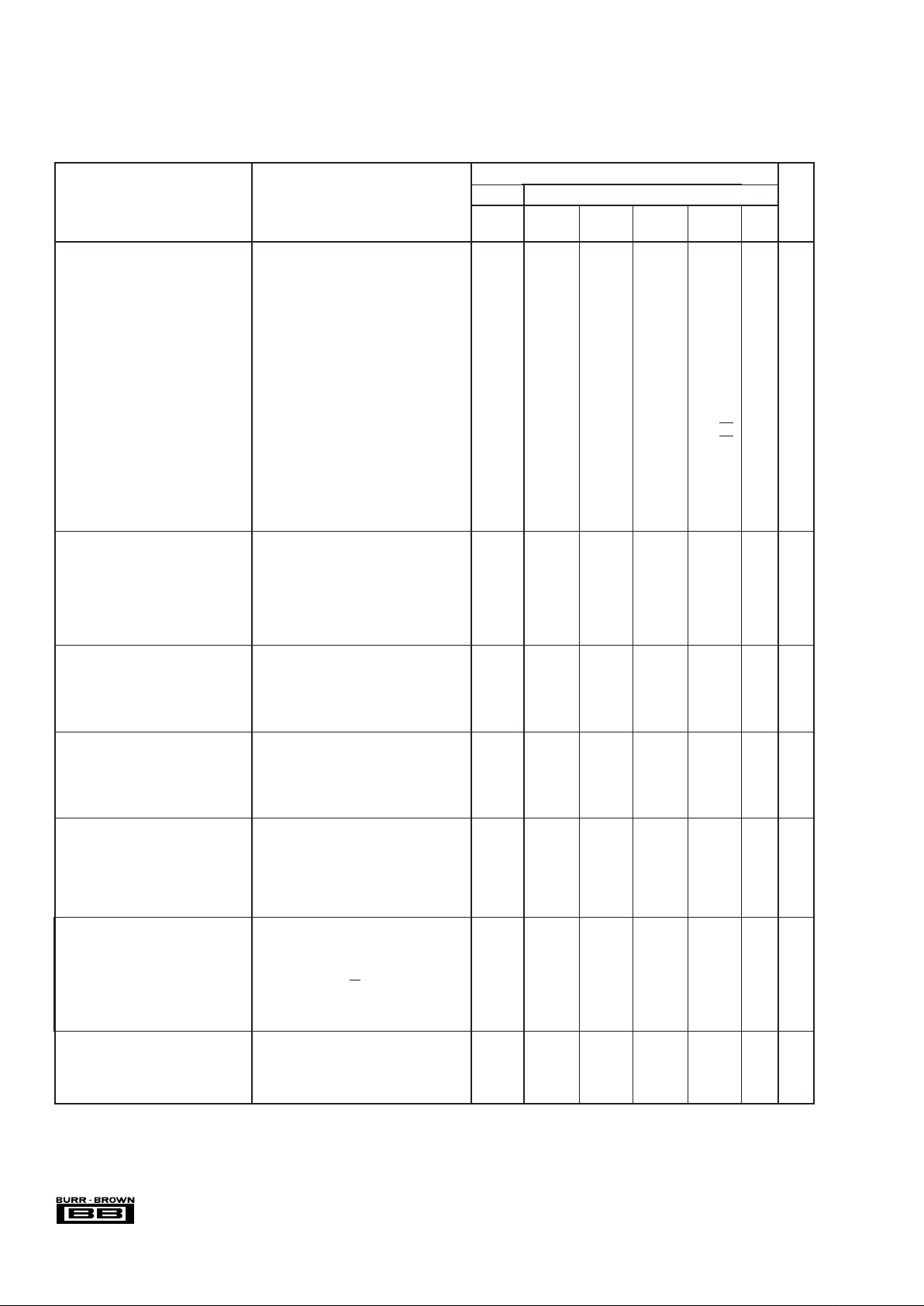
PIN CONFIGURATION
Top View SO-8
Top View SOT23-6
1
2
3
6
5
4
Output
–V
S
Noninverting Input
+V
S
DIS
Inverting Input
OPA687
123
654
A87
Pin Orientation/Package Marking
8
7
6
5
1
2
3
4
OPA687
NC: No Connection
NC
Inverting Input
Noninverting Input
–V
S
DIS
+V
S
Output
NC
4
®
OPA687
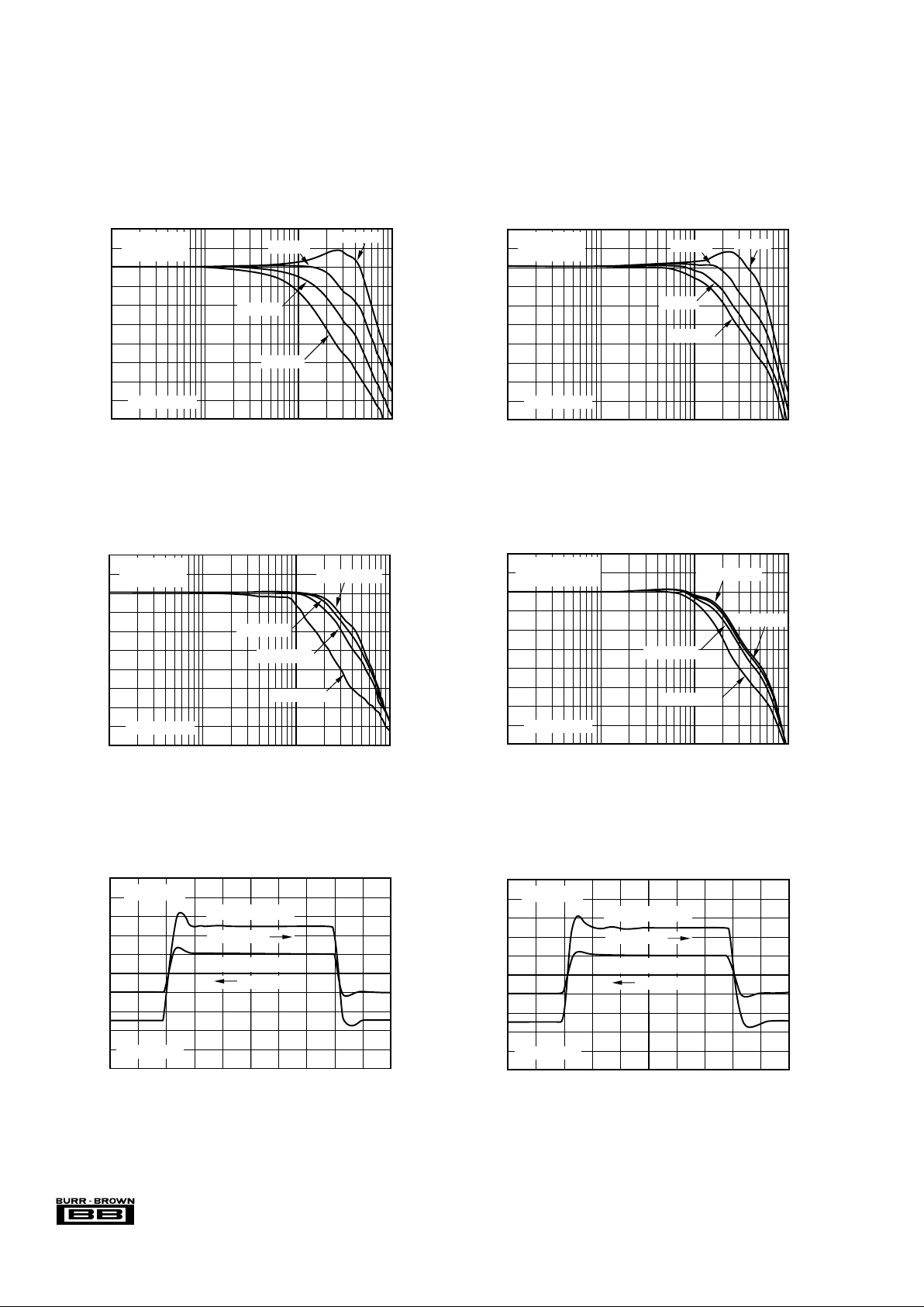
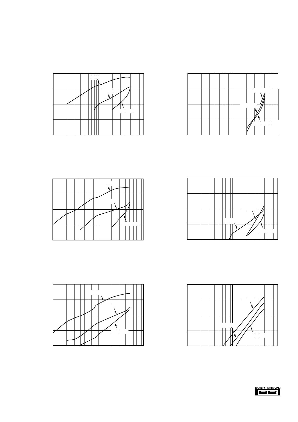
TYPICAL PERFORMANCE CURVES: VS = ±5V
RF = 750Ω, RG = 39.2Ω, G = +20 and RL = 100Ω, unless otherwise noted.
6
3
0
–3
–6
–9
–12
–15
–18
–21
–24
NONINVERTING SMALL-SIGNAL
FREQUENCY RESPONSE
Frequency (MHz)
Normalized Gain (3dB/div)
1 10 100 1000
RG = 39.2Ω
V
O
= 0.2Vp-p
G = +30
G = +50
See Figure 1
G = +12
G = +20
6
3
0
–3
–6
–9
–12
–15
–18
–21
–24
INVERTING SMALL-SIGNAL
FREQUENCY RESPONSE
Frequency (MHz)
Normalized Gain (3dB/div)
1 10 100 1000
RG = RS = 50Ω
V
O
= 0.2Vp-p
G = –40
G = –50
See Figure 2
G = –20
G = –30
32
29
26
23
20
17
14
11
8
5
2
NONINVERTING LARGE-SIGNAL
FREQUENCY RESPONSE
Frequency (MHz)
Gain (3dB/div)
1 10 100 1000
RG = 39.2Ω
G = +20V/V
VO = 2Vp-p
VO = 0.2Vp-p
VO = 5Vp-p
See Figure 1
VO = 1Vp-p
200
100
0
–100
–200
1.2
0.8
0.4
0
–0.4
–0.8
–1.2
NONINVERTING PULSE RESPONSE
Time (5ns/div)
Output Voltage (100mV/div)
Output Voltage (400mV/div)
G = +20V/V
See Figure 1
Large Signal ±1V
Small Signal ±100mV
Right Scale
Left Scale
38
35
32
29
26
23
20
18
14
13
10
INVERTING LARGE-SIGNAL
FREQUENCY RESPONSE
Frequency (MHz)
Gain (3dB/div)
1 10 100 1000
RG = RS = 50Ω
G = –40V/V
VO = 2Vp-p
VO = 0.2Vp-p
See Figure 2
VO = 1Vp-p
VO = 5Vp-p
200
100
0
–100
–200
1.2
0.8
0.4
0
–0.4
–0.8
–1.2
INVERTING PULSE RESPONSE
Time (5ns/div)
Output Voltage (100mV/div)
Output Voltage (400mV/div)
G = –40V/V
See Figure 2
Large Signal ±1V
Small Signal ±100mV
Right Scale
Left Scale
5
®
OPA687
TYPICAL PERFORMANCE CURVES: VS = ±5V (CONT)
RF = 750Ω, RG = 39.2Ω, G = +20 and RL = 100Ω, unless otherwise noted (Figure 1).
–70
–80
–90
–100
–110
Output Voltage (Vp-p)
0.1 101
5MHz 2nd HARMONIC DISTORTION
vs OUTPUT VOLTAGE
2nd Harmonic Distortion (dBc)
RL = 200Ω
RL = 100Ω
RL = 500Ω
–70
–80
–90
–100
–110
Output Voltage (Vp-p)
0.1 101
5MHz 3rd HARMONIC DISTORTION
vs OUTPUT VOLTAGE
3rd Harmonic Distortion (dBc)
RL = 100Ω
RL = 500Ω
RL =200Ω
–60
–70
–80
–90
–100
Output Voltage (Vp-p)
0.1 101
10MHz 2nd HARMONIC DISTORTION
vs OUTPUT VOLTAGE
2nd Harmonic Distortion (dBc)
RL = 200Ω
RL = 100Ω
RL = 500Ω
–60
–70
–80
–90
–100
Output Voltage (Vp-p)
0.1 101
10MHz 3rd HARMONIC DISTORTION
vs OUTPUT VOLTAGE
3rd Harmonic Distortion (dBc)
RL = 200Ω
RL = 100Ω
RL = 500Ω
–50
–60
–70
–80
–90
Output Voltage (Vp-p)
0.1 101
20MHz 2nd HARMONIC DISTORTION
vs OUTPUT VOLTAGE
2nd Harmonic Distortion (dBc)
RL = 200Ω
RL = 100Ω
RL = 500Ω
–50
–60
–70
–80
–90
Output Voltage (Vp-p)
0.1 101
20MHz 3rd HARMONIC DISTORTION
vs OUTPUT VOLTAGE
3rd Harmonic Distortion (dBc)
RL = 200Ω
RL = 100Ω
RL = 500Ω
 Loading...