

Burr Brown OPA686U-2K5, OPA686U, OPA686N-3K, OPA686N-250 Datasheet
1
®
OPA686
International Airport Industrial Park • Mailing Address: PO Box 11400, Tucson, AZ 85734 • Street Address: 6730 S. Tucson Blvd., Tucson, AZ 85706 • Tel: (520) 746-1111 • Twx: 910-952-1111
Internet: http://www.burr-brown.com/ • FAXLine: (800) 548-6133 (US/Canada Only) • Cable: BBRCORP • Telex: 066-6491 • FAX: (520) 889-1510 • Immediate Product Info: (800) 548-6132
OPA686
®
Wideband, Low Noise,
Voltage Feedback OPERATIONAL AMPLIFIER
APPLICATIONS
● HIGH DYNAMIC RANGE ADC PREAMP
● LOW NOISE, WIDEBAND,
TRANSIMPEDANCE AMPLIFIER
● WIDEBAND, HIGH GAIN AMPLIFIER
● LOW NOISE DIFFERENTIAL RECEIVER
● VDSL LINE RECEIVER
● ULTRASOUND CHANNEL AMPLIFIER
● IMPROVED REPLACEMENT FOR THE
CLC425
FEATURES
● HIGH BANDWIDTH: 250MHz (G = +10)
● LOW INPUT VOLTAGE NOISE: 1.3nV/√Hz
● VERY LOW DISTORTION: –90dBc (5MHz)
● HIGH SLEW RATE: 600V/µs
● HIGH DC ACCURACY
● LOW SUPPLY CURRENT: 12mA
● HIGH GAIN BANDWIDTH PRODUCT:
1600MHz
● STABLE FOR GAINS ≥ 7
DESCRIPTION
The OPA686 combines very high gain bandwidth and large
signal performance with very low input voltage noise while
dissipating a low 12mA supply current. The classical differential input stage, along with two stages of forward gain and a
high power output stage, combine to make the OPA686 an
exceptionally low distortion amplifier with excellent DC accuracy and output drive. The voltage feedback architecture allows
all standard op amp applications to be implemented with very
high performance.
The combination of low input voltage and current noise, along
with a 1.6GHz gain bandwidth product, make the OPA686 an
ideal amplifier for wideband transimpedance stages. As a voltage gain stage, the OPA686 is optimized for a flat response at a
gain of +10 and is guaranteed stable down to a noise gain of +7.
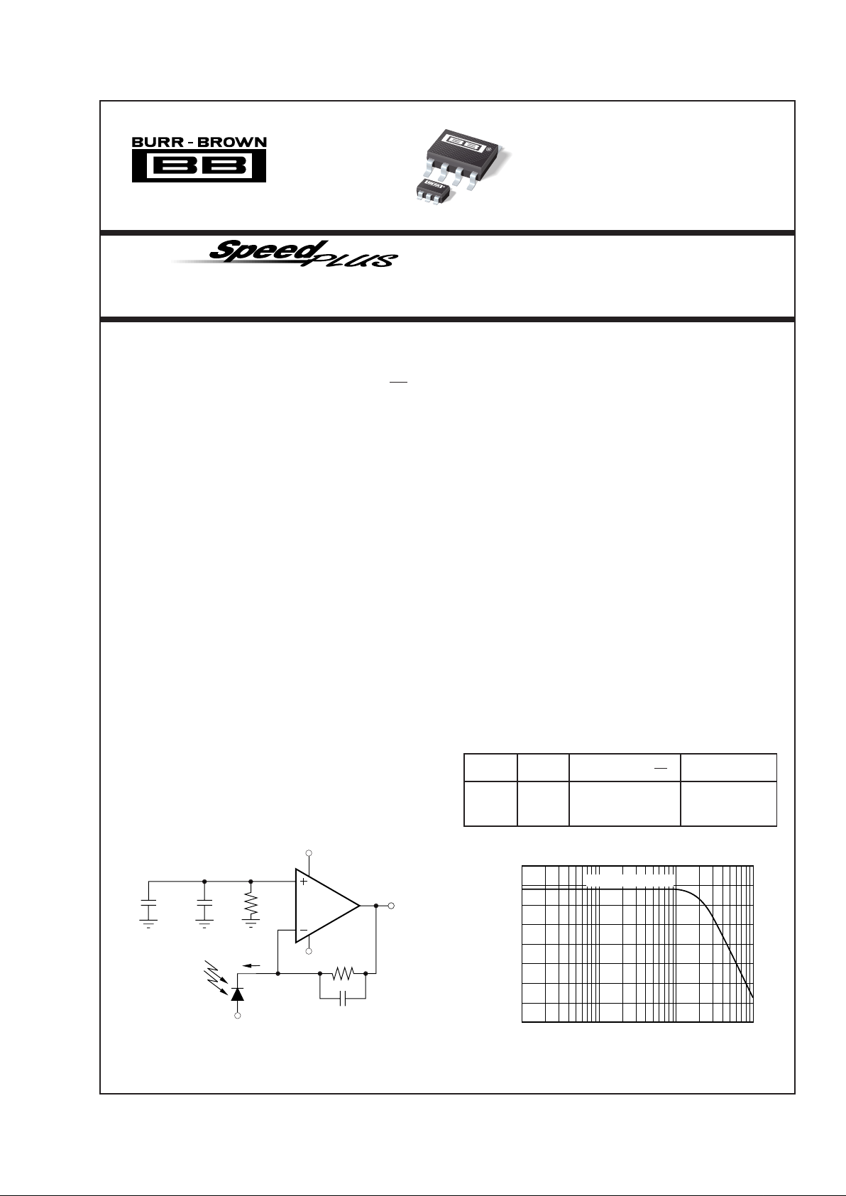
High Gain, 20MHz Transimpedance Amplifier
TM
A new external compensation technique can be used to give a
very flat frequency response below the minimum stable gain
for the OPA686, further improving its already exceptional
distortion performance. Using this compensation makes the
OPA686 one of the premier 12- to 14-bit analog-to-digital
converter input drivers. The supply current for the OPA686 is
precisely trimmed to 12.4mA at +25°C. This, along with
carefully defined supply current tempcos in the input and
output stages, combine to provide exceptional performance
over the full specified temperature range.
OPA686
OPA686
©
1997 Burr-Brown Corporation PDS-1370D Printed in U.S.A. May, 2000
OPA686
+5V
–5V
V
O
50kΩ
0.1µF100pF
50kΩ
0.2pF
10pF
Photodiode
I
S
–V
B
Supply decoupling
not shown.
λ
100
95
90
85
80
75
70
65
60
Frequency (MHz)
0.1 1 10 100
20•log (Z
T
) 5dB/div
20log (50kΩ) = 94dBΩ
OPA686 RELATED PRODUCTS
INPUT NOISE GAIN BANDWIDTH
SINGLES DUALS VOLTAGE (nV/
√Hz) PRODUCT (MHz)
OPA643 2.3 800
OPA2686 1.3 1600
OPA687 0.95 3600
For most current data sheet and other product
information, visit www.burr-brown.com
2
®
OPA686
OPA686U, N
TYP GUARANTEED
0°C to –40°C to
MIN/
TEST
PARAMETER CONDITIONS +25°C +25°C
(2)
70°C
(3)
+85°C
(3)
UNITS MAX
LEVEL
(1)
SPECIFICATIONS: VS = ±5V
RF = 453Ω, RL = 100Ω, and G =+10, unless otherwise noted. Figure 1 for AC performance.
AC PERFORMANCE (Figure 1)
Closed-Loop Bandwidth G = +7, R
G
= 50Ω, VO = 200mVp-p 425 MHz typ C
G = +10, R
G
= 50Ω, VO = 200mVp-p 250 200 170 140 MHz min B
G = +20, R
G
= 50Ω, VO = 200mVp-p 100 80 65 55 MHz min B
Gain Bandwidth Product G ≥ +40 1600 1250 1100 1000 MHz min B
Bandwidth for 0.1dB Gain Flatness G = +10, R
L
= 100Ω, VO = 200mVp-p 40 35 30 25 MHz min B
Peaking at a Gain of +7 2 dB typ C
Harmonic Distortion G = +10, f = 5MHz, V
O
= 2Vp-p
2nd Harmonic R
L
= 100Ω –72 –67 –65 –60 dBc max B
R
L
= 500Ω –90 –85 –80 –75 dBc max B
3rd Harmonic R
L
= 100Ω –95 –90 –85 –80 dBc max B
R
L
= 500Ω –110 –105 –100 –95 dBc max B
Two-Tone, 3rd-Order Intercept G = +10, f = 10MHz 43 40 39 37 dBm min B
Input Voltage Noise f > 1MHz 1.3 1.5 1.6 1.7 nV/√Hz max B
Input Current Noise f > 1MHz 1.8 2.3 2.4 2.5 pA/√Hz max B
Rise/Fall Time 0.2V Step 1.4 1.75 2 2.5 ns max B
Slew Rate 2V Step 600 500 400 310 V/µs min B
Settling Time to 0.01% 2V Step 18 ns typ C
0.1% 2V Step 16 14 21 25 ns max B
1% 2V Step 11 12 14 18 ns max B
Differential Gain G = +10, NTSC, R
L
= 150Ω 0.02 % typ C
Differential Phase G = +10, NTSC, R
L
= 150Ω 0.02 deg typ C
DC PERFORMANCE
(4)
Open-Loop Voltage Gain (AOL)V
O
= 0V 80 75 70 70 dB min A
Input Offset Voltage V
CM
= 0V ±0.35 ±1.0 ±1.2 ±1.5 mV max A
Average Offset Voltage Drift V
CM
= 0V 5 10 µV/°C max B
Input Bias Current V
CM
= 0V –10 –17 –18 –20 µA max A
Input Bias Current Drift V
CM
= 0V 50 100 nA/°C max B
Input Offset Current V
CM
= 0V ±0.5 ±1.0 ±1.5 ±1.8 µA max A
Input Offset Current Drift V
CM
= 0V 5 10 nA/°C max B
INPUT
Common-Mode Input Range (CMIR)
(5)
±3.2 ±3.0 ±2.9 ±2.8 V min A
Common-Mode Rejection (CMR) V
CM
= ±1V, Input Referred 100 90 85 75 dB min A
Input Impedance
Differential-Mode V
CM
= 0V 6 || 2 kΩ || pF typ C
Common-Mode V
CM
= 0V 2.9 || 1 MΩ || pF typ C
OUTPUT
Output Voltage Swing ≥ 400Ω Load ±3.5
±3.2 ±3.1 ±3.0 V min A
100Ω Load ±3.3
±3.0 ±2.8 ±2.8 V min A
Current Output, Sourcing V
O
= 0V 80 60 55 50 mA min A
Current Output, Sinking V
O
= 0V –80 –60 –55 –40 mA min A
Closed-Loop Output Impedance G = +10, f = 100kHz 0.008 Ω typ C
POWER SUPPLY
Specified Operating Voltage ±5 V typ C
Maximum Operating Voltage
±6 ±6 ±6 V max A
Max Quiescent Current V
S
= ±5V 12.4 12.9 13 13.9 mA max A
Min Quiescent Current V
S
= ±5V 12.4 11.9 11.9 11 mA min A
Power Supply Rejection Ratio
+PSRR, –PSRR |V
S
| = 4.5 to 5.5, Input Referred 78 70 70 65 dB min A
THERMAL CHARACTERISTICS
Specified Operating Range: U, N Package
–40 to +85
°C typ C
Thermal Resistance,
θ
JA
Junction-to-Ambient
U 8-Pin, SO-8 125 °C/W typ C
N 5-Pin, SOT23 150 °C/W typ C
NOTES: (1) Test Levels: (A) 100% tested at 25°C. Over temperature limits by characterization and simulation. (B) Limits set by characterization and simulation.
(C) Typical value only for information. (2) Junction temperature = ambient for 25°C guaranteed specifications. (3) Junction temperature = ambient at low temperature
limit: junction temperature = ambient +23°C at high temperature limit for over temperature guaranteed specifications. (4) Current is considered positive out-of-node.
V
CM
is the input common-mode voltage. (5) Tested < 3dB below minimum specified CMR at ±CMIR limits.
3
®
OPA686
The information provided herein is believed to be reliable; however, BURR-BROWN assumes no responsibility for inaccuracies or omissions. BURR-BROWN assumes
no responsibility for the use of this information, and all use of such information shall be entirely at the user’s own risk. Prices and specifications are subject to change
without notice. No patent rights or licenses to any of the circuits described herein are implied or granted to any third party. BURR-BROWN does not authorize or warrant
any BURR-BROWN product for use in life support devices and/or systems.
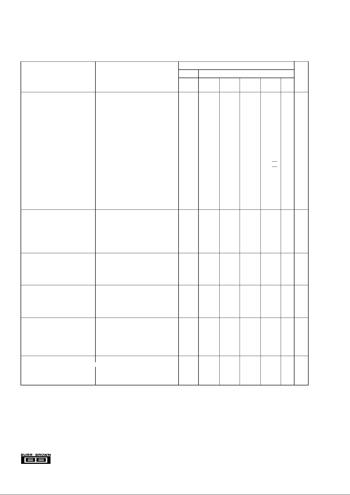
PIN CONFIGURATIONS
1
2
3
4
8
7
6
5
NC
Inverting Input
Non-Inverting Input
–V
S
DNC
+V
S
Output
NC
DNC: Do Not Connect
NC: No Connection
1
2
3
5
4
Output
–V
S
Non-Inverting Input
+V
S
Inverting Input
1
2
3
5
4
Pin Orientation/Package Marking
A86
Top View SOT23-5
Top View SO-8
PACKAGE
DRAWING TEMPERATURE PACKAGE ORDERING TRANSPORT
PRODUCT PACKAGE NUMBER
(1)
RANGE MARKING NUMBER
(2)
MEDIA
OPA686U SO-8 Surface Mount 182 –40°C to +85°C OPA686U OPA686U Rails
" """"OPA686U/2K5 Tape and Reel
OPA686N 5-Lead SOT23-5 331 –40°C to +85°C A86 OPA686N/250 Tape and Reel
" " " " OPA686N/3K Tape and Reel
NOTES: (1) For detailed drawing and dimension table, please see end of data sheet, or Appendix C of Burr-Brown IC Data Book. (2) Models with a slash (/ ) are
available only in Tape and Reel in the quantities indicated (e.g., /2K5 indicates 2500 devices per reel). Ordering 2500 pieces of “OPA686U/2K5” will get a single
2500-piece Tape and Reel. For detailed Tape and Reel mechanical information, refer to Appendix B of Burr-Brown IC Data Book.
PACKAGE/ORDERING INFORMATION
ABSOLUTE MAXIMUM RATINGS
Power Supply ............................................................................... ±6.5V
DC
Internal Power Dissipation ...................................... See Thermal Analysis
Differential Input Voltage .................................................................. ±1.2V
Input Voltage Range ............................................................................ ±V
S
Storage Temperature Range: U, N................................ –40°C to +125°C
Lead Temperature (soldering, 10s) .............................................. +300°C
Junction Temperature (T
J
) ........................................................... +175°C
ELECTROSTATIC
DISCHARGE SENSITIVITY
This integrated circuit can be damaged by ESD. Burr-Brown
recommends that all integrated circuits be handled with appropriate
precautions. Failure to observe proper handling and installation
procedures can cause damage.
ESD damage can range from subtle performance degradation to
complete device failure. Precision integrated circuits may be more
susceptible to damage because very small parametric changes
could cause the device not to meet its published specifications.
4
®
OPA686
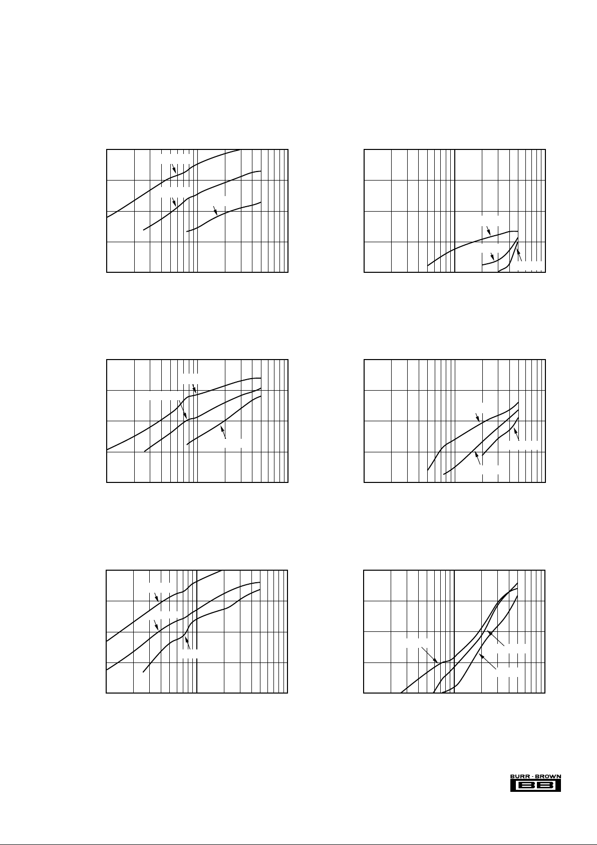
TYPICAL PERFORMANCE CURVES: VS = ±5V
At TA = +25°C, G = +10, RF = 453Ω, and RL = 100Ω, unless otherwise noted.
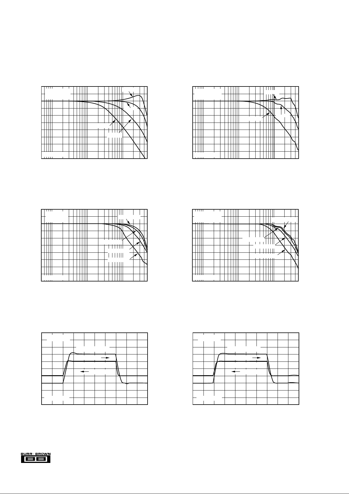
6
3
0
–3
–6
–9
–12
–15
–18
–21
–24
NON-INVERTING SMALL-SIGNAL
FREQUENCY RESPONSE
Frequency (MHz)
Normalized Gain (3dB/div)
0.5 10 100 500
G = +50
See Figure 1
RG = 50Ω
V
O
= 0.2Vp-p
G = +20
G = +7
G = +10
26
23
20
17
14
11
8
5
2
–1
–4
NON-INVERTING LARGE-SIGNAL
FREQUENCY RESPONSE
Frequency (MHz)
Gain (3dB/div)
0.5 10 100 500
RG = 50Ω
G = +10V/V
VO = 0.2Vp-p
VO = 1Vp-p
VO = 2Vp-p
V
O
= 5Vp-p
See Figure 1
30
29
26
23
20
17
14
11
8
5
2
INVERTING LARGE-SIGNAL FREQUENCY RESPONSE
Frequency (MHz)
Gain (3dB/div)
0.1 10 100 500
RG = RS = 50Ω
G = –20V/V
VO = 0.2Vp-p
VO = 1Vp-p
VO = 2Vp-p
V
O
= 5Vp-p
See Figure 2
100
0
–100
1.5
1.0
0.5
0
–0.5
–1.0
–1.5
NON-INVERTING PULSE RESPONSE
Time (5ns/div)
Output Voltage (100mV/div)
Output Voltage (500mV/div)
G = +10V/V
Large Signal ±1V
Small Signal ±100mV
Right Scale
Left Scale
See Figure 1
100
0
–100
1.5
1.0
0.5
0
–0.5
–1.0
–1.5
INVERTING PULSE RESPONSE
Time (5ns/div)
Output Voltage (100mV/div)
Output Voltage (500mV/div)
G = –20V/V
Large Signal ±1V
Small Signal ±100mV
Right Scale
Left Scale
See Figure 2
6
3
0
–3
–6
–9
–12
–15
–18
–21
–24
INVERTING SMALL-SIGNAL FREQUENCY RESPONSE
Frequency (MHz)
Normalized Gain (3dB/div)
0.5 10 100 500
RG = RS = 50Ω
V
O
= 0.2Vp-p
G = –12
G = –50
G = –20
See Figure 2
5
®
OPA686
TYPICAL PERFORMANCE CURVES: VS = ±5V (CONT)
At TA = +25°C, G = +10, RG = 50Ω, and RL = 100Ω, unless otherwise noted. See Figure 1.
–70
–80
–90
–100
–110
Output Voltage (Vp-p)
0.1 101
5MHz 2nd HARMONIC DISTORTION
vs OUTPUT VOLTAGE
2nd Harmonic Distortion (dBc)
RL = 200Ω
RL = 100Ω
RL = 500Ω
–70
–80
–90
–100
–110
Output Voltage (Vp-p)
0.1 101
5MHz 3rd HARMONIC DISTORTION
vs OUTPUT VOLTAGE
3rd Harmonic Distortion (dBc)
RL = 200Ω
RL = 100Ω
RL = 500Ω
–60
–70
–80
–90
–100
Output Voltage (Vp-p)
0.1 101
10MHz 2nd HARMONIC DISTORTION
vs OUTPUT VOLTAGE
2nd Harmonic Distortion (dBc)
RL = 200Ω
RL = 100Ω
RL = 500Ω
–60
–70
–80
–90
–100
Output Voltage (Vp-p)
0.1 101
10MHz 3rd HARMONIC DISTORTION
vs OUTPUT VOLTAGE
3rd Harmonic Distortion (dBc)
RL = 200Ω
RL = 500Ω
RL = 500Ω
–50
–60
–70
–80
–90
Output Voltage (Vp-p)
0.1 101
20MHz 2nd HARMONIC DISTORTION
vs OUTPUT VOLTAGE
2nd Harmonic Distortion (dBc)
RL = 200Ω
RL = 100Ω
RL = 500Ω
–50
–60
–70
–80
–90
20MHz 3rd HARMONIC DISTORTION
vs OUTPUT VOLTAGE
Output Voltage (Vp-p)
0.1 1 10
3rd Harmonic Distortion (dBc)
RL = 100Ω
RL = 200Ω
RL = 500Ω
 Loading...