

Burr Brown OPA681U, OPA681U-2K5, OPA681N-250, OPA681N-3K, OPA681P Datasheet
Wideband, Current Feedback
OPERATIONAL AMPLIFIER With Disable
TM
DESCRIPTION
The OPA681 sets a new level of performance for broadband
current feedback op amps. Operating on a very low 6mA
supply current, the OPA681 offers a slew rate and output
power normally associated with a much higher supply current. A new output stage architecture delivers a high output
current with minimal voltage headroom and crossover
distortion. This gives exceptional single-supply operation.
Using a single +5V supply, the OPA681 can deliver a 1V to
4V output swing with over 100mA drive current and 150MHz
bandwidth. This combination of features makes the OPA681
an ideal RGB line driver or single-supply ADC input driver.
The OPA681’s low 6mA supply current is precisely trimmed
at 25°C. This trim, along with low drift over temperature,
OPA681
®
FEATURES
●
WIDEBAND +5V OPERATION: 225MHz (G = +2)
●
UNITY GAIN STABLE: 280MHz (G = 1)
● HIGH OUTPUT CURRENT: 150mA
● OUTPUT VOLTAGE SWING: ±4.0V
● HIGH SLEW RATE: 2100V/µs
● LOW dG/dφ: .001%/.01°
● LOW SUPPLY CURRENT: 6mA
● LOW DISABLED CURRENT: 320µA
APPLICATIONS
● xDSL LINE DRIVER
● BROADBAND VIDEO BUFFERS
● HIGH SPEED IMAGING CHANNELS
● PORTABLE INSTRUMENTS
● ADC BUFFERS
● ACTIVE FILTERS
● WIDEBAND INVERTING SUMMING
● HIGH SFDR IF AMPLIFIER
guarantees lower guaranteed maximum supply current than
competing products. System power may be further reduced by
using the optional disable control pin. Leaving this disable pin
open, or holding it high, gives normal operation. If pulled low,
the OPA681 supply current drops to less than 320µA while the
output goes into a high impedance state. This feature may be
used for either power savings or for video MUX applications.
OPA681 RELATED PRODUCTS
SINGLES DUALS TRIPLES
Voltage Feedback OPA680 OPA2680 OPA3680
Current Feedback OPA681 OPA2681 OPA3681
Fixed Gain OPA682 OPA2682 OPA3682
OPA681
OPA681
O
P
A
6
8
1
©
1997 Burr-Brown Corporation PDS-1427C Printed in U.S.A. March, 1999
International Airport Industrial Park • Mailing Address: PO Box 11400, Tucson, AZ 85734 • Street Address: 6730 S. Tucson Blvd., Tucson, AZ 85706 • Tel: (520) 746-1111
Twx: 910-952-1111 • Internet: http://www.burr-brown.com/ • Cable: BBRCORP • Telex: 066-6491 • FAX: (520) 889-1510 • Immediate Product Info: (800) 548-6132
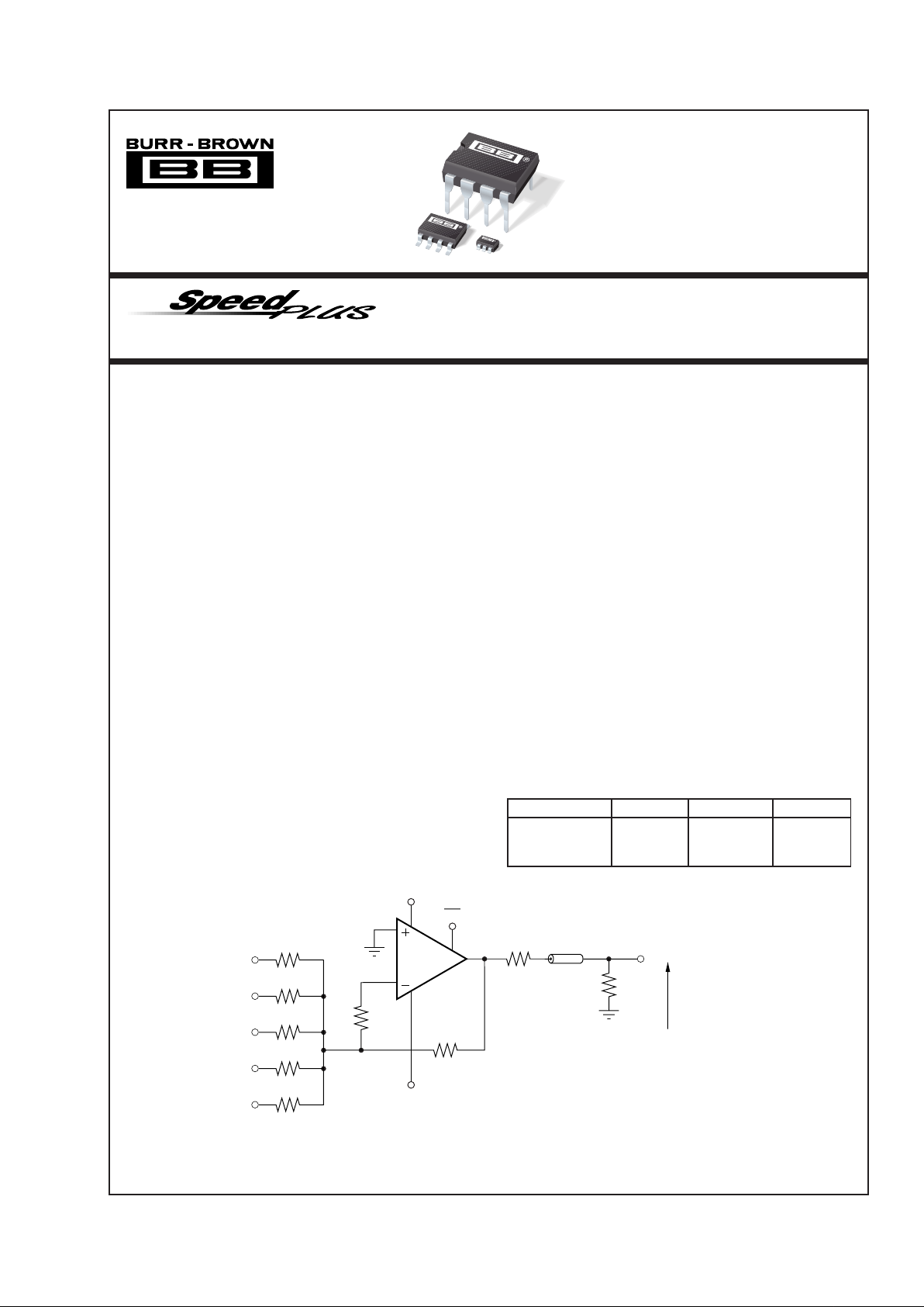
100Ω
50Ω
OPA681
+5V
DIS
–5V
VO = – (V1 + V2 + V3 + V4 + V5)
100MHz, –1dB Compression
= 15dBm
50Ω
V
2
50Ω
V
3
50Ω
V
4
50Ω
V
1
50Ω
RG-58
50Ω
V
5
23.7Ω
200MHz RF Summing Amplifier
2
®
OPA681
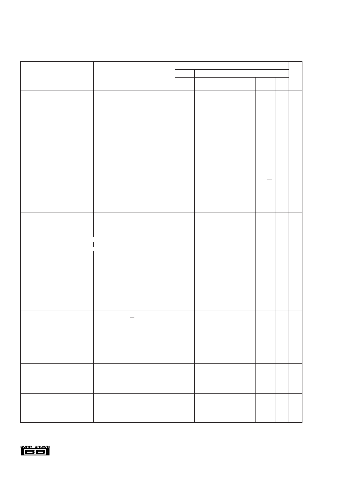
SPECIFICATIONS: VS = ±5V
RF = 402Ω, RL = 100Ω, and G = +2, (Figure 1 for AC performance only), unless otherwise noted.
OPA681P, U, N
TYP GUARANTEED
0°C to –40°C to
MIN/
TEST
PARAMETER CONDITIONS +25°C +25°C
(2)
70°C
(3)
+85°C
(3)
UNITS MAX
LEVEL
(1)
AC PERFORMANCE (Figure 1)
Small-Signal Bandwidth (VO = 0.5Vp-p) G = +1, RF = 453Ω 280 MHz typ C
G = +2, RF = 402Ω 220 220 210 190 MHz min B
G = +5, RF = 261Ω 185 MHz typ C
G = +10, RF = 180Ω 180 MHz typ C
Bandwidth for 0.1dB Gain Flatness G = +2, VO = 0.5Vp-p 90 50 45 45 MHz min B
Peaking at a Gain of +1 RF = 453, VO = 0.5Vp-p 0.4 2 4 dB max B
Large Signal Bandwidth G = +2, VO = 5Vp-p 150 MHz typ C
Slew Rate G = +2, 4V Step 2100 1600 1600 1200 V/µs min B
Rise/Fall Time G = +2, VO = 0.5V Step 1.7 ns typ C
G = +2, 5V Step 2.0 ns typ C
Settling Time to 0.02% G = +2, VO = 2V Step 12 ns typ C
0.1% G = +2, VO = 2V Step 8 ns typ C
Harmonic Distortion G = +2, f = 5MHz, V
O
= 2Vp-p
2nd Harmonic RL = 100Ω –79 –73 –70 –68 dBc max B
RL ≥ 500Ω –85 –77 –70 –69 dBc max B
3rd Harmonic RL = 100Ω –74 –71 –71 –68 dBc max B
RL ≥ 500Ω –77 –75 –74 –72 dBc max B
Input Voltage Noise f > 1MHz 2.5 3.0 3.4 3.6 nV/√Hz max B
Non-Inverting Input Current Noise f > 1MHz 12 14 15 15 pA/√Hz max B
Inverting Input Current Noise f > 1MHz 15 18 18 19 pA/√Hz max B
Differential Gain G = +2, NTSC, VO = 1.4Vp, RL = 150Ω 0.001 % typ C
RL = 37.5Ω 0.008 % typ C
Differential Phase G = +2, NTSC, VO = 1.4Vp, RL = 150Ω 0.01 deg typ C
RL = 37.5Ω 0.05 deg typ C
DC PERFORMANCE
(4)
Open-Loop Transimpedance Gain (ZOL)
VO = 0V, RL = 100Ω 100 56 56 56 kΩ min A
Input Offset Voltage VCM = 0V ±1.3 ±5 ±6.5 ±7.5 mV max A
Average Offset Voltage Drift VCM = 0V +35 +40 µV/°C max B
Non-Inverting Input Bias Current VCM = 0V +30 +55 ±65 ±85 µA max A
Average Non-Inverting Input Bias Current Drift VCM = 0V –400 –450 nA/°C max B
Inverting Input Bias Current VCM = 0V ±10 ±40 ±50 ±55 µA max A
Average Inverting Input Bias Current Drift VCM = 0V –125 –150 nA°/C max B
INPUT
Common-Mode Input Range
(5)
±3.5 ±3.4 ±3.3 ±3.2 V min A
Common-Mode Rejection VCM = 0V 52 47 46 45 dB min A
Non-Inverting Input Impedance 100 || 2 kΩ || pF typ C
Min Inverting Input Resistance (RI)
Open-Loop 41 33 31 30 Ω min A
Max Inverting Input Resistance (RI)
Open-Loop 41 48 50 55 Ω max A
OUTPUT™
Voltage Output Swing No Load ±4.0
±3.8 ±3.7 ±3.6 V min A
100Ω Load ±3.9 ±3.7 ±3.6 ±3.3 V min A
Current Output, Sourcing VO = 0 +190 +160 +140 +80 mA min A
Current Output, Sinking VO = 0 –150 –135 –130 –80 mA min A
Closed-Loop Output Impedance G = +2, f = 100kHz 0.03 Ω typ C
DISABLE (Disabled Low)
Power Down Supply Current (+V
S
)V
DIS
= 0 –320 µA typ C
Disable Time 100 ns typ C
Enable Time 25 ns typ C
Off Isolation G = +2, 5MHz 70 dB typ C
Output Capacitance in Disable 4 pF typ C
Turn On Glitch G = +2, RL = 150Ω, VIN = 0 ±50 mV typ C
Turn Off Glitch G = +2, RL = 150Ω, VIN = 0 ±20 mV typ C
Enable Voltage 3.3 3.5 3.6 3.7 V min A
Disable Voltage 1.8 1.7 1.6 1.5 V max A
Control Pin Input Bias Current (DIS) V
DIS
= 0 100 160 160 160 µA max A
POWER SUPPLY
Specified Operating Voltage ±5 V typ C
Maximum Operating Voltage Range
±6 ±6 ±6 V max A
Max Quiescent Current VS = ±5V 6 6.4 6.5 6.6 mA max A
Min Quiescent Current VS = ±5V 6 5.6 5.5 5.0 mA min A
Power Supply Rejection Ratio (–PSRR) Input Referred 58 52 50 49 dB min A
TEMPERATURE RANGE
Specification: P, U, N
–40 to +85
°C typ C
Thermal Resistance,
θ
JA
Junction-to-Ambient
P 8-Pin DIP 100 °C/W typ C
U SO-8 125 °C/W typ C
N SOT23-6 150 °C/W typ C
NOTES: (1) Test levels: (A) 100% tested at 25°C. Over temperature limits by characterization and simulation. (B) Limits set by characterization and simulation.
(C) Typical value only for information. (2) Junction temperature = ambient for 25°C guaranteed specifications. (3) Junction temperature = ambient at low temperature
limit: junction temperature = ambient +23°C at high temperature limit for over temperature guaranteed specifications. (4) Current is considered positive out-of-node.
V
CM
is the input common-mode voltage. (5) Tested < 3dB below minimum specified CMR at ± CMIR limits.
®
OPA681
3
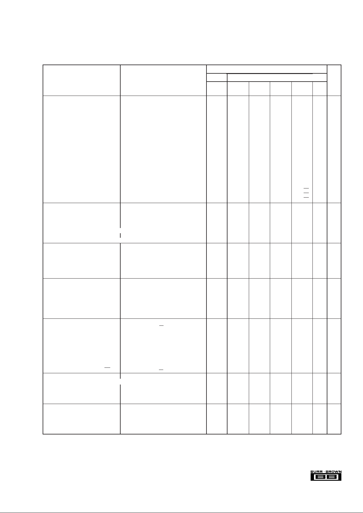
SPECIFICATIONS: VS = +5V
RF = 499Ω, RL = 100Ω to VS/ 2, and G = +2, (Figure 2 for AC performance only), unless otherwise noted.
OPA681P, U, N
TYP GUARANTEED
0°C to –40°C to
MIN/
TEST
PARAMETER CONDITIONS +25°C +25°C
(2)
70°C
(3)
+85°C
(3)
UNITS MAX
LEVEL
(1)
AC PERFORMANCE (Figure 2)
Small-Signal Bandwidth (VO = 0.5Vp-p) G = +1, RF = 649Ω 250 MHz typ C
G = +2, R
F
= 499Ω 225 180 140 110 MHz min B
G = +5, R
F
= 360Ω 180 MHz typ C
G = +10, R
F
= 200Ω 165 MHz typ C
Bandwidth for 0.1dB Gain Flatness G = +2, V
O
< 0.5Vp-p 100 50 35 23 MHz min B
Peaking at a Gain of +1 R
F
= 649Ω, VO < 0.5Vp-p 0.4 2 4 dB max B
Large-Signal Bandwidth G = +2, VO = 2Vp-p 200 MHz typ C
Slew Rate G = +2, 2V Step 830 700 680 570 V/µs min B
Rise/Fall Time G = +2, V
O
= 0.5V Step 1.5 ns typ C
G = +2, VO = 2V Step 2.0 ns typ C
Settling Time to 0.02% G = +2, V
O
= 2V Step 14 ns typ C
0.1% G = +2, V
O
= 2V Step 9 ns typ C
Harmonic Distortion G = +2, f = 5MHz, V
O
= 2Vp-p
2nd Harmonic RL = 100Ω to VS/2 –70 –68 –67 –63 dBc max B
RL ≥ 500Ω to VS/2 –72 –70 –70 –68 dBc max B
3rd Harmonic RL = 100Ω to VS/2 –72 –65 –65 –62 dBc max B
RL ≥ 500Ω to VS/2 –73 –68 –67 –67 dBc max B
Input Voltage Noise f > 1MHz 2.2 3 3.4 3.6 nV/√Hz max B
Non-Inverting Input Current Noise f > 1MHz 12 14 14 15 pA/√Hz max B
Inverting Input Current Noise f > 1MHz 15 18 18 19 pA/√Hz max B
DC PERFORMANCE
(4)
Open-Loop Transimpedance Gain (ZOL)
VO = VS/2, RL = 100Ω to VS/2 100 60 53 51 kΩ min A
Input Offset Voltage V
CM
= 2.5V ±1 ±5 ±6.0 ±7 mV max A
Average Offset Voltage Drift V
CM
= 2.5V +15 +20 µV/°C max B
Non-Inverting Input Bias Current V
CM
= 2.5V +40 +65 +75 +95 µA max A
Average Non-Inverting Input Bias Current Drift V
CM
= 2.5V –300 –350 nA/°C max B
Inverting Input Bias Current V
CM
= 2.5V ±5 ±20 ±25 ±35 µA max A
Average Inverting Input Bias Current Drift VCM = 2.5V –125 –175 nA/°C max B
INPUT
Least Positive Input Voltage
(5)
1.5 1.6 1.7 1.8 V max A
Most Positive Input Voltage
(5)
3.5 3.4 3.3 3.2 V min A
Common-Mode Rejection Ratio (CMRR)
VCM = VS/2 51 45 44 44 dB min A
Non-Inverting Input Impedance 100 || 2 kΩ || pF typ C
Min Inverting Input Resistance (RI)
Open-Loop 46 38 36 35 Ω min A
Max Inverting Input Resistance (RI)
Open-Loop 46 53 55 60 Ω max A
OUTPUT
Most Positive Output Voltage No Load 4 3.8 3.7 3.5 V min A
R
L
= 100Ω to VS/2 3.9 3.7 3.6 3.4 V min A
Least Positive Output Voltage No Load 1 1.2 1.3 1.5 V max A
R
L
= 100Ω to VS/2 1.1 1.3 1.4 1.6 V max A
Current Output, Sourcing V
O
= VS/2 150 110 110 60 mA min A
Current Output, Sinking V
O
= VS/2 –110 –75 –70 –50 mA min A
Closed-Loop Output Impedance G = +2, f = 100kHz 0.03 Ω typ C
DISABLE (Disable Low)
Power Down Supply Current (+V
S
)V
DIS
= 0 –270 µA typ C
Disable Time 100 ns typ C
Enable Time 25 ns typ C
Off Isolation G = +2, 5MHz 65 dB typ C
Output Capacitance in Disable 4 pF typ C
Turn On Glitch G = +2, R
L
= 150Ω, VIN = VS /2 ±50 mV typ C
Turn Off Glitch G = +2, R
L
= 150Ω, VIN = VS /2 ±20 mV typ C
Enable Voltage 3.3 3.5 3.6 3.7 V min A
Disable Voltage 1.8 1.7 1.6 1.5 V max A
Control Pin Input Bias Current (DIS) V
DIS
= 0 100 µA typ C
POWER SUPPLY
Specified Single-Supply Operating Voltage 5 V typ C
Max Single-Supply Operating Voltage 12 12 12 V max A
Max Quiescent Current V
S
= +5V 10.0 5.3 5.4 5.4 mA max A
Min Quiescent Current V
S
= +5V 10.0 4.1 3.7 3.6 mA min A
Power Supply Rejection Ratio (–PSRR) Input Referred 48 dB typ C
TEMPERATURE RANGE
Specification: P, U, N
–40 to +85
°C typ C
Thermal Resistance,
θ
JA
Junction-to-Ambient
P 8-Pin DIP 100 °C/W typ C
U SO-8 125 °C/W typ C
N SOT23-6 150 °C/W typ C
NOTES: (1) Test levels: (A) 100% tested at 25°C. Over temperature limits by characterization and simulation. (B) Limits set by characterization and simulation.
(C) Typical value only for information. (2) Junction temperature = ambient for 25°C guaranteed specifications. (3) Junction temperature = ambient at low temperature
limit: junction temperature = ambient +23°C at high temperature limit for over temperature guaranteed specifications. (4) Current is considered positive out-of-node.
V
CM
is the input common-mode voltage. (5) Tested < 3dB below minimum specified CMR at ±CMIR limits.
4
®
OPA681
ABSOLUTE MAXIMUM RATINGS
Power Supply .............................................................................. ±6.5VDC
Internal Power Dissipation
(1)
............................ See Thermal Information
Differential Input Voltage ..................................................................±1.2V
Input Voltage Range ............................................................................ ±V
S
Storage Temperature Range: P, U, N ........................... –40°C to +125°C
Lead Temperature (soldering, 10s) .............................................. +300°C
Junction Temperature (T
J
) ........................................................... +175°C
NOTE:: (1) Packages must be derated based on specified
θ
JA
. Maximum T
J
must be observed.
The information provided herein is believed to be reliable; however, BURR-BROWN assumes no responsibility for inaccuracies or omissions. BURR-BROWN assumes
no responsibility for the use of this information, and all use of such information shall be entirely at the user’s own risk. Prices and specifications are subject to change
without notice. No patent rights or licenses to any of the circuits described herein are implied or granted to any third party. BURR-BROWN does not authorize or warrant
any BURR-BROWN product for use in life support devices and/or systems.
PACKAGE SPECIFIED
DRAWING TEMPERATURE PACKAGE ORDERING TRANSPORT
PRODUCT PACKAGE NUMBER
(1)
RANGE MARKING NUMBER MEDIA
OPA681P 8-Pin Plastic DIP 006 –40°C to +85°C OPA681P OPA681P Rails
OPA681U SO-8 Surface Mount 182 –40°C to +85°C OPA681U OPA681U Rails
" " " " " OPA681U/2K5 Tape and Reel
OPA681N 6-Lead SOT23-6 332 –40°C to +85°C A81 OPA681N/250 Tape and Reel
" " " " " OPA681N/3K Tape and Reel
NOTES: (1) For detailed drawing and dimension table, please see end of data sheet, or Appendix C of Burr-Brown IC Data Book. (2) Models with a slash (/) are available
only as Tape and Reel in the quantity indicated after the slash (e.g. /2K5 indicates 2500 devices per reel). Ordering 3000 pieces of the OPA681N/3K will get a single
3000-piece Tape and Reel. For detailed Tape and Reel mechanical information, refer to Appendix B of the Burr-Brown IC Data Book.
PACKAGE/ORDERING INFORMATION
ELECTROSTATIC
DISCHARGE SENSITIVITY
Electrostatic discharge can cause damage ranging from performance degradation to complete device failure. Burr-Brown Corporation recommends that all integrated circuits be handled and stored
using appropriate ESD protection methods.
ESD damage can range from subtle performance degradation to
complete device failure. Precision integrated circuits may be more
susceptible to damage because very small parametric changes
could cause the device not to meet published specifications.
1
2
3
4
8
7
6
5
NC
Inverting Input
Non-Inverting Input
–V
S
DIS
+V
S
Output
NC
1
2
3
6
5
4
Output
–V
S
Non-Inverting Input
+V
S
DIS
Inverting Input
123
654
A81
Pin Orientation/Package Marking
PIN CONFIGURATION
Top View DIP/SO-8
NC = No Connection
Top View SOT23-6
®
OPA681
5
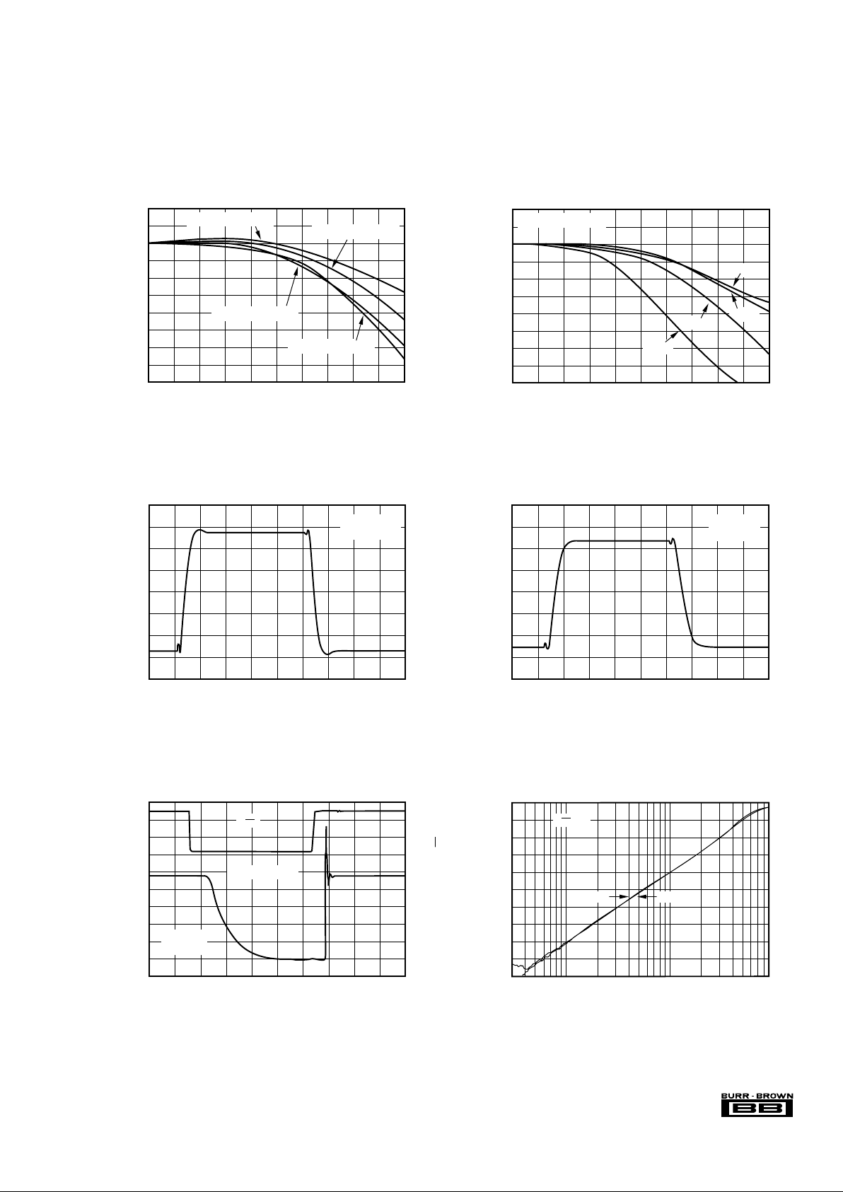
TYPICAL PERFORMANCE CURVES: VS = ±5V
G = +2, RF = 402Ω, and RL = 100Ω, unless otherwise noted (see Figure 1).
+4
+3
+2
+1
0
–1
–2
–3
–4
LARGE-SIGNAL PULSE RESPONSE
Time (5ns/div)
Output Voltage (1V/div)
G = +2
V
O
= 5Vp-p
400
300
200
100
0
–100
–200
–300
–400
SMALL-SIGNAL PULSE RESPONSE
Time (5ns/div)
Output Voltage (100mV/div)
G = +2
V
O
= 0.5Vp-p
DISABLED FEEDTHROUGH vs FREQUENCY
–45
–50
–55
–60
–65
–70
–75
–80
–85
–90
–95
Frequency (MHz)
1 10 100
Feedthrough (5dB/div)
Forward
V
DIS
= 0
Reverse
8
7
6
5
4
3
2
1
0
–1
–2
Frequency (25MHz/div)
0 250MHz125MHz
LARGE-SIGNAL FREQUENCY RESPONSE
Gain (1dB/div)
2Vp-p
G = +2, RL = 100Ω
1Vp-p
4Vp-p
7Vp-p
2.0
1.6
1.2
0.8
0.4
0
LARGE-SIGNAL DISABLE/ENABLE RESPONSE
Time (50ns/div)
Output Voltage (400mV/div)
6.0
4.0
2.0
0
V
DIS
(2V/div)
V
DIS
Output Voltage
G = +2
V
IN
= +1V
2
1
0
–1
–2
–3
–4
–5
–6
–7
–8
Frequency (25MHz/div)
0 250MHz125MHz
SMALL-SIGNAL FREQUENCY RESPONSE
Normalized Gain (1dB/div)
G = +10, RF = 180Ω
G = +5, RF = 261Ω
G = +1, RF = 453Ω
G = +2, RF = 402Ω
6
®
OPA681
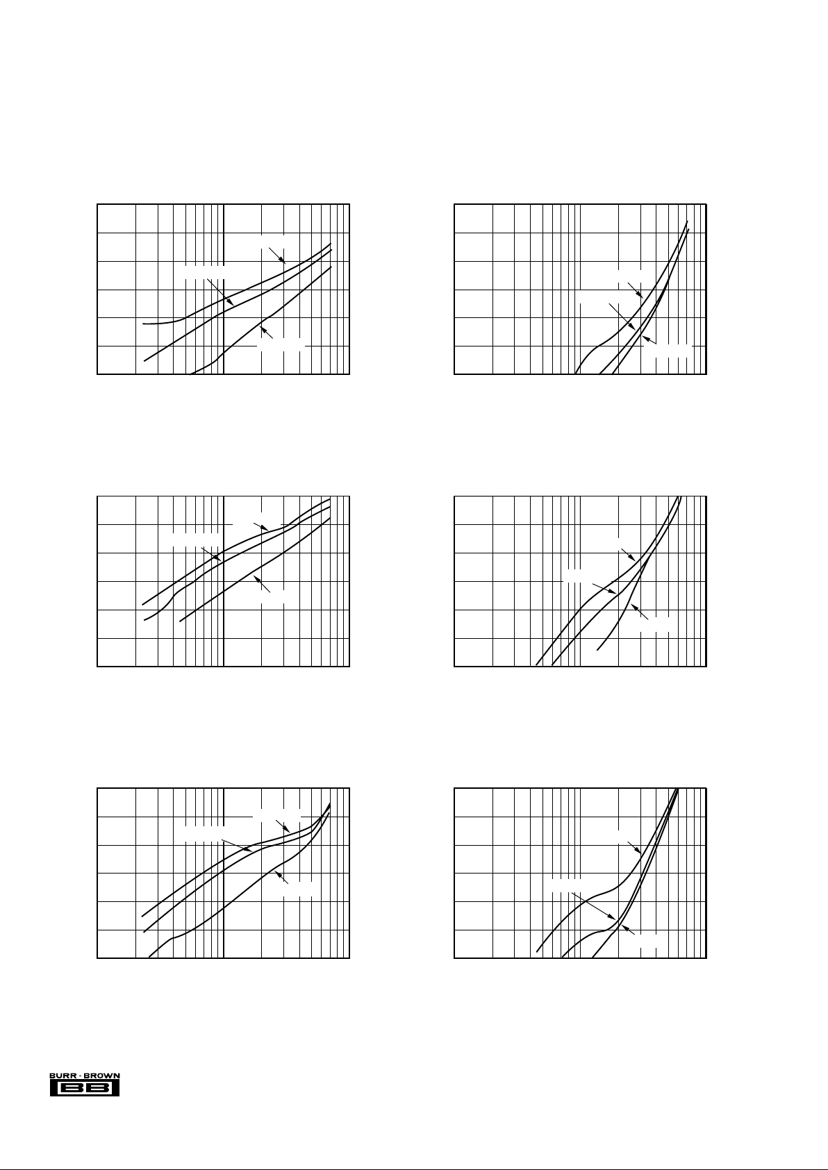
TYPICAL PERFORMANCE CURVES: VS = ±5V (CONT)
G = +2, RF = 402Ω, and RL = 100Ω, unless otherwise noted (see Figure 1).
–60
–65
–70
–75
–80
–85
–90
5MHz 2ND HARMONIC DISTORTION
vs OUTPUT VOLTAGE
Output Voltage Swing (Vp-p)
0.1 1 10
2nd Harmonic Distortion (dBc)
RL = 200Ω
RL = 500Ω
RL = 100Ω
–60
–65
–70
–75
–80
–85
–90
5MHz 3RD HARMONIC DISTORTION
vs OUTPUT VOLTAGE
Output Voltage Swing (Vp-p)
0.1 1 10
3rd Harmonic Distortion (dBc)
RL = 200Ω
RL = 100Ω
RL = 500Ω
–60
–65
–70
–75
–80
–85
–90
10MHz 2ND HARMONIC DISTORTION
vs OUTPUT VOLTAGE
Output Voltage Swing (Vp-p)
0.1 1 10
2nd Harmonic Distortion (dBc)
RL = 500Ω
RL = 100Ω
RL = 200Ω
–60
–65
–70
–75
–80
–85
–90
10MHz 3RD HARMONIC DISTORTION
vs OUTPUT VOLTAGE
Output Voltage Swing (Vp-p)
0.1 1 10
3rd Harmonic Distortion (dBc)
RL = 500Ω
RL = 100Ω
RL = 200Ω
–50
–55
–60
–65
–70
–75
–80
20MHz 2ND HARMONIC DISTORTION
vs OUTPUT VOLTAGE
Output Voltage Swing (Vp-p)
0.1 1 10
2nd Harmonic Distortion (dBc)
RL = 500Ω
RL = 100Ω
RL = 200Ω
–50
–55
–60
–65
–70
–75
–80
20MHz 3RD HARMONIC DISTORTION
vs OUTPUT VOLTAGE
Output Voltage Swing (Vp-p)
0.1 1 10
3rd Harmonic Distortion (dBc)
RL = 500Ω
RL = 100Ω
RL = 200Ω
®
OPA681
7
TYPICAL PERFORMANCE CURVES: VS = ±5V (CONT)
G = +2, RF = 402Ω, and RL = 100Ω, unless otherwise noted (see Figure 1).
–40
–50
–60
–70
–80
–90
2ND HARMONIC DISTORTION vs FREQUENCY
Frequency (MHz)
0.1 1 10 20
2nd Harmonic Distortion (dBc)
VO = 2Vp-p
R
L
= 100Ω
G = +2, RF = 402Ω
G = +10, RF = 180Ω
G = +5, RF = 261Ω
–40
–50
–60
–70
–80
–90
3RD HARMONIC DISTORTION vs FREQUENCY
Frequency (MHz)
0.1 1 10 20
3rd Harmonic Distortion (dBc)
VO = 2Vp-p
R
L
= 100Ω
G = +2,
R
F
= 402Ω
G = +10, RF = 180Ω
G = +5, RF = 261Ω
–40
–45
–50
–55
–60
–65
–70
–75
–80
–85
–90
TWO-TONE, 3RD-ORDER
INTERMODULATION SPURIOUS
Single-Tone Load Power (dBm)
–8–6–4–20246810
3rd-Order Spurious Level (dBc)
dBc = dB below carriers
50MHz
20MHz
10MHz
Load Power at Matched 50Ω Load
60
50
40
30
20
10
0
RECOMMENDED R
S
vs CAPACITIVE LOAD
Capacitive Load (pF)
1 10 100
R
S
(Ω)
15
12
9
6
3
0
–3
–6
–9
–12
–15
Frequency (30MHz/div)
0 300MHz150MHz
FREQUENCY RESPONSE vs CAPACITIVE LOAD
Gain to Capacitive Load (3dB/div)
OPA681
R
S
V
IN
V
O
C
L
1kΩ
402Ω
402Ω
1kΩ is optional.
CL = 22pF
CL = 10pF
CL = 47pF
CL = 100pF
100
10
1
INPUT VOLTAGE AND CURRENT NOISE DENSITY
Frequency (Hz)
100 1k 10k 100k 1M 10M
Current Noise (pA/√Hz)
Voltage Noise (nV/√Hz)
Non-Inverting Input Current Noise
Inverting Input Current Noise
12.2pA/√Hz
15.1pA/√Hz
Voltage Noise
2.2nV/√Hz
 Loading...