

Burr Brown OPA678AU Datasheet
®
OPA678
OPA678
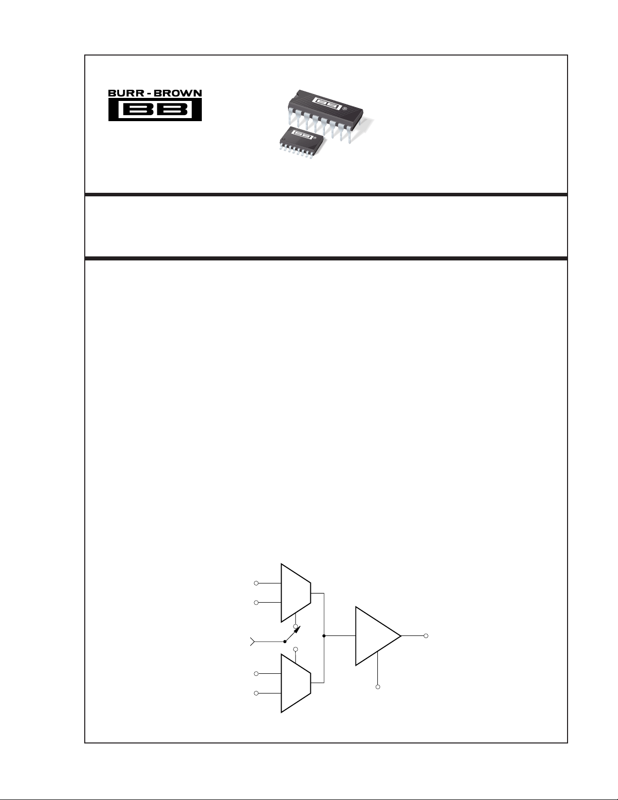
Wideband Switched-Input
OPERATIONAL AMPLIFIER
OPA678
FEATURES
● FAST SETTLING: 11ns (1%)
● WIDE BANDWIDTH: 200MHz
● TWO LOGIC SELECTABLE INPUTS
● LOW OFFSET VOLTAGE:
±380µV
● FAST INPUT SWITCHING: 4ns
● ACCEPTS TTL/ECL SWITCHING SIGNALS
● UNITY GAIN STABLE
● 16-PIN DIP AND SO-16 PACKAGES
DESCRIPTION
The OPA678 is a wideband monolithic operational
amplifier with two independent differential inputs.
Either input can be selected by an external TTL or
ECL logic signal. The amplifier is externally compensated and features a very fast input selection speed, 4ns
for either ECL or TTL. This amplifier features fully
symmetrical differential inputs due to its “classical”
APPLICATIONS
● VIDEO AMPLIFICATION AND SWITCHING
● FAST 2-INPUT MULTIPLEXER
● PULSE/RF AMPLIFIERS
● PROGRAMMABLE-GAIN AMPLIFIER
● ACTIVE FILTERS
● SYNCHRONOUS DEMODULATOR
● LOW COST REPLACEMENT FOR OPA675/676
operational amplifier circuit architecture. Unlike “current-feedback” amplifier designs, the OPA678 may be
used in all op amp applications requiring high speed
and precision.
Low distortion and crosstalk make this amplifier suitable for RF and video applications.
The OPA678 is available in plastic DIP and SO-16
packages.
Input A
A/B Channel
Select Input
(TTL or ECL)
Input B
International Airport Industrial Park • Mailing Address: PO Box 11400, Tucson, AZ 85734 • Street Address: 6730 S. Tucson Blvd., Tucson, AZ 85706 • Tel: (520) 746-1111 • Twx: 910-952-1111
Internet: http://www.burr-brown.com/ • FAXLine: (800) 548-6133 (US/Canada Only) • Cable: BBRCORP • Telex: 066-6491 • FAX: (520) 889-1510 • Immediate Product Info: (800) 548-6132
©
1992 Burr-Brown Corporation PDS-1136E Printed in U.S.A. March, 1998
–
+
–
+
A
B
Enable
A
Enable
B
Output
Compensation
®
1
OPA678
SPECIFICATIONS
ELECTRICAL
At VCC = ±5VDC, RL = 150Ω, C
PARAMETER CONDITIONS MIN TYP MAX UNITS
INPUT NOISE
(1)
Voltage: fO = 100Hz RS = 0Ω 55 nV/√Hz
f
= 1kHz 21 nV/√Hz
O
f
= 10kHz 7.8 nV/√Hz
O
f
= 100kHz 4.9 nV/√Hz
O
f
= 10Hz to 10MHz 18 µVrms
Current: f
OFFSET VOLTAGE
B
= 10Hz to 1MHz 2.1 pA/√Hz
O
(1)
Input Offset Voltage VCM = 0VDC ±380 ±1.5mV µV
Offset Voltage Drift T
Supply Rejection ±V
BIAS CURRENT
(1)
Input Bias Current VCM = 0VDC 14 50 µA
OFFSET CURRENT
(1)
Input Offset Current VCM = 0VDC 0.2 2 µA
INPUT IMPEDANCE
(1)
Differential 25k 2 Ω pF
Common-Mode 10
INPUT VOLTAGE RANGE
Common-Mode Input Range 2.0 ±2.5 V
Common-Mode Rejection V
OPEN-LOOP GAIN, DC
(1)
Open-Loop Voltage Gain 50 60 dB
FREQUENCY RESPONSE
Closed-Loop Bandwidth Gain = +1V/V, C
Crosstalk Gain = +1V/V, f = 100kHz –102 dBC
Harmonic Distortion: 5MHz G = +1V/V, R
Large Signal Response
(4)
Slew Rate Gain = +1V/V 250 350 V/µs
Settling Time: 1% Gain = –1V/V, 1V
0.1% 22 ns
0.01% 30 ns
Differential Gain (0V to 0.7V) 4.5MHz, Gain = +2V/V, C
Differential Phase (0V to 0.7V) 4.5MHz, Gain = +2V/V, C
INPUT SELECTION
(5)
Transition Time ECL: Operation 4 8 ns
50% In to 50% Out TTL: Operation 4 8 ns
DIGITAL INPUT
TTL Logic Levels: V
ECL Logic Levels:V
IL
V
IH
I
IL
I
IH
IL
V
IH
I
IL
I
IH
RATED OUTPUT
Voltage Output R
Current Output ±30 ±44 mA
Output Resistance 1MHz, Open-Loop, C
Load Capacitance Stability R
Short Circuit Current Continuous to Gnd +45 mA
= 5pF, and TA = +25°C, unless otherwise noted.
COMP
= T
A
= 4.5V to 5.5V 65 71 dB
CC
(1)
= ±0.5VDC, VO = ±1.25V 75 85 dB
IN
Gain = +2V/V, C
Gain = +5V/V, C
L
Second Harmonic –71 dBC
Third Harmonic –82 dBC
VO = 2.5Vp-p, Gain = +1V/V 32 45 MHz
Logic “LO” 0 +0.8 V
Logic “HI” +2.0 +5 V
Logic “LO”, VIL = 0V –0.05 –0.2 mA
Logic “HI”, VIH = +2.7V 1 20 µA
Logic “LO” –1.81 –1.475 V
Logic “HI” –1.15 – 0.88 V
Logic “LO”, VIL = –1.6V –50 –100 µA
Logic “HI”, VIH = –1.0V –50 –100 µA
R
= 100Ω, Gain = +1V/V, CC = 10pF 17 pF
F
OPA678AP, AU
to T
MIN
MAX
= 9pF 140 200 MHz
C
= 7pF 100 MHz
C
= 1pF 70 MHz
C
±3 ±15 µV/°C
6
5 Ω pF
f = 1MHz –83 dBC
f = 10MHz –64 dBC
f = 100MHz –44 dBC
= 150Ω, VO = 0.25Vp-p
Step 11 ns
OUT
= 2.2pF 0.02 %
C
= 2.2pF 0.02 Degrees
C
= 150Ω±2.5 ±3.75 V
L
= 50Ω±1.7 ±2.2 V
L
= 5pF 5 Ω
C
(2)
(3)
®
OPA678 2
SPECIFICATIONS (CONT)
ELECTRICAL
At VCC = ±5VDC, RL = 150Ω, C
PARAMETER CONDITIONS MIN TYP MAX UNITS
POWER SUPPLY
Rated Voltage ±V
Derated Performance ±V
Current, Quiescent I
TEMPERATURE RANGE
Specification Ambient Temp AP, AU –40 +85 °C
Thermal Impedance Junction-to-Ambient
AP 90 °C/W
AU 100 °C/W
NOTES: (1) Specifications are for both inputs (A and B). (2) dBC = Level referred to carrier-input signal. (3) Harmonic distortion will typically be improved significantly
in the inverting mode. (4) Large Signal Response is calculated from the formula LSBW = . (5) Switching time from application of digital logic signal to
input signal selection.
ELECTRICAL (FULL TEMPERATURE RANGE SPECIFICATIONS)
At VCC = ±5VDC, RL = 150Ω, C
PARAMETER CONDITIONS MIN TYP MAX UNITS
TEMPERATURE RANGE
Specification Ambient Temp AP/AU –40 +85 °C
OFFSET VOLTAGE
Input Offset Voltage T
Offset Voltage Drift T
Supply Rejection ±V
BIAS CURRENT
Input Bias Current V
OFFSET CURRENT
Input Offset Current V
INPUT VOLTAGE RANGE
Common-Mode Input Range ±2.0 ±2.5 V
Common-Mode Rejection V
OPEN-LOOP GAIN, DC
Open-Loop Voltage Gain 50 60 dB
DIGITAL INPUT
TTL Logic Levels: V
ECL Logic Levels: V
RATED OUTPUT
Voltage Output R
Output Current 44 mA
POWER SUPPLY
Current, Quiescent I
IL
V
IH
I
IL
I
IH
IL
V
IH
I
IL
I
IH
= 5pF, and TA = +25°C, unless otherwise noted.
COMP
CC
CC
= 0mADC 26 30 mA
O
= 5pF, and TA = T
COMP
to T
MIN
, unless otherwise noted.
MAX
= T
to T
A
MIN
= T
to T
A
MIN
= 4.5V to 5.5V 60 70 dB
CC
= 0VDC 15 85 µA
CM
= 0VDC 0.5 5 µA
CM
= ±0.5VDC, VO = ±1.25V 60 80 dB
IN
Logic “LO” 0 +0.8 V
Logic “HI” +2.0 +5 V
Logic “LO", VIL = 0V –0.08 –0.4 mA
Logic “HI”, VIH = +2.7V 5 50 µA
Logic “LO” –1.81 –1.475 V
Logic “HI” –1.15 –0.88 V
Logic “LO”, VIL = –1.6V –50 µA
Logic “HI”, VIH = –1.0V –50 µA
= 150Ω±2.5 ±3.75 V
L
R
= 50Ω±1.5 ±2.0 V
L
= 0mADC 25 35 mA
O
MAX
MAX
2πV
OPA678AP, AU
5 VDC
4.5 5.5 VDC
SR
PEAK
OPA678AP, AU
600 ±2.4mV µV
±3 ± 15 µV/°C
The information provided herein is believed to be reliable; however, BURR-BROWN assumes no responsibility for inaccuracies or omissions. BURR-BROWN assumes
no responsibility for the use of this information, and all use of such information shall be entirely at the user's own risk. Prices and specifications are subject to change
without notice. No patent rights or licenses to any of the circuits described herein are implied or granted to any third party. BURR-BROWN does not authorize or warrant
any BURR-BROWN product for use in life support devices and/or systems.
3
OPA678
®
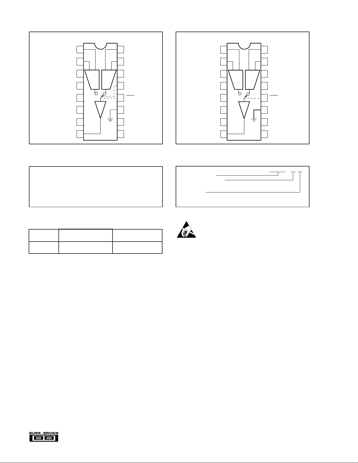
Pin Assignments for Differential ECL Channel Switching Pin Assignments for TTL Channel Switching
+In A
–In A
NC
NC
Compensation
Capacitor
NC
+V
1
2
3
4
5
6
7
CC
+–
AB
+–
16
15
14
13
12
11
10
+In B
–In B
DNC
CHA (ECL)
CHA (ECL)
Common
–V
CC
+In A
–In A
NC
NC
Compensation
Capacitor
NC
+V
1
2
+–
+–
3
AB
4
5
6
7
CC
+In B
16
–In B
15
Short to pin 13
14
Short to pin 14
13
CHA (TTL)
12
Common
11
–V
10
CC
Output
8
9
NC
ABSOLUTE MAXIMUM RATINGS
Supply ............................................................................................. ±7VDC
Differential Input Voltage..............................................................Total V
Input Voltage Range (Analog and Digital)...........................................±V
Storage Temperature Range ....................................... –65°C to +150°C
Lead Temperature (soldering, 10s)............................................... +300°C
Output Short Circuit to Ground (+25°C) ................... Continuous to ground
Junction Temperature .................................................................... +175°C
CC
CC
PACKAGE INFORMATION
PRODUCT PACKAGE NUMBER
PACKAGE DRAWING
OPA678AP 16-Pin Plastic DIP 180
OPA678AU 16-Pin SOIC 211
NOTE: (1) For detailed drawing and dimension table, please see end of data
sheet, or Appendix C of Burr-Brown IC Data Book.
(1)
Output
8
NC
9
ORDERING INFORMATION
Basic Model Number
OPA678
Performance Grade Code
A: –40°C to +85°C
Package Code
P: 16-Pin Plastic DIP
U: 16-Lead SOIC
()()
ELECTROSTATIC
DISCHARGE SENSITIVITY
This integrated circuit can be damaged by ESD. Burr-Brown
recommends that all integrated circuits be handled with
appropriate precautions. Failure to observe proper handling
and installation procedures can cause damage.
ESD damage can range from subtle performance degradation to complete device failure. Precision integrated circuits
may be more susceptible to damage because very small
parametric changes could cause the device not to meet its
published specifications.
®
OPA678 4
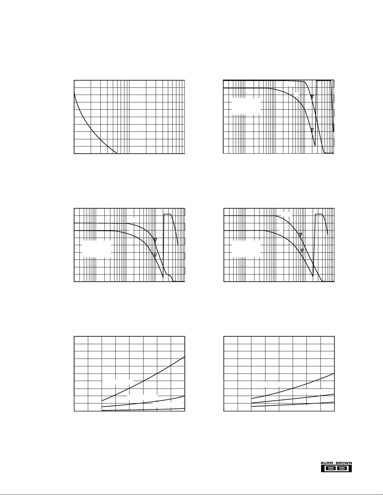
TYPICAL PERFORMANCE CURVES
NOMINAL FREQUENCY COMPENSATION vs NOISE GAIN
10
8
6
4
2
Compensation Capacitor (pF)
0
1 2 100
10468 204080
Noise Gain (V/V)
60
0
–1
–2
–3
–4
–5
–6
Gain (dB)
–7
–8
–9
–10
A
= +1V/V CLOSED-LOOP
V
SMALL SIGNAL BANDWIDTH
Gain
φ
BW = 200MHz
φ
= 57°
= 8.5pF
C
C
1MHz 16Hz
10MHz 100MHz
Frequency (Hz)
0
–20
–40
–60
–80
–100
–120
–140
–160
–180
Phase (°)
8
7
6
5
4
3
2
Gain (dB)
1
0
–1
–2
0.5
0.4
0.3
A
= +2V/V CLOSED-LOOP
V
SMALL SIGNAL BANDWIDTH
Gain
φ
BW = 103MHz
φ
= 103°
= 3pF
C
C
1MHz 16Hz
10MHz 100MHz
Frequency (Hz)
DIFFERENTIAL GAIN vs CLOSED-LOOP GAIN
(f = 4.5MHz)
60
40
20
0
–20
–40
–60
–80
–100
–120
–140
Phase (°)
Gain (dB)
A
= +5V/V CLOSED-LOOP
V
SMALL SIGNAL BANDWIDTH
15
14
Gain
13
12
φ
11
BW = 69MHz
10
φ
= 119°
9
8
C
= 1pF
C
7
6
5
1MHz 16Hz
10MHz 100MHz
Frequency (Hz)
DIFFERENTIAL PHASE vs CLOSED-LOOP GAIN
0.5
(f = 4.5MHz)
0.4
0.3
60
40
20
0
–20
–40
–60
–80
–100
–120
–140
Phase (°)
0.2
Differential Gain (%)
0.1
0
15
VO = 0V to 2.1V
= 0V to 1.4V
V
O
23
V
= 0V to 0.7V
O
4
Closed-Loop Gain
NOTE: For the gain of +2V/V, C
= 2.2pF; for the gain of +5V/V, CC = 0.
C
0.2
Differential Phase (°)
0.1
VO = 0V to 2.1V
0
15
23
Closed-Loop Gain
NOTE: For the gain of +2V/V, C
5
V
= 0V to 1.4V
O
V
= 0V to 0.7V
O
4
= 2.2pF; for the gain of +5V/V, CC = 0.
C
OPA678
®
 Loading...