

Burr Brown OPA660AP, OPA660AU-2K5, OPA660AU Datasheet
© 1990 Burr-Brown Corporation PDS-1072F Printed in U.S.A. April, 1995
Wide Bandwidth
OPERATIONAL TRANSCONDUCTANCE
AMPLIFIER AND BUFFER
APPLICA TIONS
● BASE LINE RESTORE CIRCUITS
● VIDEO/BROADCAST EQUIPMENT
● COMMUNICATIONS EQUIPMENT
● HIGH-SPEED DATA ACQUISITION
● WIDEBAND LED DRIVER
● AGC-MULTIPLIER
● NS-PULSE INTEGRATOR
● CONTROL LOOP AMPLIFIER
● 400MHz DIFFERENTIAL INPUT
AMPLIFIER
FEATURES
● WIDE BANDWIDTH: 850MHz
● HIGH SLEW RATE: 3000V/
µs
● LOW DIFFERENTIAL GAIN/PHASE
ERROR: 0.06%/0.02
°
● VERSATILE CIRCUIT FUNCTION
● EXTERNAL I
Q
-CONTROL
DESCRIPTION
The OPA660 is a versatile monolithic component
designed for wide-bandwidth systems including high
performance video, RF and IF circuitry. It includes a
wideband, bipolar integrated voltage-controlled current source and voltage buffer amplifier.
The voltage-controlled current source or Operational
Transconductance Amplifier (OTA) can be viewed as
an “ideal transistor.” Like a transistor, it has three
terminals—a high-impedance input (base), a lowimpedance input/output (emitter), and the current
output (collector). The OTA, however, is self-biased
and bipolar. The output current is zero-for-zero differential input voltage. AC inputs centered about zero
produce an output current which is bipolar and centered about zero. The transconductance of the OTA
can be adjusted with an external resistor, allowing
bandwidth, quiescent current and gain trade-offs to
be optimized.
The open-loop buffer amplifier provides 850MHz
bandwidth and 3000V/µs slew rate. Used as a basic
building block, the OPA660 simplifies the design of
AGC amplifiers, LED driver circuits for Fiber Optic
Transmission, integrators for fast pulses, fast control
loop amplifiers, and control amplifiers for capacitive
sensors and active filters.
The OPA660 is packaged in SO-8 surface-mount,
and 8-pin plastic DIP, specified from –40°C to +85°C.
OTA
B
E
C
3
8
2
56
+1
100Ω
V
I
200Ω
R
P
82Ω
V
O
R
1
C
P
6.4pF
IQ = 20mA
R
5
100Ω
G = 1 + = 3
R
3
2R
5
X
E
R
3
390Ω
15
10
5
0
–5
–10
–15
–20
–25
1M 10M 100M 1G
Frequency (Hz)
Output Voltage (dB)
OPA660 DIRECT-FEEDBACK FREQUENCY RESPONSE
20
–30
100k
0.2Vp-p
5Vp-p
2.8Vp-p
1.4Vp-p
0.6Vp-p
OPA660
OPA660
OPA660
®
International Airport Industrial Park • Mailing Address: PO Box 11400, Tucson, AZ 85734 • Street Address: 6730 S. Tucson Blvd., Tucson, AZ 85706 • Tel: (520) 746-1111 • Twx: 910-952-1111
Internet: http://www.burr-brown.com/ • FAXLine: (800) 548-6133 (US/Canada Only) • Cable: BBRCORP • Telex: 066-6491 • FAX: (520) 889-1510 • Immediate Product Info: (800) 548-6132

2
®
OPA660
SPECIFICATIONS
Typical at IQ = 20mA, VS = ±5V, TA = +25°C, and RL = 500Ω, unless otherwise specified.
OPA660AP, AU
PARAMETER CONDITIONS MIN TYP MAX UNITS
OTA TRANSCONDUCTANCE
Transconductance V
C
= 0V 75 125 200 mA/V
OTA INPUT OFFSET VOLTAGE V
B
= 0
Initial +10 ±30 mV
vs Temperature 50 µV/°C
vs Supply (tracking) V
S
= ±4.5V to ±5.5V 55 60 dB
vs Supply (non-tracking) V+ = 4.5V to 5.5V 40 45 dB
vs Supply (non-tracking) V– = –4.5V to –5.5V 40 48 dB
OTA B-INPUT BIAS CURRENT
Initial –2.1 ±5 µA
vs Temperature 5 nA/°C
vs Supply (tracking) V
S
= ±4.5V to ±5.5V ±750 nA/V
vs Supply (non-tracking) V+ = 4.5V to 5.5V ±1500 nA/V
vs Supply (non-tracking) V– = –4.5V to –5.5V ±500 nA/V
OTA OUTPUT BIAS CURRENT
Output Bias Current V
B
= 0, VC = 0V ±10 ±20 µA
vs Temperature 500 nA/°C
vs Supply (tracking) V
S
= ±4.5V to ±5.5V ±10 ±25 µA/V
vs Supply (non-tracking) V+ = 4.5V to 5.5V ±10 ±25 µA/V
vs Supply (non-tracking) V– = –4.5V to –5.5V ±10 ±25 µA/V
OTA OUTPUT
Output Current ±10 ± 15 mA
Output Voltage Compliance I
C
= ±1mA ±4.0 ± 4.7 V
Output Impedance 25k || 4.2 Ω || pF
Open-Loop Gain f = 1kHz 70 dB
BUFFER OFFSET VOLTAGE
Initial +7 ±30 mV
vs Temperature 50 µV/°C
vs Supply (tracking) V
S
= ±4.5V to ±5.5V 55 60 dB
vs Supply (non-tracking) V+ = 4.5V to 5.5V 40 45 dB
vs Supply (non-tracking) V– = –4.5V to –5.5V 40 48 dB
BUFFER INPUT BIAS CURRENT
Initial –2.1 ±5 µA
vs Temperature 5 nA/°C
vs Supply (tracking) V
S
= ±4.5V to ±5.5V ±750 nA/V
vs Supply (non-tracking) V+ = 4.5V to 5.5V ±1500 nA/V
vs Supply (non-tracking) V– = –4.5V to –5.5V ±500 nA/V
BUFFER and OTA INPUT IMPEDANCE
Input Impedance 1.0 || 2.1 MΩ || pF
BUFFER INPUT NOISE
Voltage Noise Density, f = 100kHz 4 nV/√Hz
BUFFER DYNAMIC RESPONSE
Small Signal Bandwidth V
O
= ±100mV 850 MHz
Full Power Bandwidth V
O
= ±1.4V 800 MHz
V
O
= ±2.5V 570 MHz
Differential Gain Error 3.58MHz, at 0.7V 0.06 %
Differential Phase Error 3.58MHz, at 0.7V 0.02 Degrees
Harmonic Distortion, 2nd Harmonic f = 10MHz, V
O
= 0.5Vp-p –68 dBc
Slew Rate 5V Step 3000 V/µs
Settling Time 0.1% 2V Step 25 ns
Rise Time (10% to 90%) V
O
= 100mVp-p 1 ns
5V Step 1.5 ns
Group Delay Time 250 ps
BUFFER RATED OUTPUT
Voltage Output I
O
= ±1mA ±3.7 ± 4.2 V
Current Output ±10 ± 15 mA
Gain R
L
= 500Ω 0.96 0.975 V/V
R
L
= 5kΩ 0.99 V/V
Output Impedance 7 || 2 Ω || pF
POWER SUPPLY
Voltage, Rated ±5V
Derated Performance ±4.5 ±5.5 V
Quiescent Current (Programmable, Useful Range) ±3 to ±26 mA

3
®
OPA660
The information provided herein is believed to be reliable; however, BURR-BROWN assumes no responsibility for inaccuracies or omissions. BURR-BROWN assumes
no responsibility for the use of this information, and all use of such information shall be entirely at the user’s own risk. Prices and specifications are subject to change
without notice. No patent rights or licenses to any of the circuits described herein are implied or granted to any third party. BURR-BROWN does not authorize or warrant
any BURR-BROWN product for use in life support devices and/or systems.
ABSOLUTE MAXIMUM RATINGS
Power Supply Voltage .........................................................................±6V
Input Voltage
(1)
........................................................................ ±VS ±0.7V
Operating Temperature ................................................... –40°C to +85°C
Storage Temperature ..................................................... –40°C to +125°C
Junction Temperature .................................................................... +175°C
Lead Temperature (soldering, 10s)............................................... +300°C
NOTE: (1) Inputs are internally diode-clamped to ±V
S
.
Top View DIP/SO-8
I Adjust
E
B
V– = –5V
C
V+ = +5V
Out
In
1
2
3
4
8
7
6
5
Q
1
ELECTROSTATIC
DISCHARGE SENSITIVITY
This integrated circuit can be damaged by ESD. Burr-Brown
recommends that all integrated circuits be handled with
appropriate precautions. Failure to observe proper handling
and installation procedures can cause damage.
ESD damage can range from subtle performance degradation
to complete device failure. Precision integrated circuits may
be more susceptible to damage because very small parametric
changes could cause the device not to meet its published
specifications.
PIN CONFIGURATION
PACKAGE
DRAWING TEMPERATURE
PRODUCT PACKAGE NUMBER
(1)
RANGE
OPA660AP 8-Pin Plastic DIP 006 –25°C to +85°C
OPA660AU SO-8 Surface-Mount 182 –25°C to +85°C
NOTE: (1) For detailed drawing and dimension table, please see end of data
sheet, or Appendix C of Burr-Brown IC Data Book.
PACKAGE/ORDERING INFORMATION
4
®
OPA660
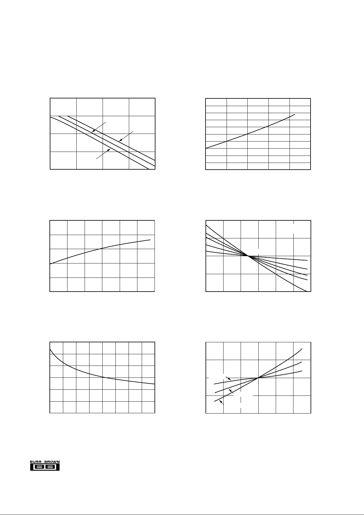
OTA TRANSFER CHARACTERISTICS
10
5
0
–5
–60 –40 –20 0 20 40 60
OTA Input Voltage (mV)
OTA Output Current (mA)
IQ = 20mA
IQ = 5mA
IQ = 10mA
–10
OTA C-OUTPUT RESISTANCE
vs TOTAL QUIESCENT CURRENT (I
Q
)
4
Total Quiescent Current — I
Q
(mA)
OTA Output Resistance (k )
6 8 10 12 14 16 18 20
Ω
60
50
40
30
20
10
0
OTA C-OUTPUT BIAS CURRENT vs TEMPERATURE
–20 –0 20 40 60 80 100
Temperature (°C)
OTA C-Output Bias Current (µA)
Trim Point
5 Representative
Units
–40
–20 40 100
Temperature (°C)
0.0
–1.0
–2.0
–3.0
–4.0
Input Bias Current (µA)
BUFFER AND OTA B-INPUT BIAS CURRENT
vs TEMPERATURE
80
–0 20 60
–5.0
TOTAL QUIESCENT CURRENT vs TEMPERATURE
–25 25 100
Temperature (°C)
1.5
1.4
1.3
1.2
1.1
1.0
0.9
0.8
0.7
0.6
Total Quiescent Current (Normalized)
05075
0.5
TYPICAL PERFORMANCE CURVES
IQ = 20mA, TA = +25°C, and VS = ±5V unless otherwise noted.
100 1.0k 10k
R — Resistor Value ( )
Q
Ω
100
30
10
3.0
Total Quiescent Current (mA)
TOTAL QUIESCENT CURRENT vs R
Q
300 3.0k
1.0
Nominal
Device
Low I
Q
Device
High I
Q
Device
5
®
OPA660
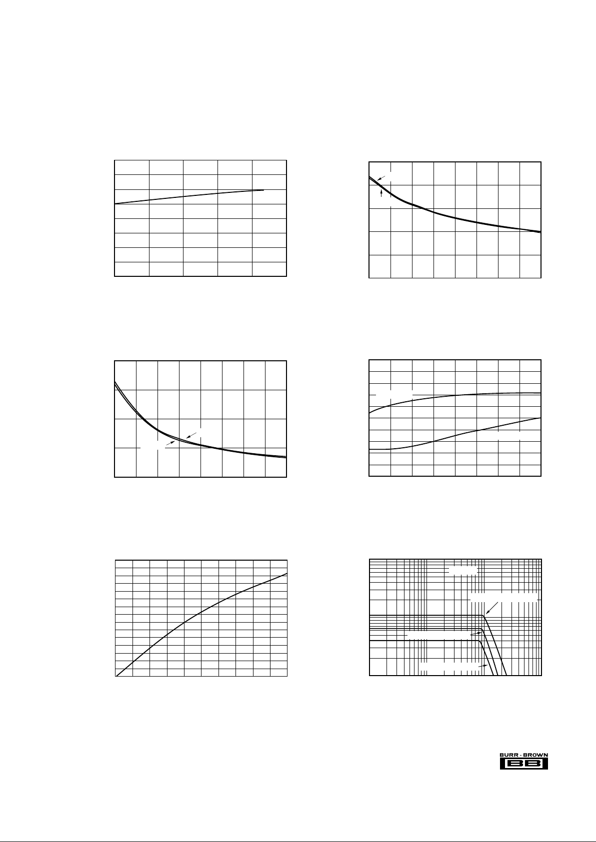
OTA TRANSCONDUCTANCE vs FREQUENCY
1M 10M
100M
1G
1000
100
OTA Transconductance (mA/V)
Frequency (Hz)
IQ = 20mA 106mA/V
IQ = 10mA 66mA/V
IQ = 5mA 40mA/V
RL = 50Ω
10
BUFFER SLEW RATE
vs TOTAL QUIESCENT CURRENT (I
Q
)
4
Total Quiescent Current—I
Q
(mA)
4000
3800
3600
3400
3200
3000
2800
2600
2400
2200
Slew Rate (V/µs)
6 8 10 12 14 16 18 20
Rising Edge
Falling Edge
2000
BUFFER OUTPUT AND OTA E-OUTPUT RESISTANCE
vs TOTAL QUIESCENT CURRENT (I
Q
)
Total Quiescent Current—I
Q
(mA)
Buffer Output and OTA E-Output Resistance (Ω)
4 6 8 10 12 14 16 18 20
40
30
20
10
0
R
OUTBUF
R
OUTOTA
BUFFER AND OTA B-INPUT RESISTANCE
vs TOTAL QUIESCENT CURRENT (I
Q
)
4
Total Quiescent Current — I (mA)
Buffer and OTA B-Input Resistance (MΩ)
6 8 10 12 14 16 18 20
Q
4
3
2
1
0
–1
R
INOTA
R
INBUF
BUFFER AND OTA B-INPUT OFFSET VOLTAGE
vs TEMPERATURE
–25
Temperature (°C)
20
15
10
5
0
–5
–10
–15
Offset Voltage (mV)
0 255075100
–20
TYPICAL PERFORMANCE CURVES (CONT)
IQ = 20mA, TA = +25°C, and VS = ±5V unless otherwise noted.
OTA TRANSCONDUCTANCE
vs TOTAL QUIESCENT CURRENT (I
Q
)
0
Total Quiescent Current—I
Q
(mA)
150
100
50
OTA Transconductance (mA/V)
4 6 8 1012 161820
0
214
6
®
OPA660
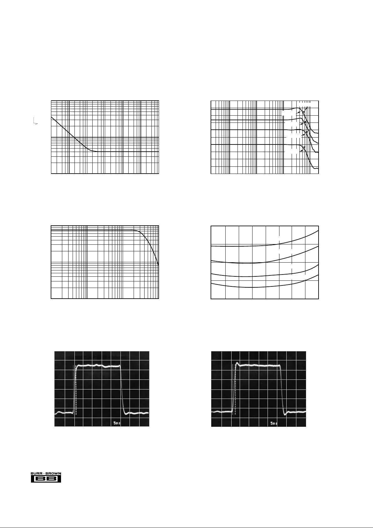
TRANSCONDUCTANCE vs INPUT VOLTAGE
160
120
80
40
0
–40 –30 –20 –10 0 10 20 30 40
RQ = 250Ω
RQ = 500Ω
R
Q
= 1kΩ
R
Q
= 2kΩ
Input Voltage (mV)
BUFFER MAX OUTPUT VOLTAGE vs FREQUENCY
10
0
Buffer Output Voltage (Vp-p)
1M 10M 100M 1G
Frequency (Hz)
0.1
15
10
5
0
–5
–10
–15
–20
–25
1M 10M 100M 1G
Frequency (Hz)
Output Voltage (dB)
0.2Vp-p
0.6Vp-p
1.4Vp-p
–3dB Point
I
Q
= 20mA RIN = 160Ω RL = 100Ω
20
BUFFER FREQUENCY RESPONSE
dB
2.8Vp-p
200k
BUFFER VOLTAGE NOISE SPECTRAL DENSITY
100
10
100 1k 10k 100k 1M 10M 100M
Frequency (Hz)
Voltage Noise (nV/ Hz)
1
TYPICAL PERFORMANCE CURVES (CONT)
IQ = 20mA, TA = +25°C, and VS = ±5V unless otherwise noted.
Transconductance (mA/V)
OTA PULSE RESPONSE
Output Voltage = 5Vp-p
–2.5V
+2.5V
0V
V
O
(V)
OTA PULSE RESPONSE
Input Voltage = 1.25Vp-p, t
R
= tF = 1ns, Gain = 4
–0.625V
+0.625V
0V
V
O
(V)
 Loading...