

Burr Brown OPA655U-2K5, OPA655U, OPA655P Datasheet
© 1994 Burr-Brown Corporation PDS-1271D Printed in U.S.A. May, 1997
DESCRIPTION
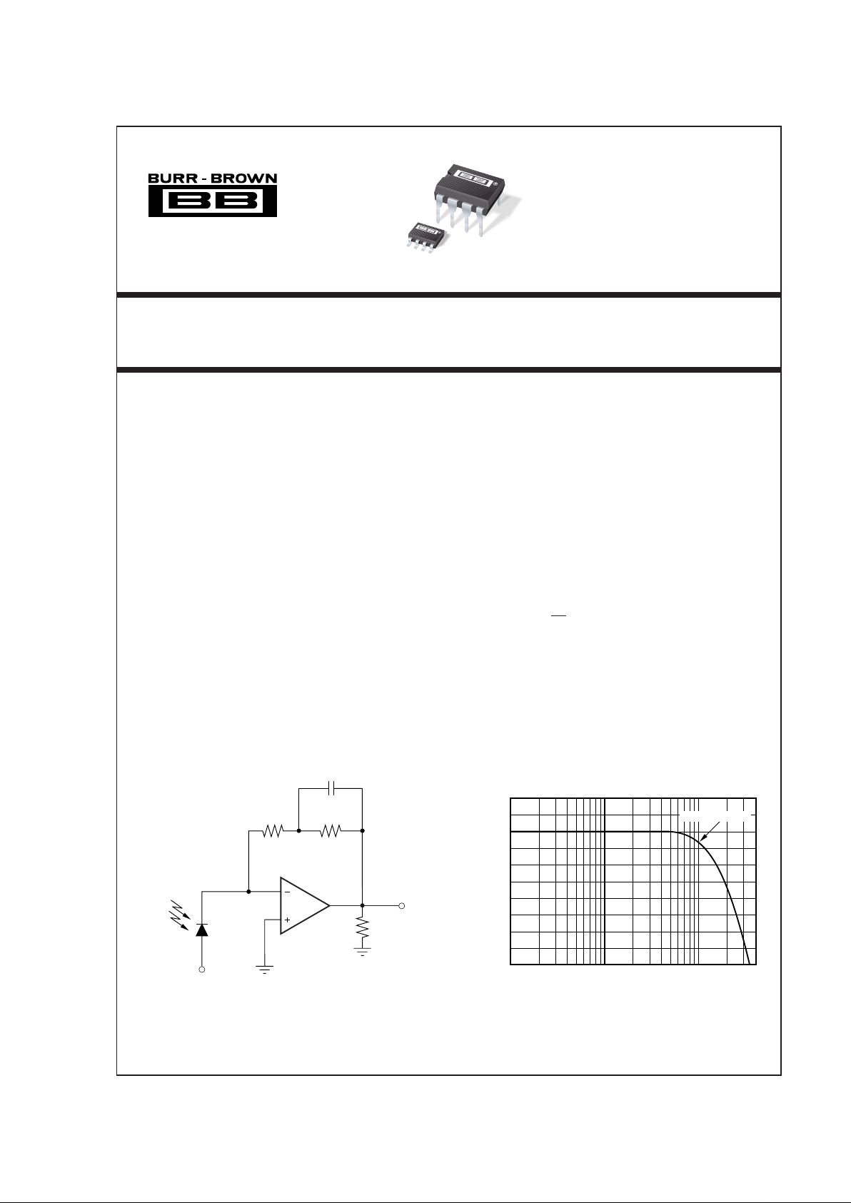
The OPA655 combines a very wideband, unity gain
stable, voltage feedback op amp with a FET input
stage to offer an ultra high dynamic range amplifier
for ADC buffering and transimpedance applications.
Extremely low harmonic distortion along with excellent pulse settling characteristics will support even the
most demanding ADC input buffer requirements.
The broad unity gain stable bandwidth and FET input
allows exceptional performance in high speed, low
noise integrators.
The high input impedance and low bias current provided by the FET input is further supported by the
ultra-low 6nV/√Hz input voltage noise to achieve a
very low integrated noise in wideband photodiode
transimpedance applications.
Broad transimpedance bandwidths are achievable given
the OPA655’s high 240MHz gain bandwidth product.
As shown below, a –3dB bandwidth of 1MHz is
provided even for a high 1MΩ transimpedance gain
from a 47pF source capacitance.
FEATURES
● 400MHz UNITY GAIN BANDWIDTH
● LOW INPUT BIAS CURRENT: 5pA
● HIGH INPUT IMPEDANCE: 10
12
Ω || 1.0pF
● ULTRA-LOW dG/dP: 0.006%/0.009
°
● LOW DISTORTION: 90dB SFDR at 5MHz
● FAST SETTLING: 17ns (0.01%)
● HIGH OUTPUT CURRENT: 60mA
● FAST OVERDRIVE RECOVERY
Wideband, Unity Gain Stable, FET-Input
OPERATIONAL AMPLIFIER
OPA655
APPLICATIONS
● WIDEBAND PHOTODIODE
AMPLIFIER
● PEAK DETECTOR
● CCD OUTPUT BUFFER
● ADC INPUT BUFFER
● HIGH SPEED INTEGRATOR
● TEST AND MEASUREMENT FRONT END
®
Frequency
1MΩ TRANSIMPEDANCE BANDWIDTH
130
120
110
100
90
80
10kHz 100kHz 1MHz 5MHz
Transimpedance Gain (dB)
1MHz Bandwidth
OPA655
Wideband Photodiode Transimpedance Amplifier
(47pF)
λ
–V
b
499kΩ499kΩ
V
O
100Ω
1pF
International Airport Industrial Park • Mailing Address: PO Box 11400, Tucson, AZ 85734 • Street Address: 6730 S. Tucson Blvd., Tucson, AZ 85706 • Tel: (520) 746-1111 • Twx: 910-952-1111
Internet: http://www.burr-brown.com/ • FAXLine: (800) 548-6133 (US/Canada Only) • Cable: BBRCORP • Telex: 066-6491 • FAX: (520) 889-1510 • Immediate Product Info: (800) 548-6132
OPA655
OPA655
®
OPA655
2
SPECIFICATIONS
At TA = +25°C, VS = ±5V, R
FB
= 100Ω, and RL = 100Ω, unless otherwise noted. R
FB
= 0 for G = +1.
OPA655P, U
PARAMETER CONDITIONS MIN TYP MAX UNITS
The information provided herein is believed to be reliable; however, BURR-BROWN assumes no responsibility for inaccuracies or omissions. BURR-BROWN assumes
no responsibility for the use of this information, and all use of such information shall be entirely at the user’s own risk. Prices and specifications are subject to change
without notice. No patent rights or licenses to any of the circuits described herein are implied or granted to any third party. BURR-BROWN does not authorize or warrant
any BURR-BROWN product for use in life support devices and/or systems.
FREQUENCY RESPONSE
Closed-Loop Response Gain = +1V/V, V
O
= 200mVp-p 400 MHz
Gain = +2V/V, V
O
= 200mVp-p 185 MHz
Gain = +5V/V, V
O
= 200mVp-p 57 MHz
Gain = +10V/V, V
O
= 200mVp-p 24 MHz
Gain-Bandwidth Product 240 MHz
Slew Rate G = +1, 1V Step 210 290 V/µs
Over Temperature 200 V/µs
Rise Time 0.2V Step 1 ns
Fall Time 0.2V Step 1 ns
Settling Time: 0.01% G = +1, 1V Step 17 ns
0.1% G = +1, 1V Step 8 ns
1% G = +1, 1V Step 6 ns
Spurious-Free Dynamic Range G = +1, f = 5MHz 75 90 dBc
V
O
= ±1V, RL = 100Ω
Differential Gain 3.58MHz, 0 to 1.4V, R
L
= 150Ω 0.006 %
Differential Phase 3.58MHz, 0 to 1.4V, R
L
= 150Ω 0.009 degrees
Bandwidth for 0.1dB flatness G = +2, 2Vp-p 30 MHz
OFFSET VOLTAGE
Input Offset Voltage ±1 ±2mV
Over Temperature ±10 µV/°C
Power Supply Rejection (+V
S
)|V
S
| = 4.50V to 5.50V 55 70 dB
(–V
S
)5065dB
INPUT BIAS CURRENT
(1)
Input Bias Current VCM = 0V –5 –125 pA
Over Temperature V
CM
= 0V –8.0 nA
Input Offset Current V
CM
= 0V ±2 ±125 pA
Over Temperature V
CM
= 0V ±8nA
NOISE
Input Voltage Noise
Noise Density: f = 100Hz 20 nV/√Hz
f = 1kHz 8 nV/√Hz
f = 10kHz 6 nV/√Hz
f = 0.1MHz to 100MHz 6 nV/√Hz
Integrated Voltage Noise,
BW = 1MHz to 100MHz 60 µVrms
Input Bias Current Noise
Current Noise Density,
f = 10Hz to 10kHz 1.3 4 fA/√Hz
INPUT VOLTAGE RANGE
Common-Mode Input Range ±2.75 V
Over Temperature ±2.5 V
Common-Mode Rejection V
CM
= ±0.5V 55 70 dB
INPUT IMPEDANCE
Differential
10
12
|| 1.2
Ω || pF
Common-Mode
10
12
|| 1.0
Ω || pF
OPEN-LOOP GAIN
Open-Loop Voltage Gain V
O
= ±2V, RL = 100Ω 53 58 dB
Over Temperature V
O
= ±2V, RL = 100Ω 50 dB
OUTPUT
Voltage Output R
L
= 100Ω, G = +1 ±3.0 ±3.4 V
Over Temperature ±2.8 V
Current Output ±35 ±60 mA
Over Temperature ±28 mA
Short-Circuit Output Current ±140 mA
Output Resistance 0.1MHz, G = +1 0.04 Ω
POWER SUPPLY
Specified Operating Voltage ±5V
Operating Voltage Range T
MIN
to T
MAX
±4.75 ±5.25 V
Quiescent Current T
MIN
to T
MAX
±21 ±25 ±29 mA
Over Temperature ±31 mA
TEMPERATURE RANGE
Specification: P, U –40 +85 °C
Thermal Resistance,
θ
JA
P 100 °C/W
U 125 °C/W
NOTE: (1) Junction temperature ≈ +25°C for room temperature tested input bias and offset current.
3
®
OPA655
Total Supply Voltage Across Device (V
S (TOTAL)
) ................................11V
Internal Power Dissipation ........................... See Thermal Considerations
Differential Input Voltage ............................................................ V
S (TOTAL)
Common-Mode Input Voltage Range .................................................. ±V
S
Storage Temperature Range: P, U ............................... –40°C to +125°C
Lead Temperature (soldering, 10s) .............................................. +300°C
(soldering, SO-8, 3s) ...................................... +260°C
Junction Temperature (T
J
) ............................................................ +175°C
ABSOLUTE MAXIMUM RATINGS
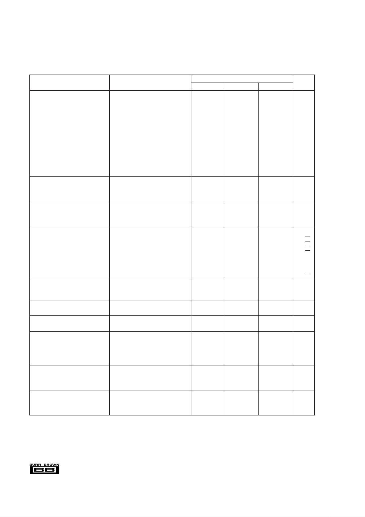
PIN CONFIGURATION
PACKAGE DRAWING
PRODUCT PACKAGE NUMBER
(1)
OPA655P 8-Pin Plastic DIP 006
OPA655U SO-8 182
NOTE: (1) For detailed drawing and dimension table, please see end of data
sheet, or Appendix C of Burr-Brown IC Data Book.
PACKAGE INFORMATION
Top View DIP/SO-8
PRODUCT PACKAGE TEMPERATURE RANGE
OPA655P 8-Pin Plastic DIP –40°C to +85°C
OPA655U SO-8 –40°C to +85°C
ORDERING INFORMATION
ELECTROSTATIC
DISCHARGE SENSITIVITY
Electrostatic discharge can cause damage ranging from performance degradation to complete device failure. Burr-Brown
Corporation recommends that all integrated circuits be handled
and stored using appropriate ESD protection methods.
ESD damage can range from subtle performance degradation
to complete device failure. Precision integrated circuits may
be more susceptible to damage because very small parametric
changes could cause the device not to meet published specifications.
NOTE: (1) Making use of all four power supply pins is highly recommended,
although not required. Using these four pins, instead of pins 4 and 7 only, will
reduce the effective pin impedance and substantially improve distortion.
1
2
3
4
8
7
6
5
+V
S2
(1)
+V
S1
Output
–V
S2
(1)
NC
Inverting Input
Non-Inverting Input
–V
S1

®
OPA655
4
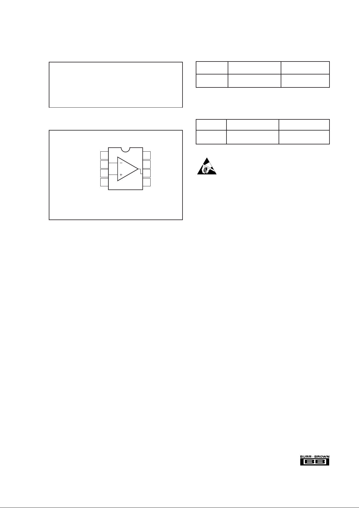
TYPICAL PERFORMANCE CURVES
At TA = +25°C, VS = ±5V, R
FB
= 100Ω, and RL = 100Ω, unless otherwise noted. R
FB
= 0 for G = +1.
INPUT VOLTAGE AND CURRENT NOISE
100
10
1
10 100 1k 10k 100k 1M 10M 100M
Input Voltage Noise (nV/√Hz)
Input Current Noise (fA/√Hz)
Frequency (Hz)
Voltage Noise
Current Noise
INPUT BIAS AND OFFSET CURRENT
vs TEMPERATURE
1000
100
10
1
–50 0 50
I
B
100
Offset Current (pA)
Input Bias Current (pA)
Temperature (°C)
IOS
CLOSED-LOOP BANDWIDTH
1M 10M 100M 1G 3G
Frequency (Hz)
6
3
0
–3
–6
–9
–12
Gain (dB)
Bandwidth
= 400MHz
SO-8DIP
G = +1
CLOSED-LOOP BANDWIDTH
100k 1M 10M 100M 1G
Frequency (Hz)
12
9
6
3
0
–3
–6
–9
–12
Gain (dB)
G = +2
DIP, SO-8
Bandwidth = 185MHz
CLOSED-LOOP BANDWIDTH
100k 1M 10M 100M 1G
Frequency (Hz)
20
17
14
11
8
5
–2
–1
–4
Gain (dB)
G = +5
DIP, SO-8
Bandwidth = 57MHz
CLOSED-LOOP BANDWIDTH
100k 1M 10M 100M 1G
Frequency (Hz)
26
23
20
17
14
11
8
5
2
Gain (dB)
G = +10
DIP, SO-8
Bandwidth = 24MHz
5
®
OPA655
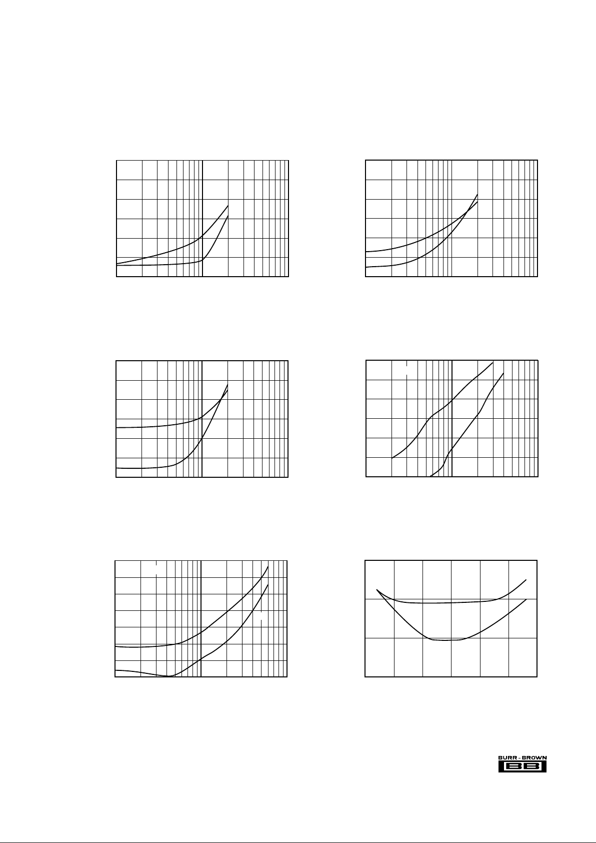
TYPICAL PERFORMANCE CURVES (CONT)
At TA = +25°C, VS = ±5V, R
FB
= 100Ω, and RL = 100Ω, unless otherwise noted. R
FB
= 0 for G = +1.
HARMONIC DISTORTION vs TEMPERATURE
(V
O
= 2Vp-p, G = +1, fO = 5MHz)
–50 –25 0 25 50 75 100
Temperature (°C)
–85
–90
–95
–100
Harmonic Distortion (dBc)
2f
O
3f
O
HARMONIC DISTORTION vs FREQUENCY
(V
O
= 2Vp-p, G = +1)
1M 10M
2f
O
3f
O
100M
Frequency (Hz)
–40
–50
–60
–70
–80
–90
–100
Harmonic Distortion (dBc)
HARMONIC DISTORTION vs FREQUENCY
(V
O
= 2Vp-p, G = +2)
1M 10M 100M
Frequency (Hz)
–40
–50
–60
–70
–80
–90
–100
Harmonic Distortion (dBc)
2f
O
3f
O
HARMONIC DISTORTION vs FREQUENCY
(V
O
= 2Vp-p, G = +5)
1M 10M 100M
Frequency (Hz)
–40
–50
–60
–70
–80
–90
–100
Harmonic Distortion (dBc)
2f
O
3f
O
5MHz HARMONIC DISTORTION
vs OUTPUT SWING
0.1 1 10
Output Swing (Vp-p)
–85
–90
–95
–100
–105
–110
–115
Harmonic Distortion (dBc)
2f
O
3f
O
G = +1
10MHz HARMONIC DISTORTION
vs OUTPUT SWING
0.1 1 10
Output Swing (Vp-p)
–60
–65
–70
–75
–80
–85
–90
–95
Harmonic Distortion (dBc)
2f
O
3f
O
G = +1
 Loading...