

Burr Brown OPA651U-2K5, OPA651U Datasheet
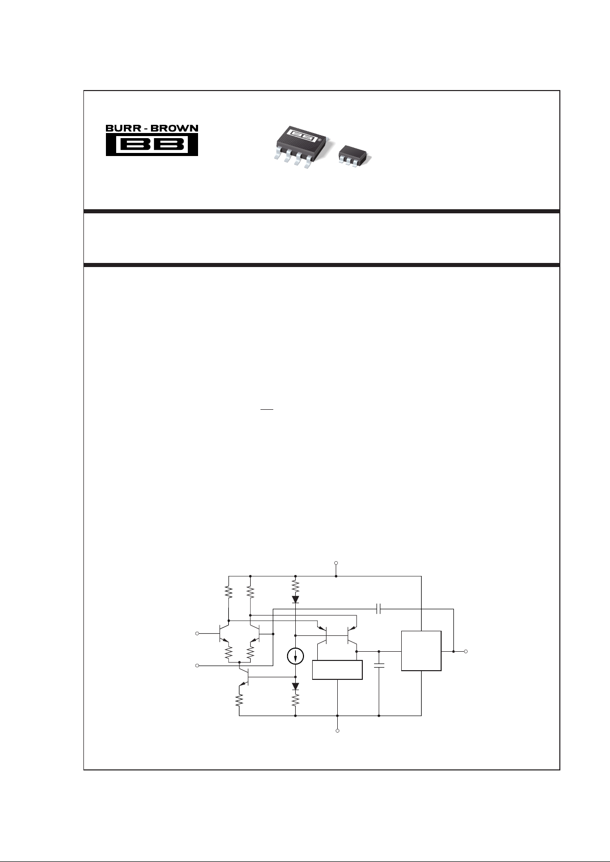
DESCRIPTION
The OPA651 is a low power, wideband voltage feedback operational amplifier. It features a bandwidth at
G = +2 of 470MHz as well as a 12-bit settling time of
only 16ns. The wide bandwidth and true differential
input stage make it suitable for use in a variety of
applications. Its low distortion gives exceptional performance for telecommunications, medical imaging
and video applications.
The OPA651 is compensated for stability in gains of
two or more, differentiating it from the unity gain
stable OPA650. Its unusual combination of speed,
accuracy and low power make it an outstanding choice
for many portable, multi-channel and other high speed
applications, where power is at a premium.
Wideband, Low Power Voltage Feedback
OPERATIONAL AMPLIFIER
© 1994 Burr-Brown Corporation PDS-1265E Printed in U.S.A. March, 1998
OPA651
®
FEATURES
● STABLE IN GAINS: ≥ 2V/V
● LOW POWER: 50mW
● BANDWIDTH: 470MHz at G = 2
● FAST SETTLING TIME: 16ns to 0.01%
● LOW HARMONICS: –78dB at 5MHz
● LOW INPUT BIAS CURRENT: 4
µA
● DIFFERENTIAL GAIN/PHASE ERROR:
0.01%/0.025
°
● LOW VOLTAGE NOISE: 4.6nV/√Hz
APPLICATIONS
● HIGH RESOLUTION VIDEO
● MONITOR PREAMPLIFIER
● CCD IMAGING AMPLIFIER
● ULTRASOUND SIGNAL PROCESSING
● ADC/DAC GAIN AMPLIFIER
● BASEBAND SIGNAL PROCESSING
Current
Mirror
Output
Stage
C
C
Inverting
Input
Non-Inverting
Input
+V
S
Output
–V
S
1.5pF
International Airport Industrial Park • Mailing Address: PO Box 11400, Tucson, AZ 85734 • Street Address: 6730 S. Tucson Blvd., Tucson, AZ 85706 • Tel: (520) 746-1111 • Twx: 910-952-1111
Internet: http://www.burr-brown.com/ • FAXLine: (800) 548-6133 (US/Canada Only) • Cable: BBRCORP • Telex: 066-6491 • FAX: (520) 889-1510 • Immediate Product Info: (800) 548-6132
OPA651
2OPA651
®
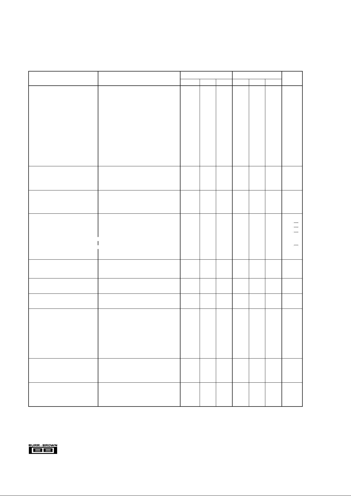
SPECIFICATIONS
At TA = +25°C, VS = ±5V, RL = 100Ω, RFB = 402Ω, G = +2, unless otherwise noted.
OPA651U, N OPA651UB, NB
PARAMETER CONDITIONS MIN TYP MAX MIN TYP MAX UNITS
FREQUENCY RESPONSE
Closed-Loop Bandwidth
(2)
G = +2 470 *
(1)
MHz
G = +5 70 * MHz
G = +10 34 * MHz
Gain Bandwidth Product 340 * MHz
Slew Rate G = +2, V
O
= 2V step 300 * V/µs
Over Specified Temperature 275 * V/µs
Rise Time 0.2V Step 0.8 * ns
Fall Time 0.2V Step 0.8 * ns
Settling Time 0.01% G = +2, V
O
= 2V step 16.2 * ns
0.1% G = +2, V
O
= 2V step 11.5 * ns
1% G = +2, V
O
= 2V step 7.2 * ns
Spurious Free Dynamic Range G = +2, f = 5.0 MHz, V
O
= 2Vp-p,
R
L
= 100Ω 67 * dBc
R
L
= 400Ω 78 * dBc
Differential Gain G = +2, NTSC, V
O
= 1.4Vp, RL = 150Ω 0.01 * %
Differential Phase G = +2, NTSC, V
O
= 1.4Vp, RL = 150Ω 0.025 * Degrees
Bandwidth For 0.1dB Flatness G = +2 43 * MHz
INPUT OFFSET VOLTAGE
Input Offset Voltage ±1 ±5.0 * ±2.0 mV
Average Drift ±3*µV/°C
Power Supply Rejection (+V
S
)V
S
= ±4.5V to ±5.5V 65 85 70 * dB
(–V
S
)526055*dB
INPUT BIAS CURRENT
Input Bias Current V
CM
= 0V 4 20 * 10 µA
Over Temperature 630 *20 µA
Input Offset Current V
CM
= 0V 0.4 1.5 * * µA
Over Temperature 0.9 3.0 * * µA
INPUT NOISE
Input Voltage Noise
Noise Density, f = 100Hz 13 * nV/√Hz
f = 10kHz 4.6 * nV/√Hz
f = 1MHz 4.6 * nV/√Hz
Voltage Noise, BW = 10Hz to 100MHz 46 * µVrms
Input Bias Current Noise
Current Noise Density, f = 0.1Hz to 20kHz 1.1 * pA/√Hz
Noise Figure (NF) R
S
= 10kΩ 3.2 * dB
R
S
= 50Ω 14 * dB
INPUT VOLTAGE RANGE
Common-Mode Input Range ±3.5 * V
Over Specified Temperature ±3.0 * V
Common-Mode Rejection V
CM
= ±0.5V 75 90 80 * dB
INPUT IMPEDANCE
Differential 60 || 1 * kΩ || pF
Common-Mode 2.6 || 1 * MΩ || pF
OPEN-LOOP GAIN
Open-Loop Voltage Gain V
O
= ±2V, RL = 100Ω 42 50 45 * dB
Over Specified Temperature V
O
= ±2V, RL = 100Ω 40 42 dB
OUTPUT
Voltage Output
Over Specified Temperature No Load ±2.2 ±3.0 ±2.4 * V
R
L
= 250Ω±2.2 ±2.5 ±2.4 * V
R
L
= 100Ω±2.0 ±2.3 ±2.1 * V
Current Output, Sourcing 75 110 * * mA
Over Specified Temperature 65 * mA
Current Output, Sinking 65 85 * * mA
Over Specified Temperature 35 * mA
Short Circuit Current 150 * mA
Output Resistance 0.1MHz, G = +2 0.05 * Ω
POWER SUPPLY
Specified Operating Voltage ±5*V
Operating Voltage Range ±4.5 ±5.5 * * V
Quiescent Current ±5.1 ±7.75 * ±6.5 mA
Over Specified Temperature ±8.75 ±7.5 mA
TEMPERATURE RANGE
Specification: U, N, UB, NB –40 +85 * * °C
Thermal Resistance,
θ
JA
U SO-8 125 * °C/W
N SOT23-5 150 * °C/W
NOTES: (1) An asterisk (*) specifies the same value as the grade to the left. (2) Frequency response can be strongly influenced by PC board parasitics. The OPA651
is nominally compensated assuming 2pF parasitic load. The demonstration boards show low parasitic layouts for the different package styles.
3 OPA651
®
1
2
3
54+V
S
–Input
Output
–V
S
+Input
1
2
3
4
8
7
6
5
NC
+V
S
Output
NC
NC
–Input
+Input
–V
S
PIN CONFIGURATION
Top View SO-8
Supply ...............................................................................................±5.5V
Internal Power Dissipation
(1)
: .............................. See Thermal Conditions
Differential Input Voltage .................................................................. ±1.2V
Input Voltage Range ............................................................................ ±V
S
Storage Temperature Range: U, UB, N, NB ................ –40°C to +125°C
Lead Temperature (soldering, 10s) .............................................. +300°C
(soldering, SO-8 3s) ...................................................................... +260°C
Junction Temperature (T
J
) ............................................................ +175°C
ABSOLUTE MAXIMUM RATINGS
SOT23-5
ELECTROSTATIC
DISCHARGE SENSITIVITY
Electrostatic discharge can cause damage ranging from performance degradation to complete device failure. Burr-Brown
Corporation recommends that all integrated circuits be handled
and stored using appropriate ESD protection methods.
ESD damage can range from subtle performance degradation
to complete device failure. Precision integrated circuits may
be more susceptible to damage because very small parametric
changes could cause the device not to meet published specifications.
PACKAGE
DRAWING TEMPERATURE PACKAGE ORDERING
PRODUCT PACKAGE NUMBER
(1)
RANGE MARKING
(2)
NUMBER
(3)
OPA651U SO-8 Surface Mount 182 –40°C to +85°C OPA651U OPA651U
OPA651UB SO-8 Surface Mount 182 –40°C to +85°C OPA651UB OPA651UB
OPA651N 5-pin SOT23-5 331 –40°C to +85°C A51 OPA651N-250
OPA651N-3k
OPA651NB 5-pin SOT23-5 331 –40°C to +85°C A51B OPA651NB-250
OPA651NB-3k
NOTE: (1) For detailed drawing and dimension table, please see end of data sheet, or Appendix C of Burr-Brown IC Data Book. (2) The “B” grade of the SO-8 package
will be marked with a “B” by pin 8. The “B” grade of the SOT23-5 will be marked with a “B” near pins 3 and 4. (3) The SOT23-5 is only available on a 7" tape and reel
(e.g. ordering 250 pieces of “OPA651N-250” will get a single 250 piece tape and reel. Ordering 3000 pieces of “OPA651N-3k” will get a single 3000 piece tape and reel).
Please refer to Appendix B of Burr-Brown IC Data Book for detailed Tape and Reel Mechanical information.
PACKAGE/ORDERING INFORMATION
The information provided herein is believed to be reliable; however, BURR-BROWN assumes no responsibility for inaccuracies or omissions. BURR-BROWN assumes
no responsibility for the use of this information, and all use of such information shall be entirely at the user’s own risk. Prices and specifications are subject to change
without notice. No patent rights or licenses to any of the circuits described herein are implied or granted to any third party. BURR-BROWN does not authorize or warrant
any BURR-BROWN product for use in life support devices and/or systems.
4OPA651
®
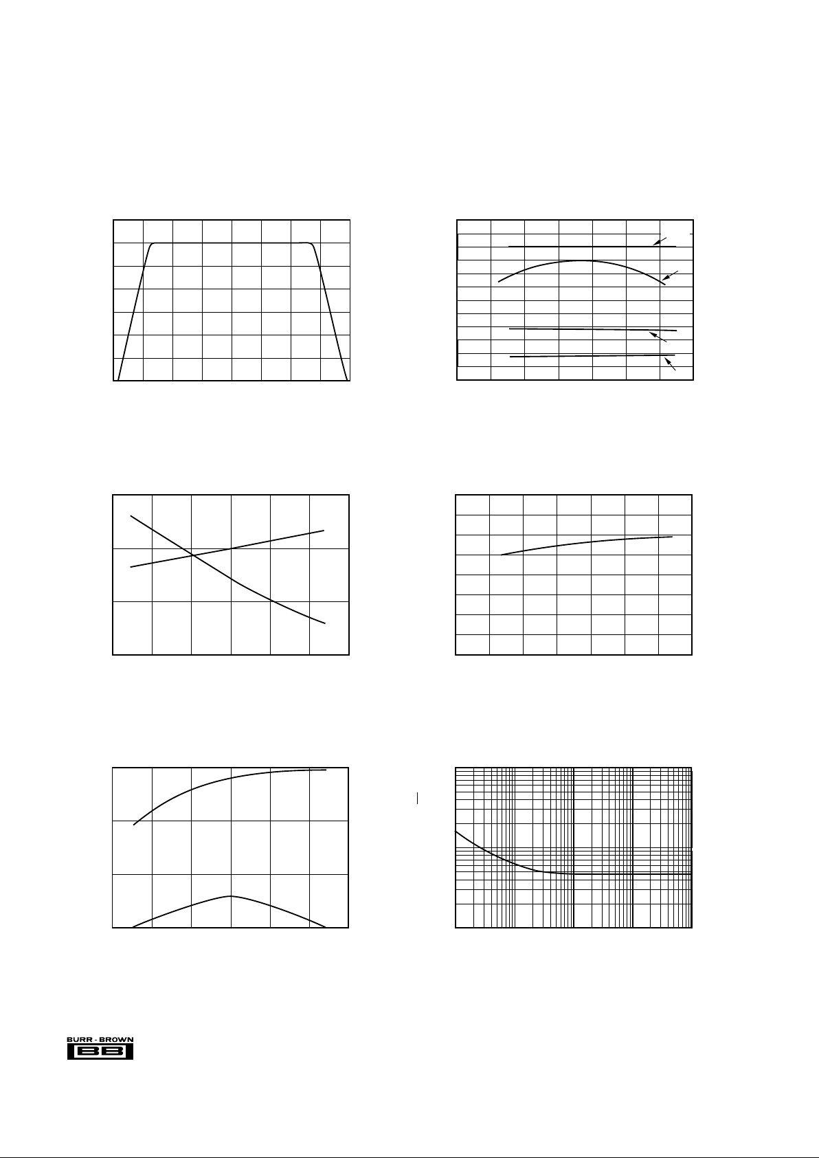
TYPICAL PERFORMANCE CURVES
At TA = +25°C, VS = ±5V, RL = 100Ω, RFB = 402Ω, and G = +2, unless otherwise noted.
OUTPUT CURRENT vs TEMPERATURE
110
100
90
80
–50 –25 0 25 50 75 100
Output Current (±mA)
Temperature (°C)
I
O
+
I
O
–
INPUT VOLTAGE NOISE DENSITY vs FREQUENCY
100 1k 10k 100k 1M
Input Voltage Noise (nV/√Hz)
Frequency (Hz)
100
10
1
SUPPLY CURRENT vs TEMPERATURE
8
7
6
5
4
3
2
1
0
–75 –50 –25 0 25 50 75 100
Supply Current (±mA)
Ambient Temperature (°C)
INPUT BIAS CURRENT AND OFFSET VOLTAGE
vs TEMPERATURE
7
6
5
4
2
1
0
–1
–50 –25 0 25 50 75 100
Input Bias Current (mA)
Offset Voltage (mV)
Temperature (°C)
V
OS
I
B
COMMON-MODE REJECTION RATIO
vs COMMON-MODE INPUT VOLTAGE
100
90
80
70
60
50
40
30
–4 –2–3 –101234
Common-Mode Rejection (dB)
Common-Mode Voltage (V)
AOL, PSR+, PSR–, AND CMRR vs TEMPERATURE
100
95
90
85
80
75
70
65
60
55
50
45
40
–75 –50 –25 0 25 50 75 100
A
OL
, PSR+, PSR–, and CMRR (dB)
Ambient Temperature (°C)
A
OL
PSR+
PSR–
CMRR
 Loading...