

Burr Brown OPA643N-250, OPA643NB-3K, OPA643U, OPA643UB, OPA643NB-250 Datasheet
...
®
OPA643
1
Wideband Low Distortion, High Gain
OPERATIONAL AMPLIFIER
®
OPA643
APPLICATIONS
● BASE STATION ADC PREAMP
● ADC/DAC BUFFER AMPLIFIER
● LOW DISTORTION IF AMPLIFIER
● LOW NOISE, BROADBAND,
TRANSIMPEDANCE AMPLIFIER
● LOW NOISE PREAMPLIFIER
● VIDEO AMPLIFICATION
● TEST INSTRUMENTATION
OPA643
OPA658
OPA643
International Airport Industrial Park • Mailing Address: PO Box 11400, Tucson, AZ 85734 • Street Address: 6730 S. Tucson Blvd., Tucson, AZ 85706 • Tel: (520) 746-1111 • Twx: 910-952-1111
Internet: http://www.burr-brown.com/ • FAXLine: (800) 548-6133 (US/Canada Only) • Cable: BBRCORP • Telex: 066-6491 • FAX: (520) 889-1510 • Immediate Product Info: (800) 548-6132
FEATURES
● LOW DISTORTION: –90dBc at 5MHz
● LOW NOISE: 2.3nV/√Hz
● GAIN-BANDWIDTH PRODUCT: 800MHz
● AVAILABLE IN SOT23-5 PACKAGE
● STABLE IN GAINS
≥ 3
● HIGH SLEW RATE: 1000V/
µs
● HIGH OPEN-LOOP GAIN: 95dB
● HIGH OUTPUT CURRENT:
±60mA
DESCRIPTION
The OPA643 provides a level of speed and dynamic
range previously unattainable in a monolithic op amp.
Using a de-compensated voltage feedback architecture with two internal gain stages, the OPA643 achieves
exceptionally low harmonic distortion over a wide
frequency range. The "classic" differential input provides all the familiar benefits of precision op amps,
such as bias current cancellation and very low inverting current noise compared with wideband current
feedback op amps. High slew rate and open-loop gain,
along with low input noise and high output current
drive make the OPA643 ideal for very high dynamic
range requirements.
The high gain bandwidth product for the gain ≥ 3
stable OPA643 makes it particularly suitable for
wideband transimpedance amplifiers and moderate gain
IF amplifier applications. External compensation
techniques may be used to apply the OPA643 at low
gains giving exceptionally low distortion and frequency
response flatness. Where unity gain stability with
comparable distortion performance is required, consider
the OPA642.
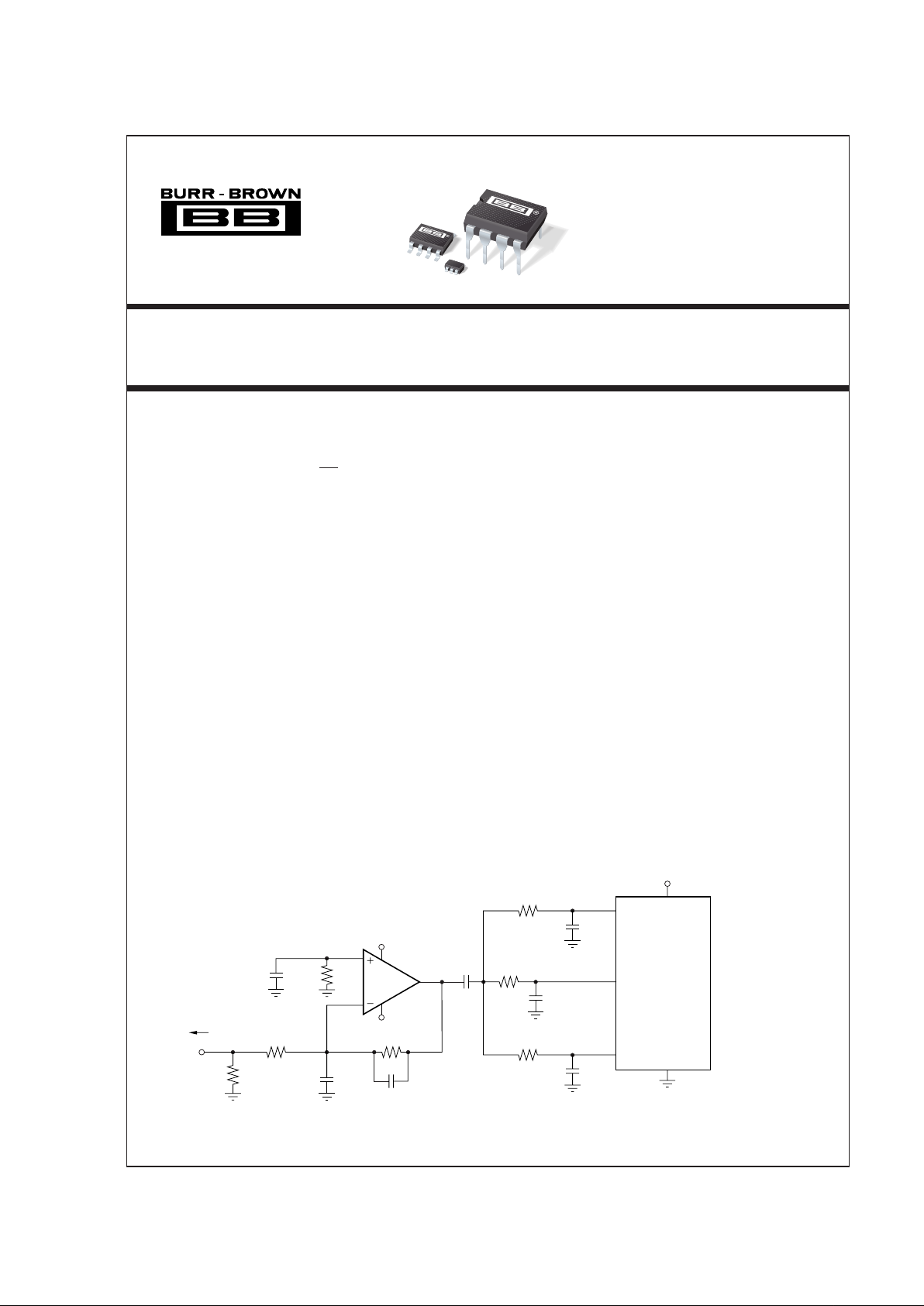
806Ω
50Ω
1Vp-p
10MHz
OPA643
47pF
REFT
+5V
REFB
ADS805
12-Bit
20MSPS
Measured
80dB SFDR
Analog
Input
56.9Ω
0.1µF
0.1µF
402Ω
5kΩ
High Dynamic Range 20MSPS Digitizer
5kΩ
0.1µF
2Vp-p
+5V
–5V
14pF
280Ω
0.1µFLow Gain
Compensation
50Ω
Source
2.7pF
©
1993 Burr-Brown Corporation PDS-1191D Printed in U.S.A. March, 1998
®
OPA643
2
SPECIFICATIONS
ELECTRICAL
At TA = +25°C, VS = ±5V, RL = 100Ω, RF = 402Ω, unless otherwise noted.
OPA643P, U, N OPA643PB, UB, NB
PARAMETER CONDITIONS MIN TYP MAX MIN TYP MAX UNITS
OFFSET VOLTAGE
Input Offset Voltage ±2.5 ±4 ±0.5 ±1.5 mV
Average Drift 53µV/°C
Power Supply Rejection (PSR) V
S
= ±4.5 to ±5.5V 65 90 70 ✻ dB
INPUT BIAS CURRENT
Input Bias Current V
CM
= 0V 19 30 ✻✻ µA
Over Specified Temperature 40 ✻ µA
Input Offset Current V
CM
= 0V 0.1 2.0 ✻✻ µA
Over Specified Temperature 3.0 ✻ µA
NOISE
Input Voltage Noise
Noise Density: f > 1MHz 2.3 ✻ nV/√Hz
Integrated Voltage Noise, BW = 100Hz to 100MHz 23 ✻ µVrms
Input Bias Current Noise
Current Noise Density, f > 1MHz 2.5 ✻ pA/√Hz
INPUT VOLTAGE RANGE
Common-Mode Input Range ±2.75 ±3.0 ✻✻ V
Over Specified Temperature ±2.5 ✻ V
Common-Mode Rejection (CMR) V
CM
= ±0.5V 65 85 80 92 dB
INPUT IMPEDANCE
Differential 7 || 2.5 ✻ kΩ || pF
Common-Mode 630 || 1.3 ✻ kΩ || pF
OPEN-LOOP GAIN
Open-Loop Voltage Gain (A
OL
)V
O
= ±2V, RL = 100Ω 82 95 87 ✻ dB
Over Specified Temperature V
O
= ±2V, RL = 100Ω 80 80 dB
FREQUENCY RESPONSE
Closed-Loop Bandwidth Gain = +5V/V 200 ✻ MHz
Gain = +10V/V 85 ✻ MHz
Gain = +20V/V 40 ✻ MHz
Gain Bandwidth Product (GBP) 800 ✻ MHz
Slew Rate
(1)
G = +5, 2V Step 1000 ✻ V/µs
At Minimum Specified Temperature G = +5, 2V Step 920 ✻ V/µs
Settling Time: 0.01% G = +5, 2V Step 21 ✻ ns
0.1% G = +5, 2V Step 16.5 ✻ ns
1% G = +5, 2V Step 7.5 ns
Spurious Free Dynamic Range (SFDR) G = +5, f = 5MHz 90 95 dBc
V
O
= 2Vp-p, RL = 500Ω
Differential Gain Error at 3.58MHz G = +5V/V, V
O
= 0V to 1.4V, RL = 150Ω 0.005 ✻ %
Differential Phase Error at 3.58MHz G = +5V/V, V
O
= 0V to 1.4V, RL = 150Ω 0.015 ✻ degrees
OUTPUT
Voltage Output No Load ±3.25 ✻ V
Over Specified Temperature ±3.0 ✻ V
Voltage Output, +25°CR
L
= 100Ω±2.75 ✻ V
Over Specified Temperature ±2.5 ✻ V
Current Output, +25°C ±40 ±60 ±50 ±65 mA
Over Specified Temperature ±35 ±40 mA
Closed-Loop Output Resistance 0.1MHz, G = +5V/V 0.055 ✻ Ω
POWER SUPPLY
Specified Operating Voltage ±5 ✻ V
Operating Voltage Range T
MIN
to T
MAX
±4.5 ±5.5 ✻✻V
Quiescent Current ±20 ±25 ±16 ✻✻ mA
Over Specified Temperature ±26 ✻ mA
TEMPERATURE RANGE
Specification: P, U, N Ambient –40 +85 ✻✻°C
Thermal Resistance
θ
JA
, Junction to Ambient
P, PB 8-Pin DIP 100 ✻ °C/W
U, UB 8-Pin SO-8 125 ✻ °C/W
N, NB 5-Pin SOT23-5 150 ✻ °C/W
✻ Specifications same as OPA643P, U, N.
NOTE: (1) Slew rate is rate of change from 10% to 90% of output voltage step.
®
OPA643
3
1
2
3
54+V
S
Inverting Input
Output
–V
S
Non-Inverting Input
1
2
3
4
8
7
6
5
+V
S2
(1)
+V
S1
Output
–V
S2
(1)
NC
Inverting Input
Non-Inverting Input
–V
S1
The information provided herein is believed to be reliable; however, BURR-BROWN assumes no responsibility for inaccuracies or omissions. BURR-BROWN assumes
no responsibility for the use of this information, and all use of such information shall be entirely at the user’s own risk. Prices and specifications are subject to change
without notice. No patent rights or licenses to any of the circuits described herein are implied or granted to any third party. BURR-BROWN does not authorize or warrant
any BURR-BROWN product for use in life support devices and/or systems.
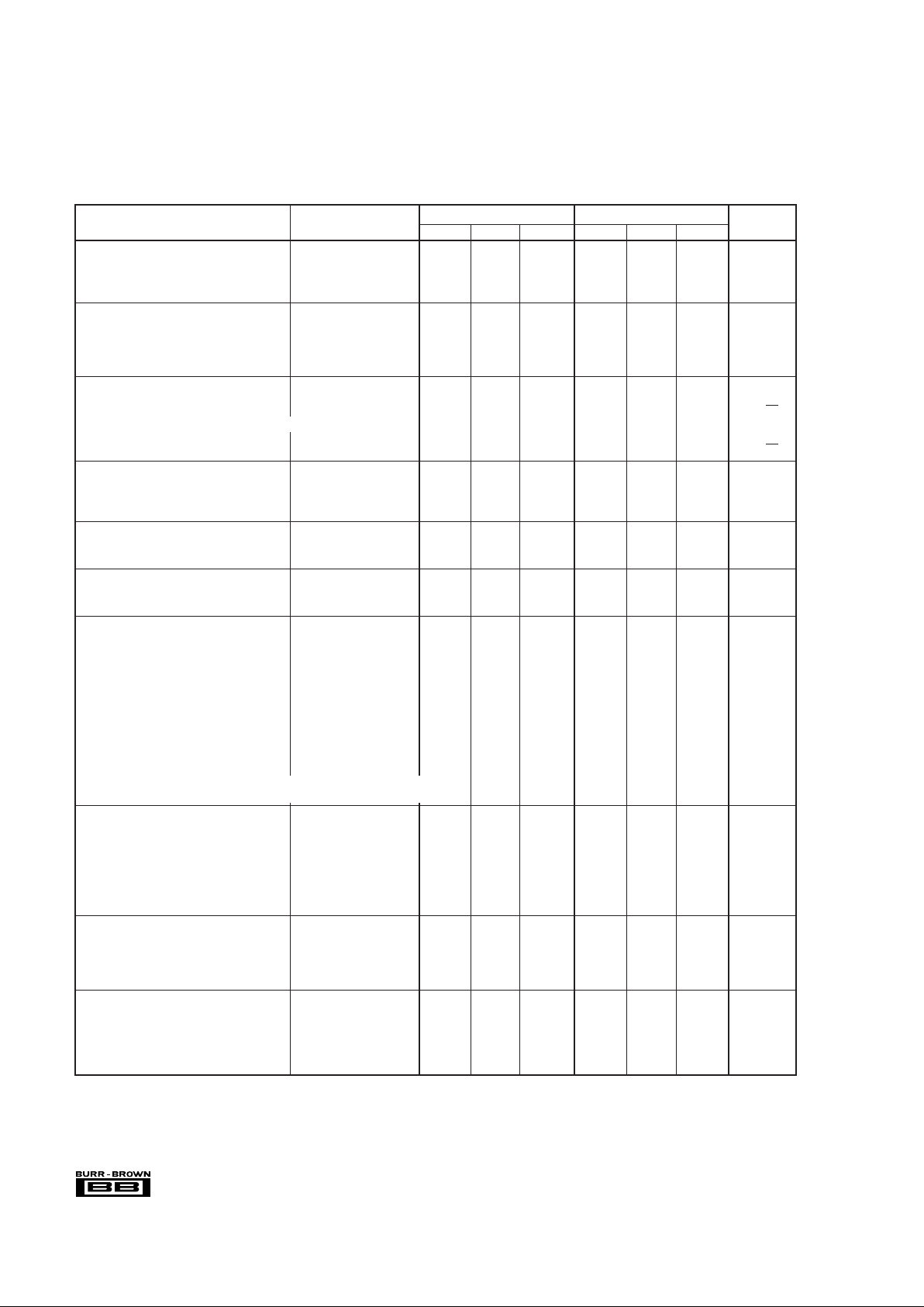
PIN CONFIGURATION
Top View DIP/SO-8
ABSOLUTE MAXIMUM RATINGS
Power Supply (±VS)..................................................................... ±6.0VDC
Internal Power Dissipation
(1)
.................................. See Thermal Analysis
Differential Input Voltage .................................................................. ±1.2V
Input Voltage Range ............................................................................ ±V
S
Storage Temperature Range: P, PB, U, UB, N, NB ..... –40°C to +125°C
Lead Temperature (soldering, 10s).............................................. +300°C
(soldering, SO-8 3s) ....................................... +260°C
Junction Temperature (T
J
) ............................................................ +175°C
NOTE: (1) Packages must be derated based on specified
θ
JA. Maximum T
J
must be observed.
NOTE: (1) Making use of all four power supply pins is highly recommended,
although not required. Using these four pins, instead of just pins 4 and 7, will
lower the power supply impedance improving distortion.
SOT23-5
PACKAGE
DRAWING TEMPERATURE PACKAGE ORDERING
PRODUCT PACKAGE NUMBER
(1)
RANGE MARKING
(2)
NUMBER
(3)
OPA643U SO-8 Surface Mount 182 –40°C to +85°C OPA643U OPA643U
OPA643UB SO-8 Surface Mount 182 –40°C to +85°C OPA643UB OPA643UB
OPA643N 5-pin SOT23-5 331 –40°C to +85°C A43 OPA643N-250
OPA643N-3k
OPA643NB 5-pin SOT23-5 331 –40°C to +85°C A43B OPA643NB-250
OPA643NB-3k
OPA643P 8-Pin Plastic DIP 006 –40°C to +85°C OPA643P OPA643P
OPA643PB 8-Pin Plastic DIP 006 –40°C to +85°C OPA643PB OPA643PB
NOTES: (1) For detailed drawing and dimension table, please see end of data sheet, or Appendix C of Burr-Brown IC Data Book. (2) The “B” grade of the SO-8 and
DIP packages will be marked with a “B” by pin 8. The “B” grade of the SOT23-5 will be marked with a “B” near pins 3 and 4. (3) The SOT23-5 is only available on a 7"
tape and reel (e.g. ordering 250 pieces of “OPA643N-250” will get a single 250 piece tape and reel. Ordering 3000 pieces of “OPA643N-3k” will get a single 3000 piece
tape and reel). Please refer to Appendix B of Burr-Brown IC Data Book for detailed Tape and Reel Mechanical information.
PACKAGE/ORDERING INFORMATION
ELECTROSTATIC
DISCHARGE SENSITIVITY
Electrostatic discharge can cause damage ranging from performance degradation to complete device failure. Burr-Brown
Corporation recommends that all integrated circuits be handled
and stored using appropriate ESD protection methods.
ESD damage can range from subtle performance degradation
to complete device failure. Precision integrated circuits may
be more susceptible to damage because very small parametric
changes could cause the device not to meet published specifications.
®
OPA643
4
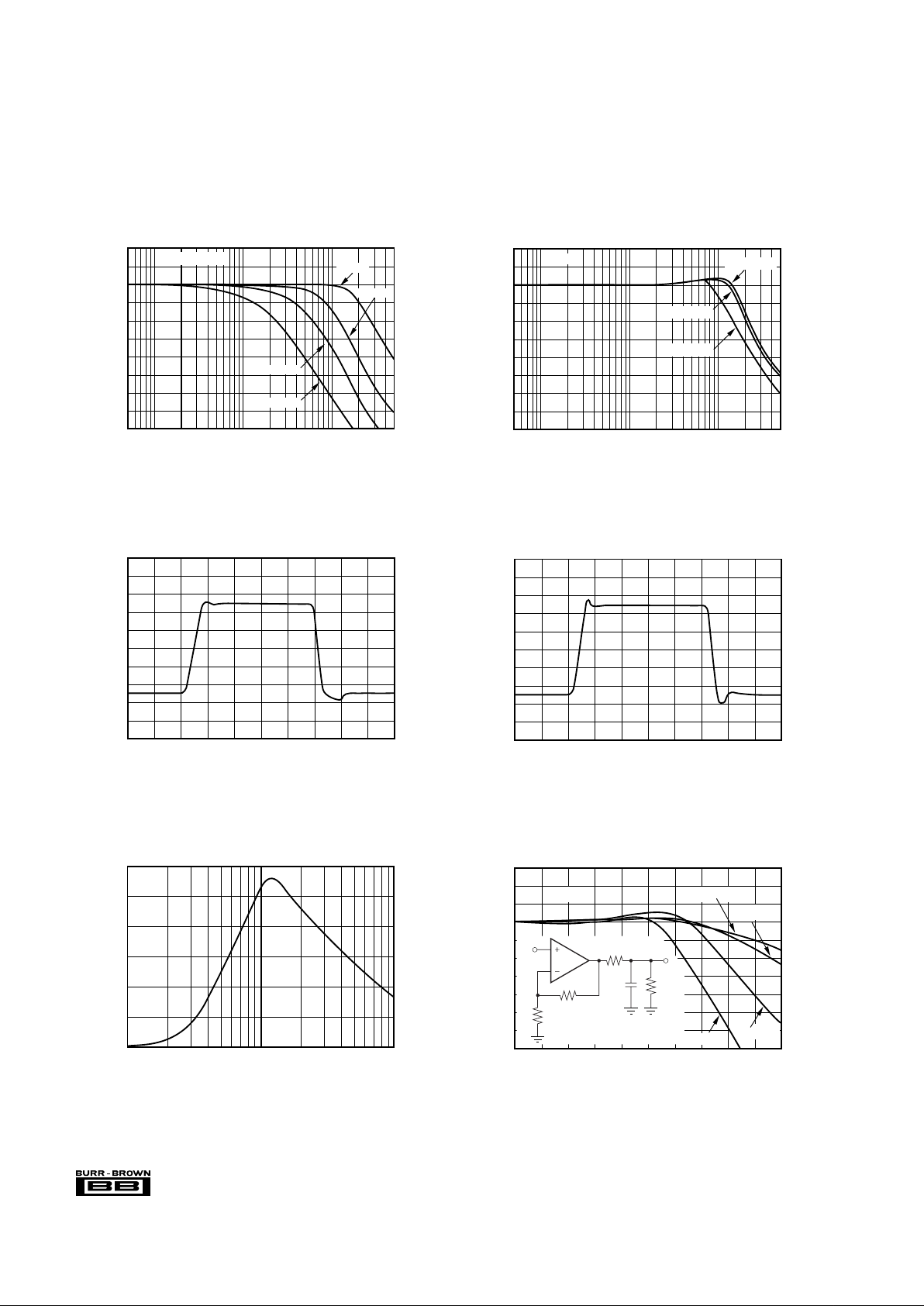
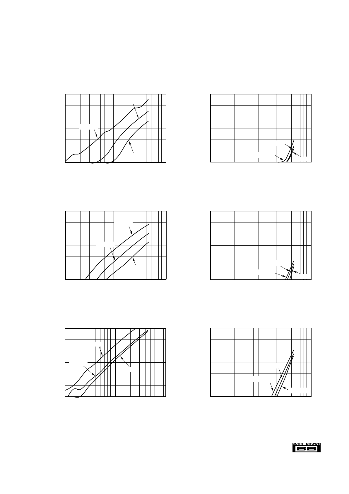
TYPICAL PERFORMANCE CURVES
At TA = +25°C, VS = ±5V, RL = 100Ω, RF = 402Ω, unless otherwise noted
LARGE SIGNAL FREQUENCY RESPONSE
Frequency
0.5MHz 10MHz 100MHz 500MHz
20
17
14
11
8
5
2
–1
–4
–7
–10
Gain (3dB/div)
G = +5
VO = 1Vp-p
VO = 2Vp-p
VO = 4Vp-p
RS vs CAPACITIVE LOAD
Capacitive Load (pF)
101 100
60
50
40
30
20
10
0
R
S
(Ω)
LARGE SIGNAL PULSE RESPONSE
Time (5ns/div)
2.0
1.6
1.2
0.8
0.4
0
–0.4
–0.8
–1.2
–1.4
–2.0
Output Voltage (400mV/div)
SMALL SIGNAL FREQUENCY RESPONSE
Frequency
0.5MHz 10MHz 100MHz 500MHz
6
3
0
–3
–6
–9
–12
–15
–18
–21
–24
Normalized Gain (3dB/div)
VO = 0.1Vp-p
G = +5
G = +10
G = +20
G = +50
FREQUENCY RESPONSE vs CAPACITIVE LOAD
Frequency (20MHz/div)
100MHz0 200MHz
23
20
17
14
11
8
5
2
–1
–4
–7
Gain to Capacitive Load (3dB/div)
CL = 10pFG = +5
CL = 22pF
1kΩ
100Ω
402Ω
(1kΩ is optional)
R
S
C
L
V
IN
V
O
CL = 100pF
CL = 47pF
OPA643
SMALL SIGNAL PULSE RESPONSE
Time (5ns/div)
200
160
120
80
40
0
–40
–80
–120
–160
–200
Output Voltage (40mV/div)
®
OPA643
5
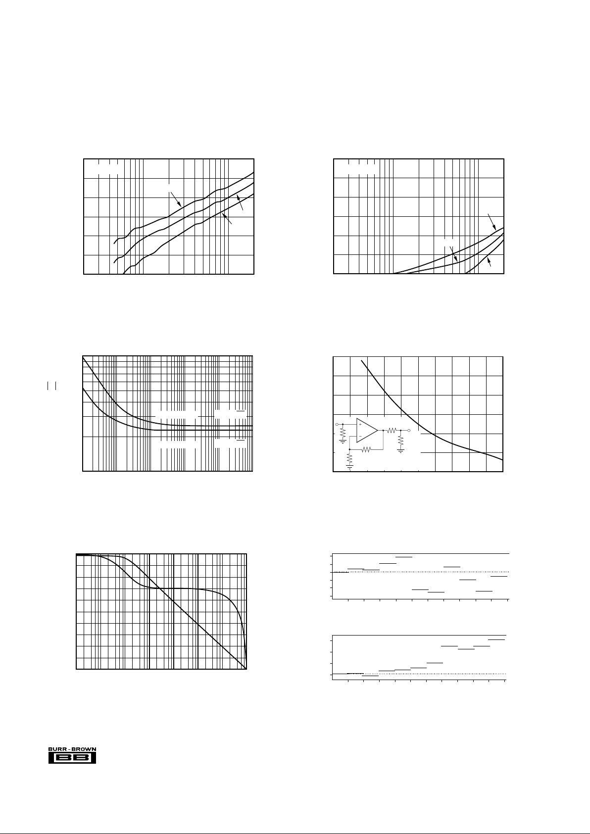
TYPICAL PERFORMANCE CURVES (CONT)
At TA = +25°C, VS = ±5V, RL = 100Ω, RF = 402Ω, unless otherwise noted.
5MHz 2ND HARMONIC DISTORTION
Output Voltage Swing (Vp-p)
10.1 10
G = +5
–70
–75
–80
–85
–90
–95
–100
2nd Harmonic Distortion (dBc)
RL = 500Ω
RL = 100Ω
RL = 200Ω
5MHz 3RD HARMONIC DISTORTION
Output Voltage Swing (Vp-p)
10.1 10
3rd Harmonic Distortion (dBc)
G = +5
–70
–75
–80
–85
–90
–95
–100
RL = 200Ω
RL = 100Ω
RL = 500Ω
10MHz 2ND HARMONIC DISTORTION
Output Voltage Swing (Vp-p)
10.1 10
2nd Harmonic Distortion (dBc)
G = +5
–60
–65
–70
–75
–80
–85
–90
RL = 100Ω
RL = 500Ω
RL = 200Ω
10MHz 3RD HARMONIC DISTORTION
Output Voltage Swing (Vp-p)
10.1 10
G = +5
3rd Harmonic Distortion (dBc)
–60
–65
–70
–75
–80
–85
–90
RL = 500Ω
RL = 100Ω
RL = 200Ω
20MHz 2ND HARMONIC DISTORTION
Output Voltage Swing (Vp-p)
10.1 10
G = +5
2nd Harmonic Distortion (dBc)
–60
–65
–70
–75
–80
–85
–90
RL = 100Ω
RL = 200Ω
RL = 500Ω
20MHz 3RD HARMONIC DISTORTION
Output Voltage Swing (Vp-p)
10.1 10
G = +5
3rd Harmonic Distortion (dBc)
–60
–65
–70
–75
–80
–85
–90
RL = 200Ω
RL = 500Ω
RL = 100Ω
®
OPA643
6
TYPICAL PERFORMANCE CURVES (CONT)
At TA = +25°C, VS = ±5V, RL = 100Ω, RF = 402Ω, unless otherwise noted.
3RD HARMONIC DISTORTION vs FREQUENCY
Frequency (MHz)
1100.1 20
G = 5
–40
–50
–60
–70
–80
–90
–100
3rd Harmonic Distortion (dBc)
VO = 2Vp-p
G = 10
G = 20
0
DC Offset (V)
Differential Gain Error (%)
1.40.7
0
0.7
1.4
DC Offset (V)
Differential Phase Error (°)
0.004
0.002
0.000
–0.002
–0.004
–0.006
0.015
0.010
0.005
0.000
2ND HARMONIC DISTORTION vs FREQUENCY
Frequency (MHz)
1100.1 20
G = 10
–40
–50
–60
–70
–80
–90
–100
2nd Harmonic Distortion (dBc)
VO = 2Vp-p
G = 20
G = 5
OPEN-LOOP GAIN AND PHASE
Frequency (Hz)
10
3
10410510610710810
9
10
2
100
90
80
70
60
50
40
30
20
10
0
Open-Loop Gain (dB)
0
–30
–60
–90
–120
–150
–180
–210
–240
–270
–300
Open-Loop Phase (30°/div)
TWO-TONE, THIRD ORDER
INTERMODULATION INTERCEPT
Frequency (MHz)
50 101520253035404550
55
50
45
40
35
30
25
Intercept (dBm)
100Ω
402Ω
OPA643
50Ω
50Ω
50Ω
P
i
P
O
INPUT VOLTAGE AND CURRENT NOISE DENSITY
Frequency (Hz)
100
10
1
Current Noise pA/√Hz
Voltage Noise nV/√Hz
10
2
10
3
10
4
10
5
10
6
10
7
Current Noise
Voltage Noise
2.5pA/√Hz
2.3nV/√Hz
 Loading...