

Burr Brown OPA640UB, OPA640UB-2K5, OPA640U-2K5, OPA640U Datasheet
®
OPA640
1
FEATURES
● UNITY-GAIN BANDWIDTH: 1.3GHz
● UNITY-GAIN STABLE
● LOW NOISE: 2.9nV/√Hz
● LOW HARMONICS: –75dBc at 10MHz
● HIGH COMMON MODE REJECTION: 85dB
● HIGH SLEW RATE: 350V/µs
OPA640
Wideband Voltage Feedback
OPERATIONAL AMPLIFIER
DESCRIPTION
The OPA640 is an extremely wideband operational
amplifier featuring low noise, high common-mode
rejection and high spurious free dynamic range.
The OPA640 is internally compensated for unity-gain
stability. This amplifier has a fully symmetrical differential input due to its “classical” operational amplifier
circuit architecture. This allows the OPA640 to be used
in all op amp applications requiring high speed and
precision.
Low noise, wide bandwidth, and high linearity make
this amplifier suitable for a variety of RF and video
applications.
®
International Airport Industrial Park • Mailing Address: PO Box 11400, Tucson, AZ 85734 • Street Address: 6730 S. Tucson Blvd., Tucson, AZ 85706 • Tel: (520) 746-1111 • Twx: 910-952-1111
Internet: http://www.burr-brown.com/ • FAXLine: (800) 548-6133 (US/Canada Only) • Cable: BBRCORP • Telex: 066-6491 • FAX: (520) 889-1510 • Immediate Product Info: (800) 548-6132
OPA640
OPA640
APPLICATIONS
● COMMUNICATIONS
● MEDICAL IMAGING
● TEST EQUIPMENT
● CCD IMAGING
● ADC/DAC GAIN AMPLIFIER
● HIGH-RESOLUTION VIDEO
● LOW NOISE PREAMPLIFIER
● DIFFERENTIAL AMPLIFIER
● ACTIVE FILTERS
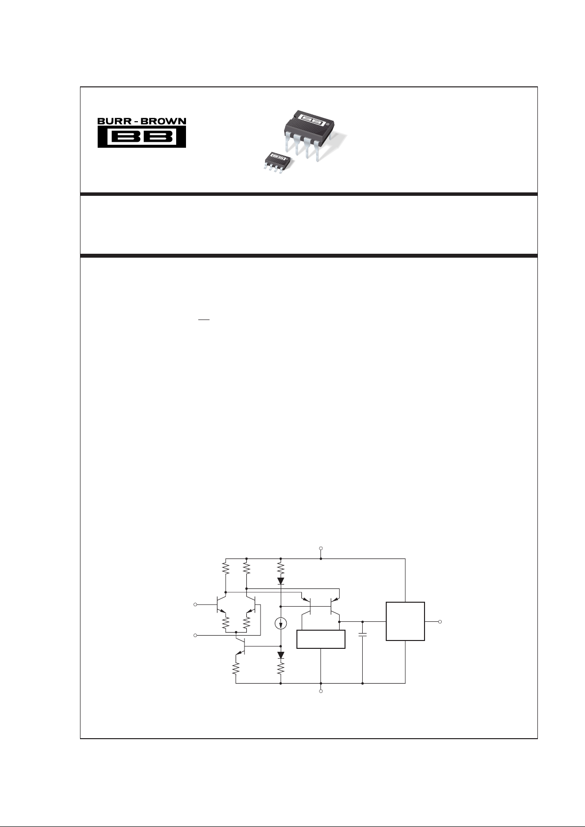
Current
Mirror
Output
Stage
C
C
3
2
Non-Inverting
Input
Inverting
Input
7, 8
+V
S
4, 5
–V
S
6
V
OUT
©
1993 Burr-Brown Corporation PDS-1179D Printed in U.S.A. March, 1998
2OPA640
®
SPECIFICATIONS
ELECTRICAL
At TA = +25°C, VS = ±5V, RL = 100Ω, CL = 2pF, RFB = 402Ω and all four power supply pins are used, unless otherwise noted. RFB = 25Ω for a gain of +1.
OPA640P, U OPA640UB
PARAMETER CONDITIONS MIN TYP MAX MIN TYP MAX UNITS
OFFSET VOLTAGE
Input Offset Voltage ±2.0 ±5 1.0 ±2.0 mV
Average Drift, ±10 ±6 µV/°C
Power Supply Rejection (+V
S
)V
S
= ±4.5 to ±5.5V 60 75 ✻✻ dB
(–V
S
)5360✻✻ dB
INPUT BIAS CURRENT
(1)
Input Bias Current VCM = 0V 15 25 ✻✻ µA
Over Specified Temperature 30 75 18 55 µA
Input Offset Current V
CM
= 0V 0.3 2.0 ✻ 1.0 µA
Over Specified Temperature 0.5 2.5 ✻ 2.0 µA
NOISE
Input Voltage Noise Density
f = 100Hz 7.0 ✻ nV/√Hz
f = 10kHz 2.8 ✻ nV/√Hz
f = 1MHz 2.8 ✻ nV/√Hz
f = 1MHz to 500MHz 2.9 ✻ nV/√Hz
Voltage Noise, BW = 100Hz to 500MHz 65 ✻ µVrms
Input Bias Current Noise Density
f = 0.1Hz to 20kHz 2.0 ✻ pA/√Hz
Noise Figure (NF)
R
S
= 1kΩ 2.6 ✻ dB
R
S
= 50Ω 10.9 ✻ dB
INPUT VOLTAGE RANGE
Common-Mode Input Range ±2.5 ±2.85 ✻✻ V
Over Temperature ±2.5 ±2.75 ✻✻ V
Common-Mode Rejection V
CM
= ±0.5V 70 85 80 88 dB
INPUT IMPEDANCE
Differential 15 || 1 ✻ kΩ || pF
Common-Mode 2 || 1 ✻ MΩ || pF
OPEN-LOOP GAIN, DC
Open-Loop Voltage Gain V
O
= ±2V, RL = 100Ω 50 57 53 ✻ dB
Over Specified Temperature V
O
= ±2V, RL = 100Ω 45 55 ✻✻ dB
FREQUENCY RESPONSE
Closed-Loop Bandwidth Gain = +1V/V 1.3 ✻ GHz
Gain = +2V/V 280 ✻ MHz
Gain = +5V/V 65 ✻ MHz
Gain = +10V/V 31 ✻ MHz
Slew Rate
(2)
G = +1, 2V Step 350 ✻ V/µs
At Minimum Specified Temperature G = +1, 2V Step 285 ✻ V/µs
Settling Time 0.01% G = +1, 2V Step 22 ✻ ns
0.1% G = +1, 2V Step 18 ✻ ns
1% G = +1, 2V Step 4.5 ✻ ns
Spurious Free Dynamic Range G = +1, f = 5MHz, V
O
= 2Vp-p 85 ✻ dBc
G = +1, f = 10MHz, V
O
= 2Vp-p 75 ✻ dBc
G = +1, f = 20MHz, V
O
= 2Vp-p 65 ✻ dBc
Gain Flatness to 0.1dB G = +1 or +2 120 ✻ MHz
Differential Gain at 3.58MHz, V
O
= 0V to 1.4V, RL = 150Ω 0.07 ✻ %
G = +2V/V
Differential Phase at 3.58MHz, V
O
= 0V to 1.4V, RL = 150Ω 0.008 ✻ Degrees
G = +2V/V
OUTPUT
Voltage Output No Load
Over Specified Temperature ±2.6 ±3.0 ✻✻ V
Voltage Output R
L
= 100Ω
Over Specified Temperature ±2.25 ±2.5 ✻✻ V
Current Output, +25°C ±40 ±52 ✻✻ mA
Over Specified Temperature ±25 ±45 ✻✻ mA
Short Circuit Current 75 ✻ mA
Output Resistance 1MHz, G = +1V/V 0.2 ✻ Ω
POWER SUPPLY
Specified Operating Voltage T
MIN
to T
MAX
±5 ✻ V
Operating Voltage Range T
MIN
to T
MAX
±4.5 ±5.5 ✻✻V
Quiescent Current ±18 ±22 ✻✻ mA
Over Specified Temperature ±19 ±24 ✻✻ mA
TEMPERATURE RANGE
Specification: P, U, UB Ambient –40 +85 ✻✻°C
Thermal Resistance
θ
JA
, Junction to Ambient °C/W
P 8-Pin DIP 100 ✻ °C/W
U, UB 8-Pin SO-8 125 ✻ °C/W
NOTE: (1) Slew rate is rate of change from 10% to 90% of output voltage step.
®
OPA640
3
The information provided herein is believed to be reliable; however, BURR-BROWN assumes no responsibility for inaccuracies or omissions. BURR-BROWN assumes
no responsibility for the use of this information, and all use of such information shall be entirely at the user’s own risk. Prices and specifications are subject to change
without notice. No patent rights or licenses to any of the circuits described herein are implied or granted to any third party. BURR-BROWN does not authorize or warrant
any BURR-BROWN product for use in life support devices and/or systems.
ABSOLUTE MAXIMUM RATINGS
Power Supply ..............................................................................±5.5VDC
Internal Power Dissipation .................................. Thermal Considerations
Differential Input Voltage ..................................................................±1.2V
Input Voltage Range ............................................................................ ±V
S
Storage Temperature Range: P, U, UB........................ –40°C to +125°C
Lead Temperature (soldering, 10s).............................................. +300°C
(soldering, SO-8 3s) .......................................+260°C
Junction Temperature (T
J
) ............................................................ +175°C
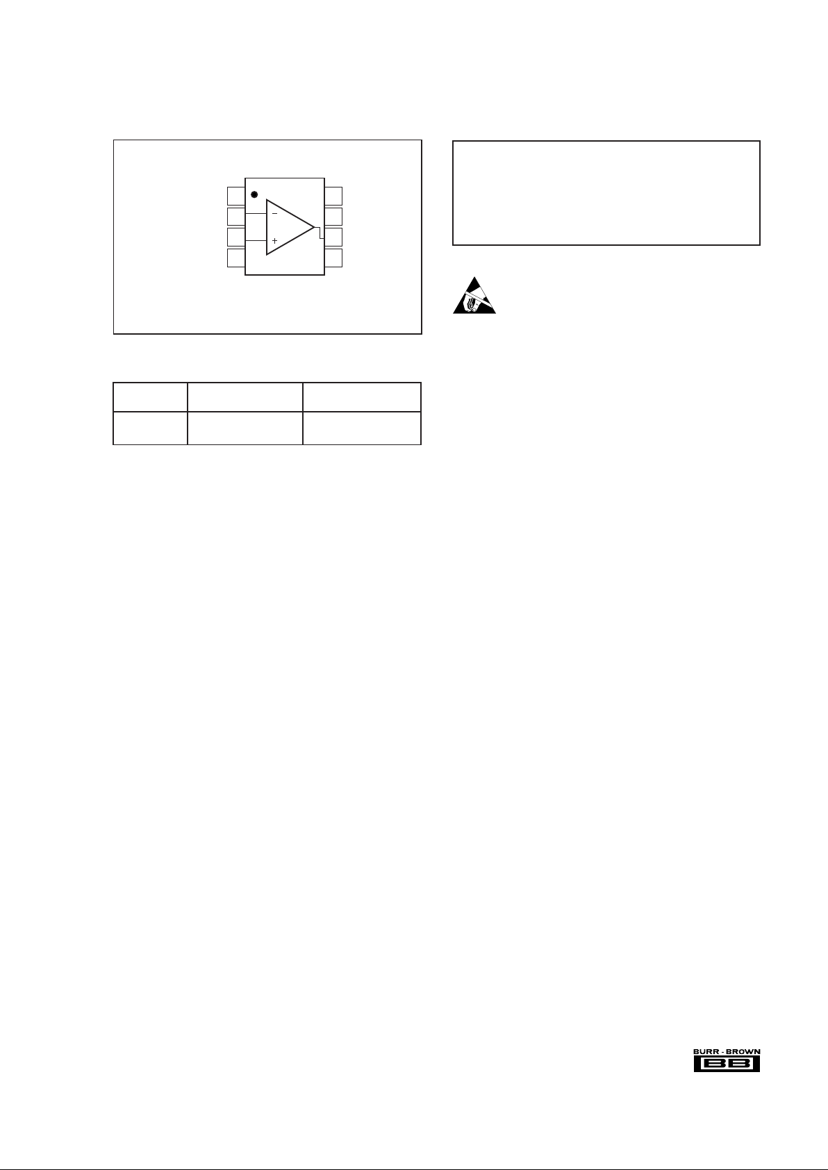
PIN CONFIGURATION
NOTE: (1) Making use of all four power supply pins is highly recommended,
although not required. Using these four pins, instead of just pins 4 and 7, will
lower the effective pin impedance and substantially lower distortion.
Top View DIP/SO-8
ELECTROSTATIC
DISCHARGE SENSITIVITY
Electrostatic discharge can cause damage ranging from performance degradation to complete device failure. BurrBrown Corporation recommends that all integrated circuits
be handled and stored using appropriate ESD protection
methods.
ESD damage can range from subtle performance degradation to complete device failure. Precision integrated circuits
may be more susceptible to damage because very small
parametric changes could cause the device not to meet
published specifications.
PACKAGE DRAWING
PRODUCT PACKAGE NUMBER
(1)
OPA640P 8-Pin Plastic DIP 006
OPA640U, UB SO-8 Surface Mount 182
NOTE: (1) For detailed drawing and dimension table, please see end of data
sheet, or Appendix C of Burr-Brown IC Data Book. (2) The “B” grade of the
SO-8 and package will be marked with a “B” by pin 8.
PACKAGE/ORDERING INFORMATION
1
2
3
4
8
7
6
5
+V
S2
(1)
+V
S1
Output
–V
S2
(1)
NC
Inverting Input
Non-Inverting Input
–V
S1
4OPA640
®
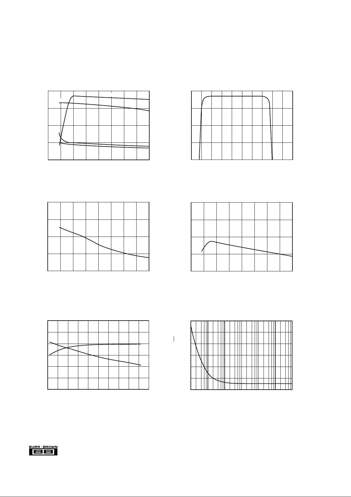
TYPICAL PERFORMANCE CURVES
TA = +25°C, VS = ±5V, RL = 100Ω, CL = 2pF, RFB = 402Ω and all four power supply pins are used, unless otherwise noted. RFB = 25Ω for a gain of +1.
90
80
70
60
50
–75
Temperature (°C)
A
OL
, PSR, CMR (dB)
AOL, PSR, AND CMR vs TEMPERATURE
–50 –25 0 25 50 75 100 125
–PSR
A
OL
+PSR
CMR
90
85
80
75
70
–5
Common-Mode Voltage (V)
Common-Mode Rejection (dB)
COMMON-MODE REJECTION
vs INPUT COMMON-MODE VOLTAGE
–4 –3 –2 –1 0 1 2 3 4 5
26
22
18
14
10
–75
Ambient Temperature (°C)
Input Bias Current (µA)
INPUT BIAS CURRENT vs TEMPERATURE
–50 –25 0 25 50 75 100 125
20
19
18
17
16
–75
Ambient Temperature (°C)
Supply Current (±mA)
SUPPLY CURRENT vs TEMPERATURE
–50 –25 0 25 50 75 100 125
70
60
50
40
–60
Ambient Temperature (°C)
Output Current (±mA)
OUTPUT CURRENT vs TEMPERATURE
–40 –20 0 20 40 60 80 100 120 140
–I
O
+I
O
30
25
20
15
10
5
0
VOLTAGE NOISE vs FREQUENCY
Voltage Noise (nV/√Hz)
Frequency (Hz)
100 1k 10k 100k 1M 10M10
 Loading...