

Burr Brown OPA620KP, OPA620KU, OPA620KU-2K5 Datasheet
©
1988 Burr-Brown Corporation PDS-872G Printed in U.S.A. September, 1993
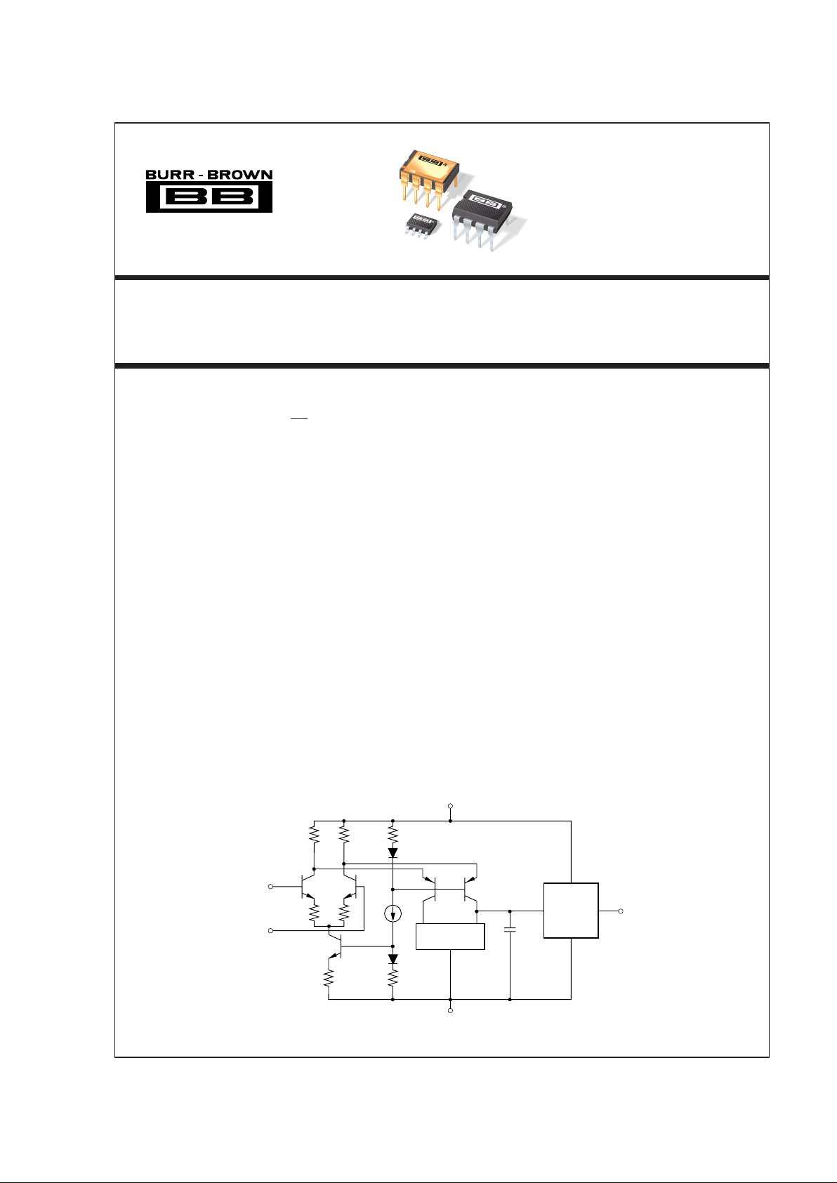
DESCRIPTION
The OPA620 is a precision wideband monolithic operational amplifier featuring very fast settling time, low
differential gain and phase error, and high output
current drive capability.
The OPA620 is internally compensated for unity-gain
stability. This amplifier has a very low offset, fully
symmetrical differential input due to its “classical”
operational amplifier circuit architecture. Unlike “current-feedback” amplifier designs, the OPA620 may be
OPA620
Current
Mirror
Output
Stage
C
C
3
2
Non-Inverting
Input
Inverting
Input
7
+V
CC
4
–V
CC
6
Output
®
used in all op amp applications requiring high speed
and precision.
Low noise and distortion, wide bandwidth, and high
linearity make this amplifier suitable for RF and video
applications. Short-circuit protection is provided by an
internal current-limiting circuit.
The OPA620 is available in plastic and ceramic DIP
and SO-8 packages. Two temperature ranges are offered: –40°C to +85°C and –55°C to +125°C.
APPLICATIONS
● LOW NOISE PREAMPLIFIER
● LOW NOISE DIFFERENTIAL AMPLIFIER
● HIGH-RESOLUTION VIDEO
● HIGH-SPEED SIGNAL PROCESSING
● LINE DRIVER
● ADC/DAC BUFFER
● ULTRASOUND
● PULSE/RF AMPLIFIERS
● ACTIVE FILTERS
Wideband Precision
OPERATIONAL AMPLIFIER
FEATURES
● LOW NOISE: 2.3nV/√Hz
● HIGH OUTPUT CURRENT: 100mA
● FAST SETTLING: 25ns (0.01%)
● GAIN-BANDWIDTH PRODUCT: 200MHz
● UNITY-GAIN STABLE
● LOW OFFSET VOLTAGE:
±200µV
● LOW DIFFERENTIAL GAIN/PHASE ERROR
● 8-PIN DIP, SO-8 PACKAGES
International Airport Industrial Park • Mailing Address: PO Box 11400, Tucson, AZ 85734 • Street Address: 6730 S. Tucson Blvd., Tucson, AZ 85706 • Tel: (520) 746-1111 • Twx: 910-952-1111
Internet: http://www.burr-brown.com/ • FAXLine: (800) 548-6133 (US/Canada Only) • Cable: BBRCORP • Telex: 066-6491 • FAX: (520) 889-1510 • Immediate Product Info: (800) 548-6132
OPA620
OPA620
OPA620
®
OPA620
2
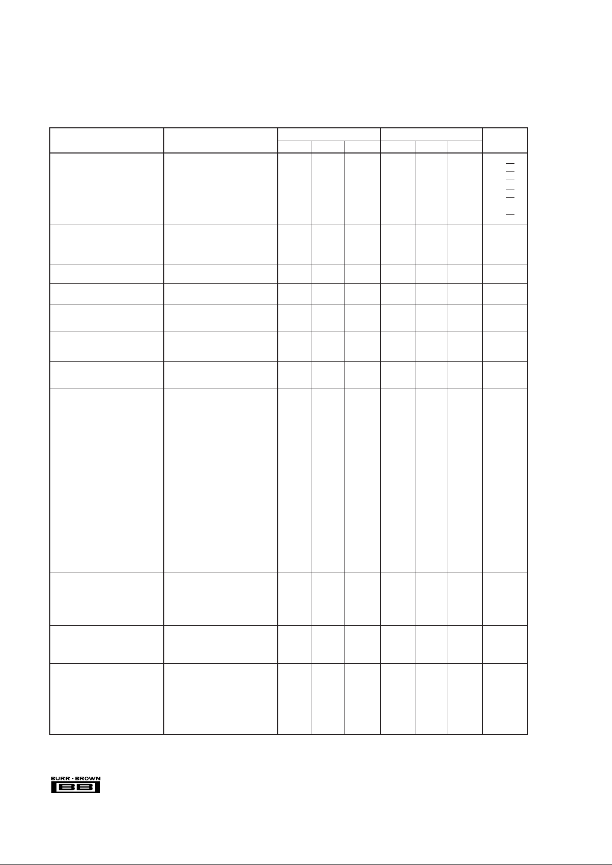
OPA620KP, KU OPA620SG
PARAMETER CONDITIONS MIN TYP MAX MIN TYP MAX UNITS
INPUT NOISE
Voltage: f
O
= 100Hz RS = 0Ω 10 ✻ nV/√Hz
f
O
= 1kHz 5.5 ✻ nV/√Hz
f
O
= 10kHz 3.3 ✻ nV/√Hz
f
O
= 100kHz 2.5 ✻ nV/√Hz
f
O
= 1MHz to 100MHz 2.3 ✻ nV/√Hz
f
B
= 100Hz to 10MHz 8.0 ✻ µVrms
Current: f
O
= 10kHz to 100MHz 2.3 ✻ pA/√Hz
OFFSET VOLTAGE
(1)
Input Offset Voltage VCM = 0VDC ±200 ±1000 ✻✻ µV
Average Drift T
A
= T
MIN
to T
MAX
±8 ✻ µV/°C
Supply Rejection ±V
CC
= 4.5V to 5.5V 50 60 ✻✻ dB
BIAS CURRENT
Input Bias Current V
CM
= 0VDC 15 30 ✻✻ µA
OFFSET CURRENT
Input Offset Current V
CM
= 0VDC 0.2 2 ✻✻ µA
INPUT IMPEDANCE
Differential Open-Loop 15 ||
1 ✻ kΩ || pF
Common-Mode 1 ||
1 ✻ MΩ || pF
INPUT VOLTAGE RANGE
Common-Mode Input Range ±3.0 ±3.5 ✻✻ V
Common-Mode Rejection V
IN
= ±2.5VDC, VO = 0VDC 65 75 ✻✻ dB
OPEN-LOOP GAIN, DC
Open-Loop Voltage Gain R
L
= 100Ω 50 60 ✻✻ dB
R
L
= 50Ω 48 58 ✻✻ dB
FREQUENCY RESPONSE
Closed-Loop Bandwidth Gain = +1V/V 300 ✻ MHz
(–3dB) Gain = +2V/V 100 ✻ MHz
Gain = +5V/V 40 ✻ MHz
Gain = +10V/V 20 ✻ MHz
Gain-Bandwidth Product Gain ≥ +5V/V 200 ✻ MHz
Differential Gain 3.58MHz, G = +1V/V 0.05 ✻ %
Differential Phase 3.58MHz, G = +1V/V 0.05 ✻ Degrees
Harmonic Distortion
(2)
G = +2V/V, f = 10MHz, VO = 2Vp-p
Second Harmonic –61 –50 ✻✻dBc
(3)
Third Harmonic –65 –55 ✻✻ dBc
Full Power Bandwidth
(2)
VO = 5Vp-p, Gain = +1V/V 11 16 ✻✻ MHz
V
O
= 2Vp-p, Gain = +1V/V 27 40 ✻✻ MHz
Slew Rate
(2)
2V Step, Gain = –1V/V 175 250 ✻✻ V/µs
Overshoot 2V Step, Gain = –1V/V 10 ✻ %
Settling Time: 0.1% 2V Step, Gain = –1V/V 13 ✻ ns
0.01% 25 ✻ ns
Phase Margin Gain = +1V/V 60 ✻ Degrees
Rise Time Gain = +1V/V, 10% to 90%
V
O
= 100mVp-p; Small Signal 2 ✻ ns
V
O
= 6Vp-p; Large Signal 22 ✻ ns
RATED OUTPUT
Voltage Output R
L
= 100Ω±3.0 ±3.5 ✻✻ V
R
L
= 50Ω±2.5 ±3.0 ✻✻ V
Output Resistance 1MHz, Gain = +1V/V 0.015 ✻ Ω
Load Capacitance Stability Gain = +1V/V 20 ✻ pF
Short Circuit Current Continuous ±150 ✻ mA
POWER SUPPLY
Rated Voltage ±V
CC
5 ✻ VDC
Derated Performance ±V
CC
4.0 6.0 ✻✻VDC
Current, Quiescent I
O
= 0mA 21 23 ✻✻ mA
TEMPERATURE RANGE
Specification: KP, KU Ambient Temperature –40 +85 ✻✻°C
SG –55 +125 °C
Operating: SG Ambient Temperature –55 +125 °C
KP, KU –40 +85 °C
θ
JA
:SG 125 °C/W
KP 90 °C/W
KU 100 °C/W
ELECTRICAL
At VCC = ±5VDC, RL = 100Ω, and TA = +25°C, unless otherwise noted.
SPECIFICATIONS
The information provided herein is believed to be reliable; however, BURR-BROWN assumes no responsibility for inaccuracies or omissions. BURR-BROWN assumes no responsibility
for the use of this information, and all use of such information shall be entirely at the user’s own risk. Prices and specifications are subject to change without notice. No patent rights or
licenses to any of the circuits described herein are implied or granted to any third party. BURR-BROWN does not authorize or warrant any BURR-BROWN product for use in life support
devices and/or systems.
3
®
OPA620
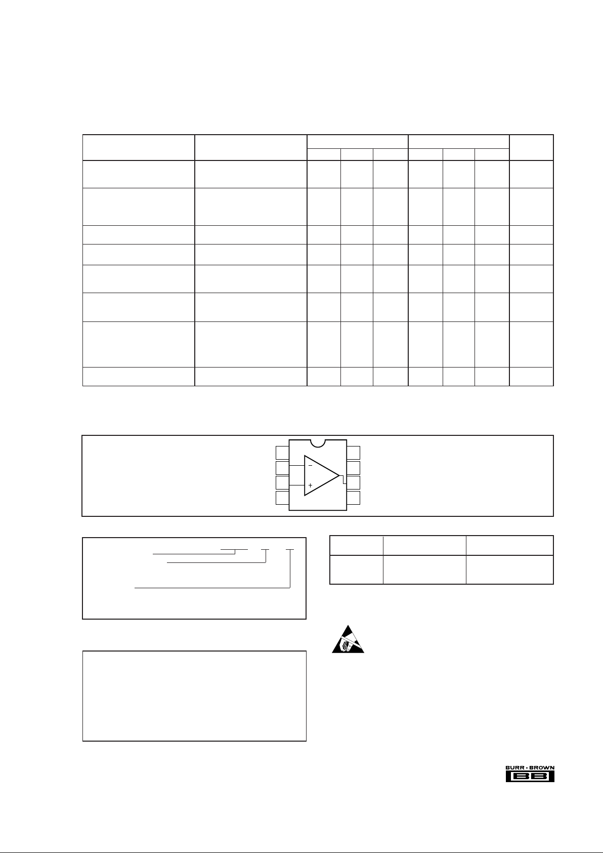
SPECIFICATIONS (CONT)
ELECTRICAL (FULL TEMPERATURE RANGE SPECIFICATIONS)
At VCC = ±5VDC, RL = 100Ω, and TA = T
MIN
to T
MAX
, unless otherwise noted.
TEMPERATURE RANGE
Specification: KP, KU Ambient Temperature –40 +85 ✻✻°C
SG –55 +125 °C
OFFSET VOLTAGE
(1)
Average Drift Full Temp. ±8 ✻ µV/°C
Supply Rejection 0°C to +70°C ±V
CC
= 4.5V to 5.5V 45 60 ✻✻ dB
Full Temp., ±V
CC
= 4.5 to 5.5V 40 55 ✻✻ dB
BIAS CURRENT
Input Bias Current Full Temp., V
CM
= 0VDC 15 40 ✻✻ µA
OFFSET CURRENT
Input Offset Current Full Temp., V
CM
= 0VDC 0.2 5 ✻✻ µA
INPUT VOLTAGE RANGE
Common-Mode Input Range ±2.5 ±3.0 ✻✻ V
Common-Mode Rejection V
IN
= ±2.5VDC, VO = 0VDC 60 75 ✻✻ dB
OPEN LOOP GAIN, DC
Open-Loop Voltage Gain R
L
= 100Ω 46 60 ✻✻ dB
R
L
= 50Ω 44 58 ✻✻ dB
RATED OUTPUT
Voltage Output 0°C to +70°C, R
L
= 100Ω±3.0 ±3.5 ✻✻ V
–40°C to +85°C, R
L
= 100Ω±2.75 ±3.25 ✻✻ V
0°C to +70°C, R
L
= 50Ω±2.5 ±3.0 ✻✻ V
–40°C to +85°C, R
L
= 50Ω±2.25 ±2.7 ✻✻ V
POWER SUPPLY
Current, Quiescent I
O
= 0mA 21 25 ✻✻ mA
OPA620KP, KU OPA620SG
PARAMETER CONDITIONS MIN TYP MAX MIN TYP MAX UNITS
✻ Same specifications as for KP, KU.
NOTES: (1) Offset Voltage specifications are also guaranteed with units fully warmed up. (2) Parameter is guaranteed by characterization. (3) dBc = dB referred
to carrier-input signal.
PIN CONFIGURATION
Top View
DIP/SO-8
1
2
3
4
8
7
6
5
No Internal Connection
Positive Supply (+V )
Output
No Internal Connection
No Internal Connection
Inverting Input
Non-Inverting Input
Negative Supply (–V )
CC
CC
OPA620
Basic Model Number
Performance Grade Code
K = –40°C to +85°C
S = –55°C to +125°C
Package Code
G = 8-pin Ceramic DIP
P = 8-pin Plastic DIP
U = SO-8 Surface Mount
ORDERING INFORMATION
()
()
ABSOLUTE MAXIMUM RATINGS
Supply .............................................................................................±7VDC
Internal Power Dissipation
(1)
.......................See Applications Information
Differential Input Voltage ............................................................ Total V
CC
Input Voltage Range .................................... See Applications Information
Storage Temperature Range: SG ................................. –65°C to +150°C
KP, KU .......................... –40°C to +125°C
Lead Temperature (soldering, 10s).............................................. +300°C
(soldering, SO-8, 3s) ...................................... +260°C
Output Short Circuit to Ground (+25°C) ............... Continuous to Ground
Junction Temperature (T
J
) ............................................................ +175°C
NOTE: (1) Packages must be derated based on specified
θ
JA. Maximum T
J
must be observed.
PACKAGE INFORMATION
PACKAGE DRAWING
PRODUCT PACKAGE NUMBER
(1)
OPA620KP 8-Pin Plastic DIP 006
OPA620KU SO-8 Surface Mount 182
OPA620SG 8-Pin Ceramic DIP 157
NOTE: (1) For detailed drawing and dimension table, please see end of data
sheet, or Appendix C of Burr-Brown IC Data Book.
ELECTROSTATIC
DISCHARGE SENSITIVITY
This integrated circuit can be damaged by ESD. Burr-Brown
recommends that all integrated circuits be handled with
appropriate precautions. Failure to observe proper handling and
installation procedures can cause damage.
ESD damage can range from subtle performance degradation to
complete device failure. Precision integrated circuits may be more
susceptible to damage because very small parametric changes
could cause the device not to meet its published specifications.
®
OPA620
4
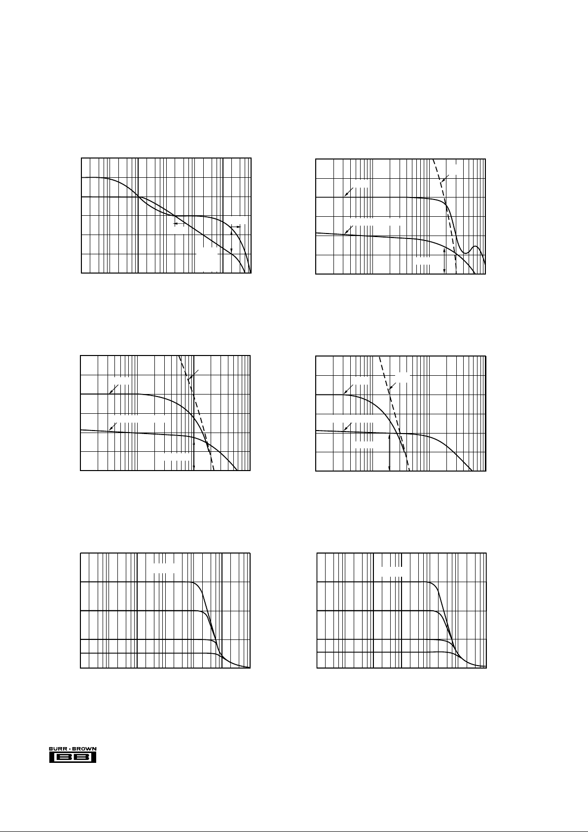
TYPICAL PERFORMANCE CURVES (CONT)
At VCC = ±5VDC, RL = 100Ω, and TA = +25°C, unless otherwise noted.
OPEN-LOOP FREQUENCY RESPONSE
Frequency (Hz)
1k 10k 100k 1M 10M 100M 1G
80
60
40
20
0
-20
Open-Loop Voltage Gain (dB)
Gain
Phase
Phase
Margin
60°
≈
0
–45
–90
–135
–180
Phase Shift (°)
A = +1V/V CLOSED-LOOP
SMALL-SIGNAL BANDWIDTH
V
Frequency (Hz)
+4
+2
0
–4
–6
–8
1M 10M 100M 1G
0
–45
–90
–135
–180
Gain (dB)
–2
Phase Shift (°)
A
OL
PM 60°
Gain
Open-Loop Phase
≈
A = +2V/V CLOSED-LOOP
SMALL-SIGNAL BANDWIDTH
V
Frequency (Hz)
+10
+8
+6
+2
0
–2
1M 10M 100M 1G
0
–45
–90
–135
–180
Gain (dB)
+4
Phase Shift (°)
A
OL
PM 70°
Gain
Open-Loop Phase
≈
AV = +10V/V CLOSED-LOOP
SMALL-SIGNAL BANDWIDTH
Frequency (Hz)
+24
+22
+20
+16
+14
+12
1M 10M 100M 1G
0
–45
–90
–135
–180
Gain (dB)
+18
Phase Shift (°)
OL
Gain
Open-Loop Phase
A
PM 90°
≈
A = +1V/V CLOSED-LOOP BANDWIDTH
vs OUTPUT VOLTAGE SWING
V
Frequency (Hz)
8
6
0
1M 10M 100M 1G
Output Voltage (Vp-p)
4
1k 10k 100k
2
Ω
R = 50
L
A = +2V/V CLOSED-LOOP BANDWIDTH
vs OUTPUT VOLTAGE SWING
V
Frequency (Hz)
8
6
0
1M 10M 100M 1G
Output Voltage (Vp-p)
4
1k 10k 100k
2
Ω
R = 50
L
5
®
OPA620
TYPICAL PERFORMANCE CURVES (CONT)
At VCC = ±5VDC, RL = 100Ω, and TA = +25°C, unless otherwise noted.
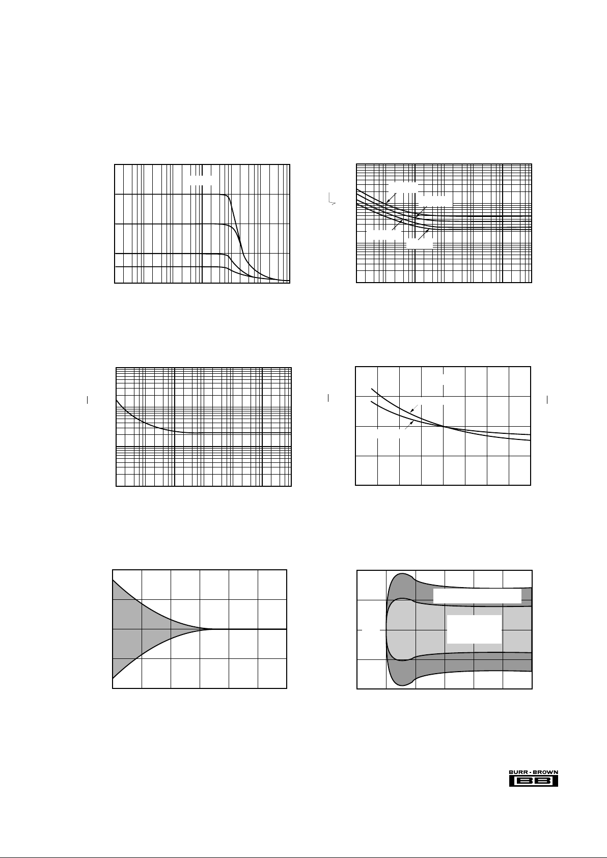
61
INPUT OFFSET VOLTAGE WARM-UP DRIFT
+100
+50
0
–50
–100
02345
Offset Voltage Change (µV)
Time from Power Turn-on (min)
INPUT VOLTAGE AND CURRENT NOISE
SPECTRAL DENSITY vs TEMPERATURE
3.1
2.8
2.5
2.2
1.9
–75 –50 –25 0 +25 +50 +75 +100 +125
2.9
2.6
2.3
2.0
1.7
Voltage Noise (nV/√Hz)
Current Noise (pA/√Hz)
Ambient Temperature (°C)
f = 100kHz
O
Current Noise
Voltage Noise
TOTAL INPUT VOLTAGE NOISE SPECTRAL DENSITY
vs SOURCE RESISTANCE
Frequency (Hz)
100
0.1
1M 10M 100M
Voltage Noise (nV/ Hz)
10
100 1k 10k1100k
Ω
R = 1k
S
ΩR = 500
S
Ω
S
ΩR = 0
S
R = 100
A = +10V/V CLOSED-LOOP BANDWIDTH
vs OUTPUT VOLTAGE SWING
V
Frequency (Hz)
8
6
0
1M 10M 100M 1G
Output Voltage (Vp-p)
4
1k 10k 100k
2
Ω
R = 50
L
INPUT CURRENT NOISE SPECTRAL DENSITY
Frequency (Hz)
100
0.1
1M 10M 100M
10
100 1k 10k
1
100k
Current Noise (pA/√Hz)
0
INPUT OFFSET VOLTAGE CHANGE
DUE TO THERMAL SHOCK
+1000
+500
0
–500
–1000
–1 +1
+2
+3 +4
Offset Voltage Change (µV)
Time from Thermal Shock (min)
+5
K Grade
T = 25°C to 70°C
Air Environment
A
SG T = 25°C to T = 125°C
Air Environment
AA
25°C
 Loading...