

Burr Brown OPA603AU-1K, OPA603AU, OPA603AP Datasheet
©
1989 Burr-Brown Corporation PDS-1026E Printed in U.S.A. February, 1995
International Airport Industrial Park • Mailing Address: PO Box 11400, Tucson, AZ 85734 • Street Address: 6730 S. Tucson Blvd., Tucson, AZ 85706 • Tel: (520) 746-1111 • Twx: 910-952-1111
Internet: http://www.burr-brown.com/ • FAXLine: (800) 548-6133 (US/Canada Only) • Cable: BBRCORP • Telex: 066-6491 • FAX: (520) 889-1510 • Immediate Product Info: (800) 548-6132
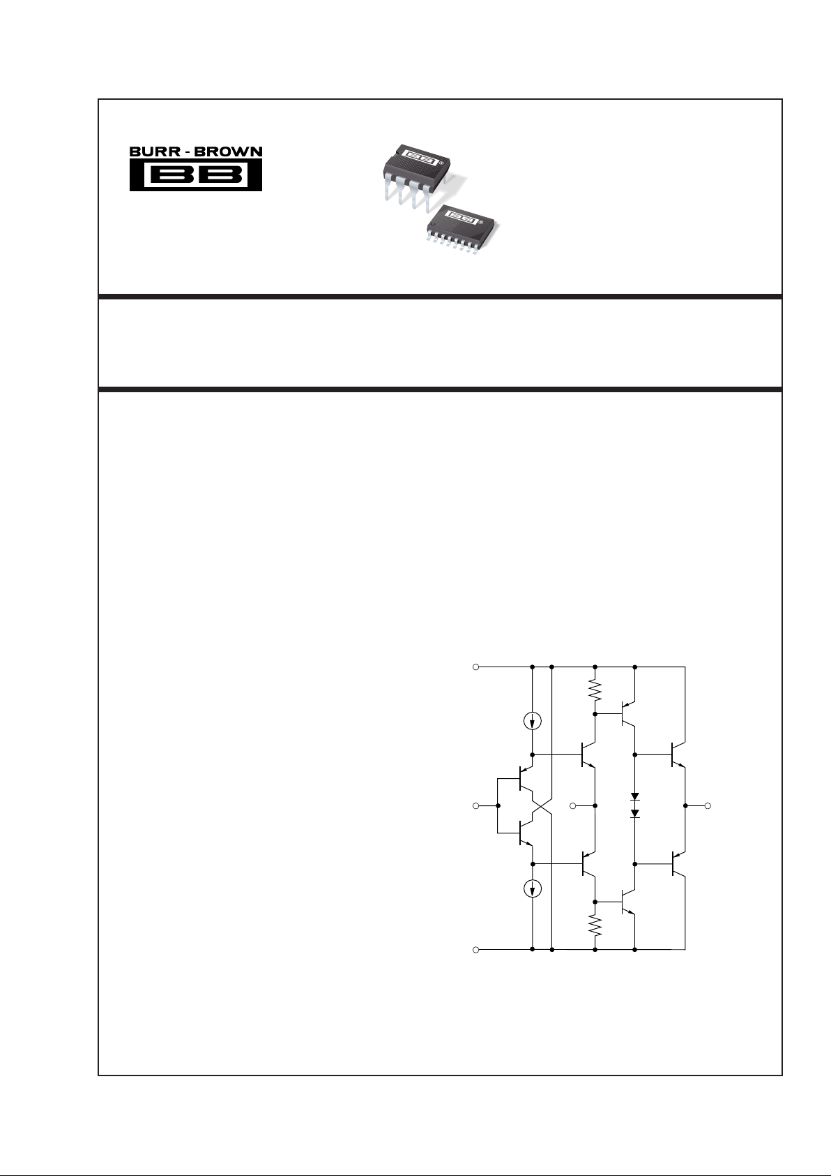
High Speed, Current-Feedback, High Voltage
OPERATIONAL AMPLIFIER
FEATURES
● WIDE SUPPLY RANGE: ±4.5 to ±18V
● BANDWIDTH: 100MHz, G = 1 to 10
● SLEW RATE: 1000V/µs
● FAST SETTLING TIME: 50ns to 0.1%
● HIGH OUTPUT CURRENT: ±150mA peak
● HIGH OUTPUT VOLTAGE: ±12V
DESCRIPTION
The OPA603 is a high-speed current-feedback op amp
with guaranteed specifications at both ±5V and ±15V
power supplies. It can deliver full ±10V signals into
150Ω loads with up to 1000V/µs slew rate. This
allows it to drive terminated 75Ω cables. With 150mA
peak output current capability it is suitable for driving
load capacitance or long lines at high speed.
In contrast with conventional op amps, the currentfeedback approach provides nearly constant bandwidth and settling time over a wide range of closedloop voltage gains.
The OPA603 is available in a plastic 8-pin DIP and
SO-16 surface-mount packages, specified over the
industrial temperature range.
APPLICATIONS
● VIDEO AMPLIFIER
● PULSE AMPLIFIER
● SONAR, ULTRASOUND BUFFERS
● ATE PIN DRIVERS
● xDSL LINE DRIVER
● FAST DATA ACQUISTION
● WAVEFORM GENERATORS
–V
S
4
+In
3
+V
S
7
V
O
6
–In
2
®
OPA603
OPA603
OPA603

®
OPA603
2
OPA603AP, AU
PARAMETER CONDITIONS MIN TYP MAX UNITS
INPUT OFFSET VOLTAGE
Initial 5mV
vs Temperature 8 µV/°C
vs Common-Mode Voltage V
CM
= ±10V 50 60 dB
vs Supply (tracking) Voltage V
S
= ±12V to ±18V 80 85 dB
vs Supply (non-tracking)
(1)
|VS| = 12V to 18V 55 60 dB
+INPUT BIAS CURRENT
Initial 5 µA
vs Temperature 30 nA/°C
vs Common-Mode V
CM
= ±10V 200 500 nA/V
vs Supply (tracking) V
S
= ±12V to ±18V 50 100 nA/V
vs Supply (non-tracking)
(1)
|VS| = 12V to 18V 150 300 nA/V
–INPUT BIAS CURRENT
Initial 25 µA
vs Temperature 300 nA/°C
vs Common-Mode V
CM
= ±10V 200 600 nA/V
vs Supply (tracking) V
S
= ±12V to ±18V 300 500 nA/V
vs Supply (non-tracking)
(1)
|VS| = 12V to 18V 1500 2000 nA/V
INPUT IMPEDANCE
+Input 5 || 2 MΩ || pF
–Input 30 || 2 Ω || pF
OPEN LOOP CHARACTERISTICS
Transresistance V
O
= ±10V 300 440 kΩ
Transcapacitance 1.8 pF
OUTPUT CHARACTERISTICS
Voltage R
L
= 150Ω ±10 ±12 V
Peak Current 150 mA
Short-Circuit Current
(2)
VO = 0V 250 mA
Output Resistance, Open-Loop 70 Ω
FREQUENCY RESPONSE G
= +2
Small-Signal Bandwidth
(3)
70 160 MHz
Gain Flatness, ±0.5dB 35 75 MHz
Full-Power Bandwidth V
O
= 20Vp-p 10 MHz
Differential Gain f = 4.43MHz, V
O
= 1V 0.03 %
Differential Phase f = 4.43MHz, V
O
= 1V 0.025 Degrees
TIME DOMAIN RESPONSE G
= +2
Propagation Delay 10 ns
Rise and Fall Time 10 ns
Settling Time to 0.10% 10V Step 50 ns
Slew Rate 1000 V/µs
DISTORTION G
= +2, RL = 100Ω, f = 10MHz
2nd Harmonic Distortion V
O
= 0.2Vp-p –60 –65 dBc
3rd Harmonic Distortion V
O
= 0.2Vp-p –70 –90 dBc
POWER SUPPLY
Specified Operating Voltage ±15 V
Operating Voltage Range ±4.5 ±18 V
Current ±21 ±25 mA
TEMPERATURE RANGE
Specification –25 +85 °C
Storage –40 +150 °C
THERMAL RESISTANCE,
θ
JA
Soldered to Printed Circuit 90 °C/W
SPECIFICATIONS: V
S
= ±15V
ELECTRICAL
At TA = +25°C, and RL = 150Ω, unless otherwise noted.
NOTES: (1) One power supply fixed at 15V; the other supply varied from 12V to 18V. (2) Observe power derating curve. (3) See bandwidth versus gain curve,
Figure 5.
The information provided herein is believed to be reliable; however, BURR-BROWN assumes no responsibility for inaccuracies or omissions. BURR-BROWN assumes
no responsibility for the use of this information, and all use of such information shall be entirely at the user’s own risk. Prices and specifications are subject to change
without notice. No patent rights or licenses to any of the circuits described herein are implied or granted to any third party. BURR-BROWN does not authorize or warrant
any BURR-BROWN product for use in life support devices and/or systems.

®
OPA603
3
OPA603AP, AU
PARAMETER CONDITIONS MIN TYP MAX UNITS
INPUT OFFSET VOLTAGE
Initial 6mV
vs Temperature 8 µV/°C
vs Common-Mode V
CM
= ±3V 50 55 dB
vs Supply (tracking) V
S
= ±4V to ±6V 75 80 dB
vs Supply (non-tracking)
(1)
|VS| = 4V to 6V 55 60 dB
+INPUT BIAS CURRENT
Initial 5 µA
vs Temperature 30 nA/°C
vs Common-Mode V
CM
= ±3V 350 600 nA/V
vs Supply (tracking) V
S
= ±4V to ±6V 100 200 nA/V
vs Supply (non-tracking)
(1)
|VS| = 4V to 6V 200 300 nA/V
–INPUT BIAS CURRENT
Initial 25 µA
vs Temperature 300 nA/°C
vs Common-Mode V
CM
= ±3V 300 600 nA/V
vs Supply (tracking) V
S
= ±4V to ±6V 500 700 nA/V
vs Supply (non-tracking)
(1)
|VS| = 4V to 6V 2500 3000 nA/V
INPUT IMPEDANCE
+Input 3.3 || 2 MΩ || pF
–Input 30 || 2 Ω || pF
OPEN LOOP CHARACTERISTICS
Transresistance V
O
= ±2V 225 330 kΩ
Transcapacitance 2.4 pF
OUTPUT CHARACTERISTICS
Voltage R
L
= 75Ω±2 ±2.75 V
Peak Current 150 mA
Short-Circuit Current
(2)
VO = 0V 250 mA
Output Resistance, Open-Loop 80 Ω
FREQUENCY RESPONSE G
= +2
Small-Signal Bandwidth
(3)
140 MHz
Gain Flatness, ±0.5dB 65 MHz
Full-Power Bandwidth 20 MHz
Differential Gain f = 4.43MHz, V
O
= 1V, RL = 150Ω 0.03 %
Differential Phase f = 4.43MHz, V
O
= 1V, RL = 150Ω 0.025 Degrees
TIME DOMAIN RESPONSE G
= +2, RL = 100Ω
Propagation Delay 15 ns
Rise and Fall Time 20 ns
Settling Time to 0.10% 60 ns
Slew Rate 750 V/µs
DISTORTION G
= +2, RL = 100Ω, f = 10MHz
2nd Harmonic Distortion V
O
= 0.2Vp-p –67 dBc
3rd Harmonic Distortion V
O
= 0.2Vp-p –78 dBc
POWER SUPPLY
Specified Operating Voltage ±5V
Operating Voltage Range ±4.5 ±18 V
Current ±21 ±25 mA
TEMPERATURE RANGE
Specification –25 +85 °C
Storage –40 +150 °C
THERMAL RESISTANCE,
θ
JUNCTION-AMBIENT
Soldered to Printed Circuit 90 °C/W
SPECIFICATIONS: V
S
= ±5V
ELECTRICAL
At TA = +25°C, and RL= 75Ω, unless otherwise noted.
NOTES: (1) One power supply fixed at 5V; the other supply varied from 4V to 6V. (2) Observe power derating curve. (3) See bandwidth versus gain curves,
Figure 5.
®
OPA603
4
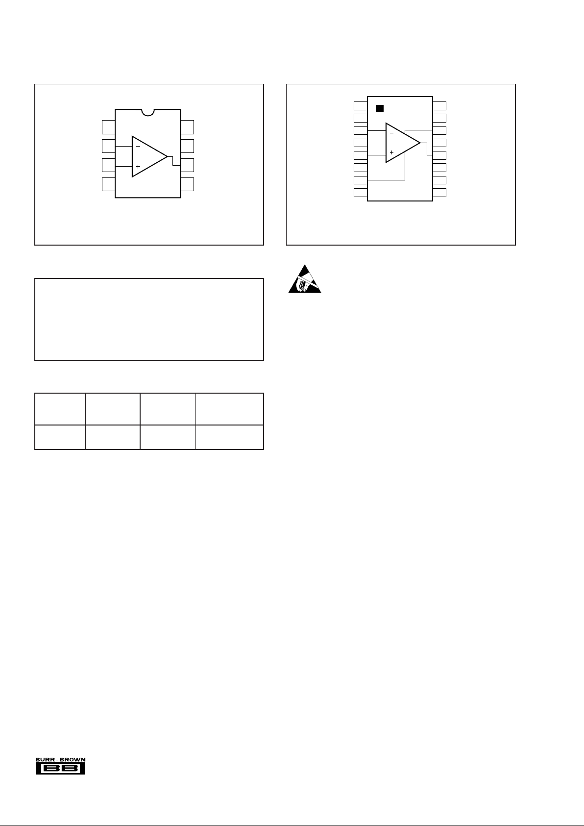
Top View
DIP
PIN CONFIGURATION
Top View
SO-16
1
2
3
4
5
6
7
8
NC
NC
–In
NC
+In
NC
–V
S
NC
NC: No Internal Connection.
Solder to ground plane for
improved heat dissipation.
16
15
14
13
12
11
10
9
NC
NC
+V
S
NC
V
O
NC
NC
NC
PIN CONFIGURATION
1
2
3
4
8
7
6
5
NC
–In
+In
–V
NC
+V
V
NC
S
S
NC: No Internal Connection.
Solder to ground plane for
improved heat dissipation.
O
PACKAGE/ORDERING INFORMATION
PACKAGE SPECIFIED
DRAWING TEMPERATURE
PRODUCT PACKAGE NUMBER
(1)
RANGE
OPA603AP Plastic DIP 006 –25°C to +85°C
OPA603AU SO-16 211 –25°C to +85°C
NOTE: (1) For detailed drawing and dimension table, please see end of data
sheet, or Appendix C of Burr-Brown IC Data Book.
ABSOLUTE MAXIMUM RATINGS
Supply Voltage................................................................................... ±18V
Input Voltage Range ............................................................................ ±V
S
Differential Input Voltage ..................................................................... ±6V
Power Dissipation ........................................................See derating curve
Operating Temperature ................................................................. +100°C
Storage Temperature..................................................................... +150°C
Junction Temperature .................................................................... +150°C
Lead Temperature (soldering, 10s) ............................................... +300°C
(soldering SO-16 package, 3s) ...................... +260°C
ELECTROSTATIC
DISCHARGE SENSITIVITY
This integrated circuit can be damaged by ESD. Burr-Brown
recommends that all integrated circuits be handled with
appropriate precautions. Failure to observe proper handling and
installation procedures can cause damage.
ESD damage can range from subtle performance degradation to
complete device failure. Precision integrated circuits may be more
susceptible to damage because very small parametric changes
could cause the device not to meet its published specifications.
 Loading...