

Burr Brown OPA552PA, OPA551FA, OPA551UA-2K5, OPA551PA, OPA551FA-500 Datasheet
...
1
OPA551, OPA552
®
®
OPA551
OPA552
©1999 Burr-Brown Corporation PDS-1472A Printed in U.S.A. July, 1999
High-Voltage, High-Current
OPERA TIONAL AMPLIFIERS
DESCRIPTION
The OPA551 and OPA552 are low cost op amps with
high-voltage (60V) and high-current (200mA) capability.
The OPA551 is unity-gain stable and features high
slew rate (15Vµs) and wide bandwidth (3MHz). The
OPA552 is optimized for gains of 5 or greater, and
offers higher speed with a slew rate of 24V/µs and a
bandwidth of 12MHz. Both are suitable for telephony,
audio, servo, and test applications.
These laser-trimmed, monolithic integrated circuits
provide excellent low-level accuracy along with high
output swing. High performance is maintained as the
amplifier swings to its specified limits.
The OPA551 and OPA552 are internally protected
against over-temperature conditions and current overloads. The thermal shutdown indicator “flag” provides
a current output to alert the user when thermal shutdown has occurred.
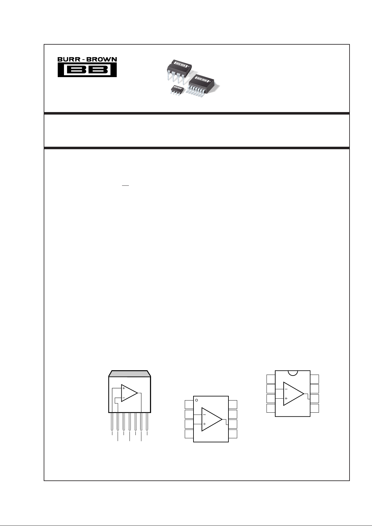
The OPA551 and OPA552 are available in DIP-8 and
SO-8 packages, as well as a DDPAK-7 surfacemount plastic power package. They are specified for
operation over the extended industrial temperature
range, –40°C to +125°C.
FEATURES
● WIDE SUPPLY RANGE: ±4V to ±30V
● HIGH OUTPUT CURRENT: 200mA Continuous
● LOW NOISE: 14nV/√Hz
● FULLY PROTECTED:
Thermal Shutdown
Output Current-Limited
● THERMAL SHUTDOWN INDICATOR
● WIDE OUTPUT SWING: 2V From Rail
● FAST SLEW RATE:
OPA551: 15V/µs
OPA552: 24V/µs
● WIDE BANDWIDTH:
OPA551: 3MHz
OPA552: 12MHz
● PACKAGES: DIP-8, SO-8, or DDPAK-7
APPLICATIONS
● TELEPHONY
● TEST EQUIPMENT
● AUDIO AMPLIFIER
● TRANSDUCER EXCITATION
● SERVO DRIVER
International Airport Industrial Park • Mailing Address: PO Box 11400, Tucson, AZ 85734 • Street Address: 6730 S. Tucson Blvd., Tucson, AZ 85706 • Tel: (520) 746-1111
Twx: 910-952-1111 • Internet: http://www.burr-brown.com/ • Cable: BBRCORP • Telex: 066-6491 • FAX: (520) 889-1510 • Immediate Product Info: (800) 548-6132
OPA551
OPA551
OPA551
For most current data sheet and other product
information, visit www.burr-brown.com
1
2
3
4
8
7
6
5
Flag
V+
Out
V–
V–
–In
+In
V–
OPA551, OPA552
SO-8 (U)
1
2
3
4
8
7
6
5
Flag
V+
Out
NC
NC
–In
+In
V–
OPA551, OPA552
DIP-8 (P)
NOTE: Tab is
connected to
V– supply.
NC
V–
V+
Out
+In
–In
1234
5
6
Flag
7
DDPAK-7 Surface-Mount (F)
OPA551, OPA552

2
OPA551, OPA552
®
SPECIFICATIONS: VS = ±30V
OPA551
At T
J
= +25°C
(1)
, RL = 3kΩ connected to ground and V
OUT
= 0V, unless otherwise noted.
Boldface limits apply over the specified junction temperature range, T
J
= –40°C to +125°C.
OPA551UA, PA, FA
PARAMETER CONDITION MIN TYP MAX UNITS
OFFSET VOLTAGE
Input Offset Voltage V
OS
VCM = 0V, IO = 0 ±1 ±3mV
T
J
= –40°C to +125°C ±5 mV
vs Temperature dVOS/dT ±7 µV/°C
vs Power Supply PSRR V
S
= ±4V to ±30V, VCM = 0V 10 30 µV/V
INPUT BIAS CURRENT
Input Bias Current I
B
±20 ±100 pA
Input Offset Current I
OS
±3 ±100 pA
NOISE
Input Voltage Noise Density, f = 1kHz e
n
14 nV/√Hz
Current Noise Density, f = 1kHz i
n
3.5 fA/√Hz
INPUT VOLTAGE RANGE
Common-Mode Voltage Range V
CM
(V–) + 2.5 (V+) – 2.5 V
Common-Mode Rejection Ratio CMRR –27.5V
< VCM < +27.5V 92 102 dB
INPUT IMPEDANCE
Differential 10
13
|| 2 Ω || pF
Common-Mode 10
13
|| 6 Ω || pF
OPEN-LOOP GAIN
Open-Loop Voltage Gain A
OL
RL = 3kΩ, –28V < VO < +28V 110 126 dB
T
J
= –40°C to +125°CR
L
= 3kΩ, –28V < VO < +28V 100 dB
R
L
= 300Ω, –27V < VO < +27V 120 dB
FREQUENCY RESPONSE
Gain-Bandwidth Product GBW 3 MHz
Slew Rate SR G = 1 ±15 V/µs
Settling Time: 0.1% G = 1, C
L
= 100pF, 10V Step 1.3 µs
0.01% G = 1, C
L
= 100pF, 10V Step 2 µs
Total Harmonic Distortion + Noise, f = 1kHz THD+N
VO = 15Vrms, RL = 3kΩ, G = 3 0.0005 %
VO = 15Vrms, RL = 300Ω, G = 3 0.0005 %
Overload Recovery Time V
IN
• Gain = V
S
1 µs
OUTPUT
Voltage Output V
OUT
IO = 200mA (V–) + 3.0 (V+) – 3.0 V
T
J
= –40°C to +125°CI
O
= 200mA (V–) + 3.5 (V+) – 3.5 V
I
O
= 10mA (V–) + 2.0 (V+) – 2.0 V
TJ = –40°C to +125°CI
O
= 10mA (V–) + 2.5 (V+) – 2.7 V
Maximum Continuous Current Output: dc I
O
Package Dependent—See Text ±200 mA
Short-Circuit Current I
SC
±380 mA
Capacitive Load Drive C
LOAD
Stable Operation See Typical Curve
SHUTDOWN FLAG
Thermal Shutdown Status Output
Normal Operation Sourcing 0.05 1 µA
Thermally Shutdown Sourcing 80 120 160 µA
Voltage Compliance Range V– (V+) – 1.5 V
Junction Temperature
Shutdown 160 °C
Reset from Shutdown 140 °C
POWER SUPPLY
Specified Voltage V
S
±30 V
Operating Voltage Range ±4 ±30 V
Quiescent Current I
Q
IO = 0 ±7 ±8.5 mA
T
J
= –40°C to +125°C ±10 mA
TEMPERATURE RANGE
Specified Range T
J
–40 +125 °C
Operating Range T
J
–55 +125 °C
Storage Range T
A
–65 +150 °C
Thermal Resistance
SO-8 Surface Mount
θ
JA
90 °C/W
DIP-8
θ
JA
100 °C/W
DDPak-7
θ
JA
65 °C/W
DDPak-7
θ
JC
3 °C/W
NOTES: (1) All tests are high-speed tested at +25°C ambient temperature. Effective junction temperature is +25°C unless otherwise noted.

3
OPA551, OPA552
®
SPECIFICATIONS: VS = ±30V
OPA552
At T
J
= +25°C
(1)
, RL = 3kΩ connected to Ground and V
OUT
= 0V, unless otherwise noted.
Boldface limits apply over the specified junciton temperature range, T
J
= –40°C to +125°C.
OPA552UA, PA, FA
PARAMETER CONDITION MIN TYP MAX UNITS
OFFSET VOLTAGE
Input Offset Voltage V
OS
VCM = 0V, IO = 0 ±1 ±3mV
TJ = –40°C to +125°C ±5 mV
vs Temperature dV
OS
/dT ±7 µV/°C
vs Power Supply PSRR V
S
= ±4V to ±30V, VCM = 0V 10 30 µV/V
INPUT BIAS CURRENT
Input Bias Current I
B
±20 ±100 pA
Input Offset Current I
OS
±3 ±100 pA
NOISE
Input Voltage Noise Density, f = 1kHz e
n
14 nV/√Hz
Current Noise Density, f = 1kHz i
n
3.5 fA/√Hz
INPUT VOLTAGE RANGE
Common-Mode Voltage Range V
CM
(V–) + 2.5 (V+) – 2.5 V
Common-Mode Rejection Ratio CMRR –27.5V
< VCM < +27.5V 92 102 dB
INPUT IMPEDANCE
Differential 1013 || 2 Ω || pF
Common-Mode 1013 || 6 Ω || pF
OPEN-LOOP GAIN
Open-Loop Voltage Gain A
OL
RL = 3kΩ, –28V < VO < +28V 110 126 dB
T
J
= –40°C to +125°CR
L
= 3kΩ, –28V < VO < +28V 100 dB
R
L
= 300Ω, –27V < VO < +27V 120 dB
FREQUENCY RESPONSE
Gain-Bandwidth Product GBW 12 MHz
Slew Rate SR G = 5 ±24 V/µs
Settling Time: 0.1% G = 5, C
L
= 100pF, 10V Step 2.2 µs
0.01% G = 5, C
L
= 100pF, 10V Step 3 µs
Total Harmonic Distortion + Noise, f = 1kHz THD+N
VO = 15Vrms, RL = 3kΩ, G = 5 0.0005 %
V
O
= 15Vrms, RL = 300Ω, G = 5 0.0005 %
Overload Recovery Time V
IN
• Gain = V
S
1 µs
OUTPUT
Voltage Output V
OUT
IO = 200mA (V–) + 3.0 (V+) – 3.0 V
T
J
= –40°C to +125°CI
O
= 200mA (V–) + 3.5 (V+) – 3.5 V
I
O
= 10mA (V–) + 2.0 (V+) – 2.0 V
T
J
= –40°C to +125°CI
O
= 10mA (V–) + 2.5 (V+) – 2.7 V
Maximum Continuous Current Output: dc IOPackage Dependent—See Text ±200 mA
Short-Circuit Current I
SC
±380 mA
Capacitive Load Drive C
LOAD
Stable Operation See Typical Curve
SHUTDOWN FLAG
Thermal Shutdown Status Output
Normal Operation Sourcing 0.05 1 µA
Thermally Shutdown Sourcing 80 120 160 µA
Voltage Compliance Range V– (V+) – 1.5 V
Junction Temperature
Shutdown 160 °C
Reset from Shutdown 140 °C
POWER SUPPLY
Specified Voltage V
S
±30 V
Operating Voltage Range ±4 ±30 V
Quiescent Current I
Q
IO = 0 ±7 ±8.5 mA
T
J
= –40°C to +125°C ±10 mA
TEMPERATURE RANGE
Specified Range T
J
–40 +125 °C
Operating Range T
J
–55 +125 °C
Storage Range T
A
–65 +150 °C
Thermal Resistance
SO-8 Surface Mount
θ
JA
90 °C/W
DIP-8
θ
JA
100 °C/W
DDPak-7
θ
JA
65 °C/W
DDPak-7
θ
JC
3 °C/W
NOTES: (1) All tests are high-speed tested at +25°C ambient temperature. Effective junction temperature is +25°C unless otherwise noted.

4
OPA551, OPA552
®
ABSOLUTE MAXIMUM RATINGS
(1)
Output Current ................................................................. See SOA Curve
Supply Voltage, V+ to V– ................................................................... 60V
Input Voltage Range ....................................... (V–) – 0.5V to (V+) + 0.5V
Operating Temperature ..................................................–55°C to +125°C
Storage Temperature .....................................................–65°C to +150°C
Junction Temperature .................................................................... +150°C
Lead Temperature (soldering 10s, DIP-8) ...................................... 300°C
(soldering 3s, SO-8 and DDPAK) .................... 240°C
ESD Capability (Human Body Model) ............................................. 3000V
NOTE: (1) Stresses above these ratings may cause permanent damage.
Exposure to absolute maximum conditions for extended periods may degrade
device reliability.
ELECTROSTATIC
DISCHARGE SENSITIVITY
This integrated circuit can be damaged by ESD. Burr-Brown
recommends that all integrated circuits be handled with
appropriate precautions. Failure to observe proper handling
and installation procedures can cause damage.
ESD damage can range from subtle performance degradation to complete device failure. Precision integrated circuits
may be more susceptible to damage because very small
parametric changes could cause the device not to meet its
published specifications.
The information provided herein is believed to be reliable; however, BURR-BROWN assumes no responsibility for inaccuracies or omissions. BURR-BROWN assumes no responsibility
for the use of this information, and all use of such information shall be entirely at the user’s own risk. Prices and specifications are subject to change without notice. No patent rights or
licenses to any of the circuits described herein are implied or granted to any third party. BURR-BROWN does not authorize or warrant any BURR-BROWN product for use in life support
devices and/or systems.
PACKAGE /ORDERING INFORMATION
PACKAGE SPECIFIED
DRAWING TEMPERATURE PACKAGE ORDERING TRANSPORT
PRODUCT PACKAGE NUMBER
(1)
RANGE MARKING NUMBER
(2)
MEDIA
OPA551UA SO-8 182 –40°C to +125°C OPA551UA OPA551UA Rails
"" " " "OPA551UA/2K5 Tape and Reel
OPA551PA DIP-8 006 –40°C to +125°C OPA551PA OPA551PA Rails
OPA551FA DDPAK-7 328 –40°C to +125°C OPA551FA OPA551FA Rails
"" " " "OPA551FA/500 Tape and Reel
OPA552UA SO-8 182 –40°C to +125°C OPA552UA OPA552UA Rails
"
""""OPA552UA/2K5 Tape and Reel
OPA552PA DIP-8 006 –40°C to +125°C OPA552PA OPA552PA Rails
OPA552FA DDPAK-7 328 –40°C to +125°C OPA552FA OPA552FA Rails
"" " " "OPA552FA/500 Tape and Reel
NOTES: (1) For detailed drawing and dimension table, please see end of data sheet, or Appendix C of Burr-Brown IC Data Book. (2) Products followed by a slash
(/) are only available in Tape and Reel in the quantities indicated (e.g., /2K5 indicates 2500 devices per reel). Ordering 2500 pieces of “OPA551UA/2K5” will get
a single 2500-piece Tape and Reel. For detailed Tape and Reel mechanical information, refer to Appendix B of Burr-Brown IC Data Book.
5
OPA551, OPA552
®
TYPICAL PERFORMANCE CURVES
At T
J
= +25°C, VS = ±30V and RL = 3kΩ, unless otherwise noted.
All temperatures are junction temperatures unless otherwise noted. Refer to the Applications Information section to calculate junction temperatures from ambient
temperatures for a specific configuration.
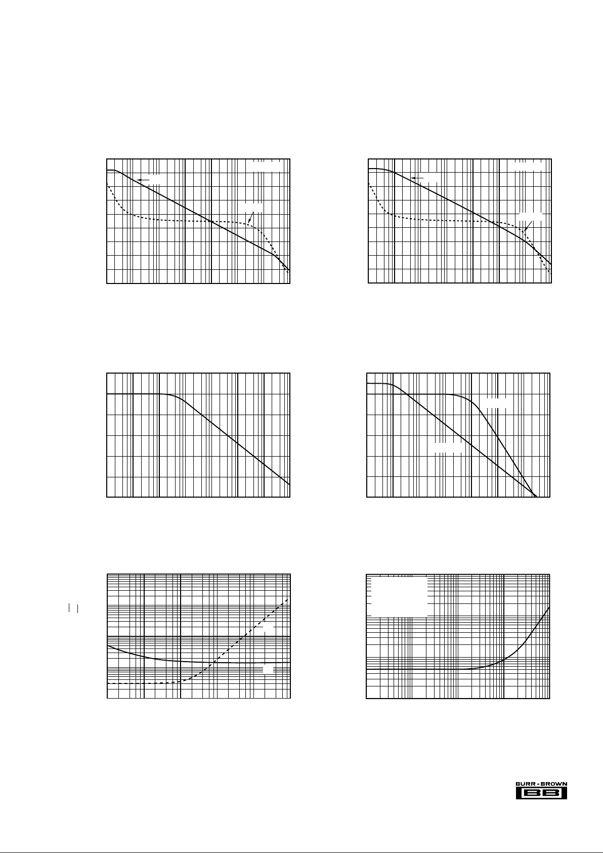
120
100
80
60
40
20
0
1 10 100 1k 10k 100k 1M 10M
Frequency (Hz)
CMRR (dB)
COMMON-MODE REJECTION RATIO vs FREQUENCY
120
100
80
60
40
20
0
1 10 100 1k 10k 100k 1M 10M
Frequency (Hz)
PSRR (dB)
POWER SUPPLY REJECTION RATIO vs FREQUENCY
–PSRR
+PSRR
140
120
100
80
60
40
20
0
–20
–40
0
–20
–40
–60
–80
–100
–120
–140
–160
–180
1 10 100 1k 10k 100k 1M 10M
Frequency (Hz)
Gain (dB)
OPEN-LOOP GAIN AND PHASE vs FREQUENCY
OPA552
Phase (°)
Phase
OPA552
Gain
10k
1k
100
10
1
INPUT VOLTAGE AND CURRENT NOISE
SPECTRAL DENSITY vs FREQUENCY
Voltage Noise (nV/√Hz)
Current Noise (fA/√Hz)
10 100 1k 10k 100k 1M
Frequency (Hz)
i
n
e
n
0.1
0.01
0.001
0.0001
TOTAL HARMONIC DISTORTION + NOISE
vs FREQUENCY
Frequency (Hz)
1 100 1k 10k 100k
THD+N (%)
VO = 15Vrms
R
L
= 3kΩ, 300Ω
G = 3 (OPA551)
G = 5 (OPA552)
140
120
100
80
60
40
20
0
–20
–40
0
–20
–40
–60
–80
–100
–120
–140
–160
–180
1 10 100 1k 10k 100k 1M 10M
Frequency (Hz)
Gain (dB)
OPEN-LOOP GAIN AND PHASE vs FREQUENCY
OPA551
Phase (°)
Phase
Gain
OPA551
 Loading...