

BURR-BROWN OPA551, OPA552 User Manual
OPA551
O
P
A
5
5
O
P
A
5
5
1
1
SBOS100A – JULY 1999 – REVISED OCTOBER 2003
High-Voltage, High-Current
OPERATIONAL AMPLIFIERS
OPA551
OPA552
FEATURES
● WIDE SUPPLY RANGE: ±4V to ±30V
● HIGH OUTPUT CURRENT: 200mA Continuous
● LOW NOISE: 14nV/√Hz
● FULLY PROTECTED:
Thermal Shutdown
Output Current-Limited
● THERMAL SHUTDOWN INDICATOR
● WIDE OUTPUT SWING: 2V From Rail
● FAST SLEW RATE:
OPA551: 15V/µs
OPA552: 24V/µs
● WIDE BANDWIDTH:
OPA551: 3MHz
OPA552: 12MHz
● PACKAGES: DIP-8, SO-8, or DDPAK-7
APPLICATIONS
● TELEPHONY
● TEST EQUIPMENT
● AUDIO AMPLIFIERS
● TRANSDUCER EXCITATION
● SERVO DRIVERS
DESCRIPTION
The OPA551 and OPA552 are low cost op amps with highvoltage (60V) and high-current (200mA) capability.
The OPA551 is unity-gain stable and features high slew rate
(15Vµs) and wide bandwidth (3MHz). The OPA552 is
optimized for gains of 5 or greater, and offers higher speed
with a slew rate of 24V/µs and a bandwidth of 12MHz. Both
are suitable for telephony, audio, servo, and test applications.
These laser-trimmed, monolithic integrated circuits provide
excellent low-level accuracy along with high output swing.
High performance is maintained as the amplifier swings to
its specified limits.
The OPA551 and OPA552 are internally protected against
over-temperature conditions and current overloads. The
thermal shutdown indicator “flag” provides a current output
to alert the user when thermal shutdown has occurred.
The OPA551 and OPA552 are available in DIP-8 and
SO-8 packages, as well as a DDPAK-7 surface-mount
plastic power package. They are specified for operation
over the extended industrial temperature range, –40°C to
+125°C.
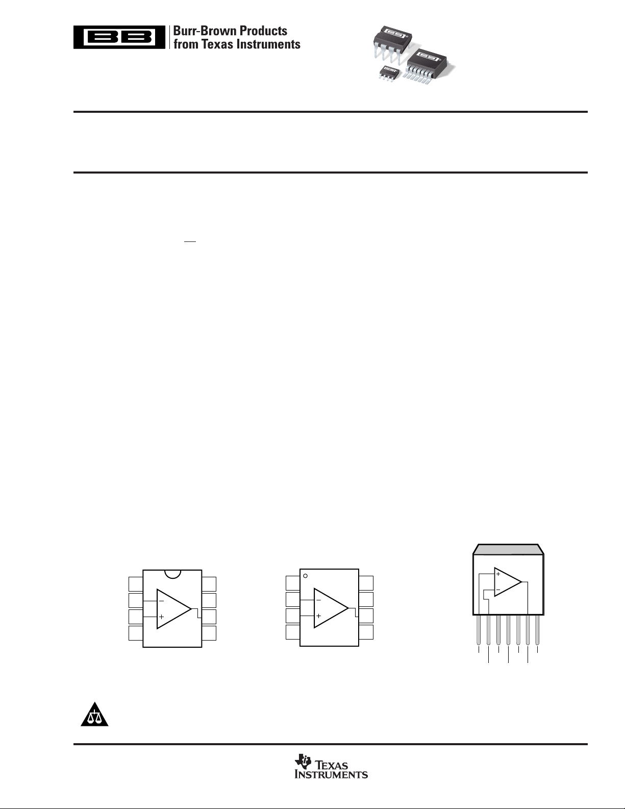
OPA551, OPA552
OPA551, OPA552
NC
1
–In
2
+In
3
V–
4
DIP-8 (P)
Please be aware that an important notice concerning availability, standard warranty, and use in critical applications of
Texas Instruments semiconductor products and disclaimers thereto appears at the end of this data sheet.
All trademarks are the property of their respective owners.
PRODUCTION DATA information is current as of publication date.
Products conform to specifications per the terms of Texas Instruments
standard warranty. Production processing does not necessarily include
testing of all parameters.
Flag
8
V+
7
Out
6
NC
5
V–
–In
+In
V–
OPA551, OPA552
1
2
3
4
SO-8 (U)
www.ti.com
Flag
8
V+
7
Out
6
V–
5
NOTE: Tab is
connected to
V– supply.
Copyright © 1999-2003, Texas Instruments Incorporated
1234
+In
–In
DDPAK-7 Surface-Mount (F)
NC
V–
6
7
5
V+
Flag
Out

SPECIFICATIONS: VS = ±30V
OPA551
At T
J
Boldface limits apply over the specified junction temperature range, T
PARAMETER CONDITION MIN TYP MAX UNITS
OFFSET VOLTAGE
Input Offset Voltage V
T
vs Temperature dVOS/dT ±7 µV/°C
vs Power Supply PSRR V
INPUT BIAS CURRENT
Input Bias Current I
Input Offset Current I
NOISE
Input Voltage Noise Density, f = 1kHz e
Current Noise Density, f = 1kHz i
INPUT VOLTAGE RANGE
Common-Mode Voltage Range V
Common-Mode Rejection Ratio CMRR –27.5V
INPUT IMPEDANCE
Differential 10
Common-Mode 10
OPEN-LOOP GAIN
Open-Loop Voltage Gain A
T
FREQUENCY RESPONSE
Gain-Bandwidth Product GBW 3 MHz
Slew Rate SR G = 1 ±15 V/µs
Settling Time: 0.1% G = 1, C
Total Harmonic Distortion + Noise, f = 1kHz THD+N
Overload Recovery Time V
OUTPUT
Voltage Output V
T
TJ = –40°C to +125°CI
Maximum Continuous Current Output: dc I
Short-Circuit Current I
Capacitive Load Drive C
SHUTDOWN FLAG
Thermal Shutdown Status Output
Normal Operation Sourcing 0.05 1 µA
Thermally Shutdown Sourcing 80 120 160 µA
Voltage Compliance Range V– (V+) – 1.5 V
Junction Temperature
Shutdown 160 °C
Reset from Shutdown 140 °C
POWER SUPPLY
Specified Voltage V
Operating Voltage Range ±4 ±30 V
Quiescent Current I
T
TEMPERATURE RANGE
Specified Range T
Operating Range T
Storage Range T
Thermal Resistance
SO-8 Surface Mount
DIP-8
DDPak-7
DDPak-7
NOTES: (1) All tests are high-speed tested at +25°C ambient temperature. Effective junction temperature is +25°C unless otherwise noted.
(1)
= +25°C
, RL = 3kΩ connected to ground and V
= 0V, unless otherwise noted.
OUT
= –40°C to +125°C.
J
OPA551UA, PA, FA
= –40°C to +125°C ±5 mV
J
= –40°C to +125°CR
J
OS
B
OS
n
n
CM
OL
0.01% G = 1, C
VCM = 0V, IO = 0 ±1 ±3mV
= ±4V to ±30V, VCM = 0V 10 30 µV/V
S
±20 ±100 pA
±3 ±100 pA
14 nV/√Hz
3.5 fA/√Hz
(V–) + 2.5 (V+) – 2.5 V
< VCM < +27.5V 92 102 dB
13
|| 2 Ω || pF
13
|| 6 Ω || pF
RL = 3kΩ, –28V < VO < +28V 110 126 dB
= 3kΩ, –28V < VO < +28V 100 dB
L
R
= 300Ω, –27V < VO < +27V 120 dB
L
= 100pF, 10V Step 1.3 µs
L
= 100pF, 10V Step 2 µs
VO = 15Vr ms, RL = 3kΩ, G = 3 0.0005 %
L
VO = 15Vrms, RL = 300Ω, G = 3 0.0005 %
• Gain = V
IN
= –40°C to +125°CI
J
= –40°C to +125°C ±10 mA
J
OUT
Package Dependent—See Text ±200 mA
O
SC
LOAD
S
Q
J
J
A
θ
JA
θ
JA
θ
JA
θ
JC
IO = 200mA (V–) + 3.0 (V+) – 3.0 V
= 200mA (V–) + 3.5 (V+) – 3.5 V
O
I
= 10mA (V–) + 2.0 (V+) – 2.0 V
O
= 10mA (V–) + 2.5 (V+) – 2.7 V
O
Stable Operation See Typical Curve
IO = 0 ±7 ±8.5 mA
S
–40 +125 °C
–55 +125 °C
–65 +150 °C
1 µs
±380 mA
±30 V
90 °C/W
100 °C/W
65 °C/W
3 °C/W
2
www.ti.com
OPA551, OPA552
SBOS100A

SPECIFICATIONS: VS = ±30V
OPA552
At T
J
Boldface limits apply over the specified junciton temperature range, T
PARAMETER CONDITION MIN TYP MAX UNITS
OFFSET VOLTAGE
Input Offset Voltage V
T
vs Temperature dV
vs Power Supply PSRR V
INPUT BIAS CURRENT
Input Bias Current I
Input Offset Current I
NOISE
Input Voltage Noise Density, f = 1kHz e
Current Noise Density, f = 1kHz i
INPUT VOLTAGE RANGE
Common-Mode Voltage Range V
Common-Mode Rejection Ratio CMRR –27.5V
INPUT IMPEDANCE
Differential 1013 || 2 Ω || pF
Common-Mode 10
OPEN-LOOP GAIN
Open-Loop Voltage Gain A
T
FREQUENCY RESPONSE
Gain-Bandwidth Product GBW 12 MHz
Slew Rate SR G = 5 ±24 V/µs
Settling Time: 0.1% G = 5, C
Total Harmonic Distortion + Noise, f = 1kHz THD+N
Overload Recovery Time V
OUTPUT
Voltage Output V
T
T
Maximum Continuous Current Output: dc I
Short-Circuit Current I
Capacitive Load Drive C
SHUTDOWN FLAG
Thermal Shutdown Status Output
Normal Operation Sourcing 0.05 1 µA
Thermally Shutdown Sourcing 80 120 160 µA
Voltage Compliance Range V– (V+) – 1.5 V
Junction Temperature
Shutdown 160 °C
Reset from Shutdown 140 °C
POWER SUPPLY
Specified Voltage V
Operating Voltage Range ±4 ±30 V
Quiescent Current I
T
TEMPERATURE RANGE
Specified Range T
Operating Range T
Storage Range T
Thermal Resistance
SO-8 Surface Mount
DIP-8
DDPak-7
DDPak-7
NOTES: (1) All tests are high-speed tested at +25°C ambient temperature. Effective junction temperature is +25°C unless otherwise noted.
(1)
= +25°C
, RL = 3kΩ connected to Ground and V
= 0V, unless otherwise noted.
OUT
= –40°C to +125°C.
J
OPA552UA, PA, FA
= –40°C to +125°C ±5 mV
J
= –40°C to +125°CR
J
OS
/dT ±7 µV/°C
OS
B
OS
n
n
CM
OL
0.01% G = 5, C
= –40°C to +125°CI
J
= –40°C to +125°CI
J
= –40°C to +125°C ±10 mA
J
OUT
LOAD
θ
θ
θ
θ
O
SC
S
Q
J
J
A
JA
JA
JA
JC
VCM = 0V, IO = 0 ±1 ±3mV
= ±4V to ±30V, VCM = 0V 10 30 µV/V
S
±20 ±100 pA
±3 ±100 pA
14 nV/√Hz
3.5 fA/√Hz
(V–) + 2.5 (V+) – 2.5 V
< VCM < +27.5V 92 102 dB
13
|| 6 Ω || pF
RL = 3kΩ, –28V < VO < +28V 110 126 dB
= 3kΩ, –28V < VO < +28V 100 dB
L
RL = 300Ω, –27V < VO < +27V 120 dB
= 100pF, 10V Step 2.2 µs
L
= 100pF, 10V Step 3 µs
VO = 15Vr ms, RL = 3kΩ, G = 5 0.0005 %
V
L
= 15Vrms, RL = 300Ω, G = 5 0.0005 %
O
• Gain = V
IN
S
1 µs
IO = 200mA (V–) + 3.0 (V+) – 3.0 V
= 200mA (V–) + 3.5 (V+) – 3.5 V
O
IO = 10mA (V–) + 2.0 (V+) – 2.0 V
= 10mA (V–) + 2.5 (V+) – 2.7 V
Package Dependent—See Text ±200 mA
O
±380 mA
Stable Operation See Typical Curve
±30 V
IO = 0 ±7 ±8.5 mA
–40 +125 °C
–55 +125 °C
–65 +150 °C
90 °C/W
100 °C/W
65 °C/W
3 °C/W
OPA551, OPA552
SBOS100A
www.ti.com
3

ABSOLUTE MAXIMUM RATINGS
Output Current ................................................................. See SOA Curve
Supply Voltage, V+ to V– ................................................................... 60V
Input Voltage Range ....................................... (V–) – 0.5V to (V+) + 0.5V
Operating Temperature ..................................................–55°C to +125°C
Storage Temperature ..................................................... –65°C to +150°C
Junction Temperature .................................................................... +150°C
Lead Temperature (soldering 10s, DIP-8) ...................................... 300°C
(soldering 3s, SO-8 and DDPAK) .................... 240°C
ESD Capability (Human Body Model) ............................................. 3000V
NOTE: (1) Stresses above these ratings may cause permanent damage.
Exposure to absolute maximum conditions for extended periods may degrade
device reliability.
(1)
ELECTROSTATIC
DISCHARGE SENSITIVITY
This integrated circuit can be damaged by ESD. Burr-Brown
recommends that all integrated circuits be handled with
appropriate precautions. Failure to observe proper handling
and installation procedures can cause damage.
ESD damage can range from subtle performance degradation to complete device failure. Precision integrated circuits
may be more susceptible to damage because very small
parametric changes could cause the device not to meet its
published specifications.
PACKAGE/ORDERING INFORMATION
For the most current package and ordering information, see the Package Ordering Addendum at the end of this data sheet.
4
www.ti.com
OPA551, OPA552
SBOS100A
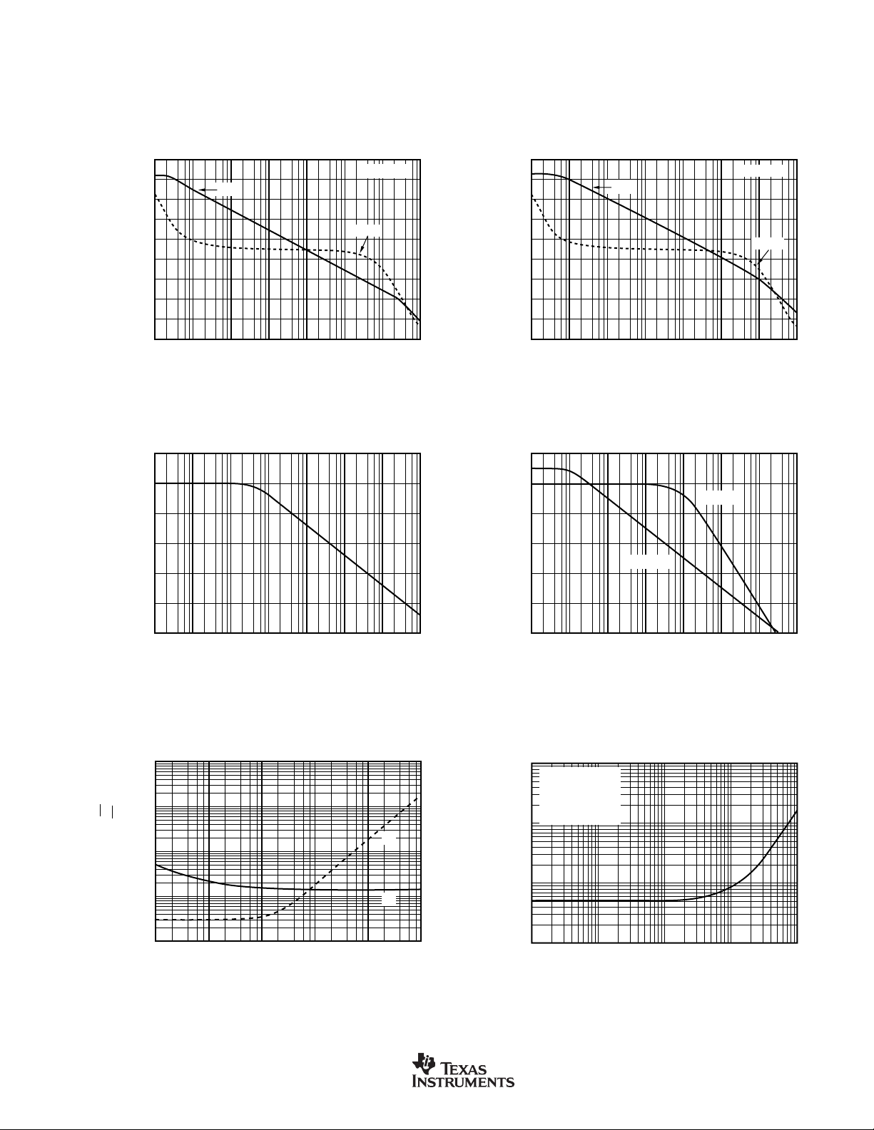
TYPICAL PERFORMANCE CURVES
120
100
80
60
40
20
0
1 10 100 1k 10k 100k 1M 10M
Frequency (Hz)
PSRR (dB)
POWER SUPPLY REJECTION RATIO vs FREQUENCY
–PSRR
+PSRR
0.1
0.01
0.001
0.0001
TOTAL HARMONIC DISTORTION + NOISE
vs FREQUENCY
Frequency (Hz)
1 100 1k 10k 100k
THD+N (%)
VO = 15Vrms
R
L
= 3kΩ, 300Ω
G = 3 (OPA551)
G = 5 (OPA552)
At T
= +25°C, VS = ±30V and RL = 3kΩ, unless otherwise noted.
J
All temperatures are junction temperatures unless otherwise noted. Refer to the Applications Information section to calculate junction temperatures from ambient
temperatures for a specific configuration.
OPEN-LOOP GAIN AND PHASE vs FREQUENCY
140
120
100
80
60
40
Gain (dB)
20
0
–20
–40
1 10 100 1k 10k 100k 1M 10M
COMMON-MODE REJECTION RATIO vs FREQUENCY
120
100
80
60
CMRR (dB)
40
Gain
OPA551
Phase
Frequency (Hz)
OPA551
0
–20
–40
–60
–80
–100
–120
–140
–160
–180
OPEN-LOOP GAIN AND PHASE vs FREQUENCY
140
120
100
80
60
40
Gain (dB)
Phase (°)
20
0
–20
–40
1 10 100 1k 10k 100k 1M 10M
OPA552
Gain
Frequency (Hz)
OPA552
Phase
0
–20
–40
–60
–80
–100
–120
–140
–160
–180
Phase (°)
20
0
1 10 100 1k 10k 100k 1M 10M
INPUT VOLTAGE AND CURRENT NOISE
10k
1k
100
10
Current Noise (fA/√Hz)
Voltage Noise (nV/√Hz)
1
10 100 1k 10k 100k 1M
SPECTRAL DENSITY vs FREQUENCY
Frequency (Hz)
Frequency (Hz)
i
n
e
n
OPA551, OPA552
SBOS100A
www.ti.com
5
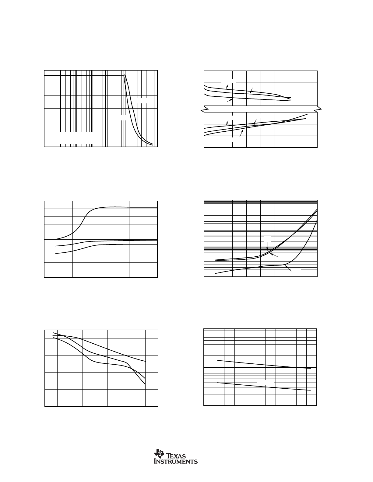
TYPICAL PERFORMANCE CURVES (Cont.)
At T
= +25°C, VS = ±30V and RL = 3kΩ, unless otherwise noted.
J
All temperatures are junction temperatures unless otherwise noted. Refer to the Applications Information section to calculate junction temperatures from ambient
temperatures for a specific configuration.
MAXIMUM OUTPUT VOLTAGE SWING
vs FREQUENCY
±30
±25
±20
OPA552
±15
±10
Maximum Output Voltage (V)
±5
Without Slew-Induced
OPA551
Distortion
0
1 10 100 1k 10k 100k 1M 10M
Frequency (Hz)
OPEN-LOOP GAIN, POWER SUPPLY REJECTION RATIO,
AND COMMON-MODE REJECTION RATIO
vs TEMPERATURE
130
125
120
A
OL
115
110
105
Gain (dB)
100
PSRR
CMRR
95
90
85
80
–75 –25 25 75 125
Ambient Temperature (°C)
(V+)
(V+)–1
OUTPUT VOLTAGE SWING vs OUTPUT CURRENT
+85°C
(V+)–2
(V+)–3
(V–)+3
–55°C
–55°C
(V–)+2
Output Voltage Swing (V)
(V–)+1
(V–)
0 50 100 150 200 250 300 350 400
INPUT BIAS CURRENT AND INPUT OFFSET CURRENT
100k
10k
1k
100
Current (pA)
10
1
–75 0–25–50 25 50 75 100 125
+25°C
+25°C
+85°C
Output Current (mA)
vs TEMPERATURE
+I
B
Ambient Temperature (°C)
–I
B
–I
OS
QUIESCENT CURRENT AND SHORT-CIRCUIT CURRENT
vs TEMPERATURE
9
8
7
6
5
(mA)
Q
4
I
3
2
1
0
I
Q
–I
SC
+I
SC
450
430
410
390
370
350
330
310
290
270
(mA)
SC
I
Gain Bandwidth Product (MHz)
–75 –50 –25 0 25 50 75 100 125 150
Temperature (°C)
6
www.ti.com
GAIN BANDWIDTH PRODUCT vs TEMPERATURE
100
OPA552
10
OPA551
1
–80 –60 –40 –20 0 20 40 60 80 100 120 140
Temperature (°C)
OPA551, OPA552
SBOS100A
 Loading...