

Burr Brown OPA549T Datasheet
®
For most current data sheet and other product
information, visit www.burr-brown.com
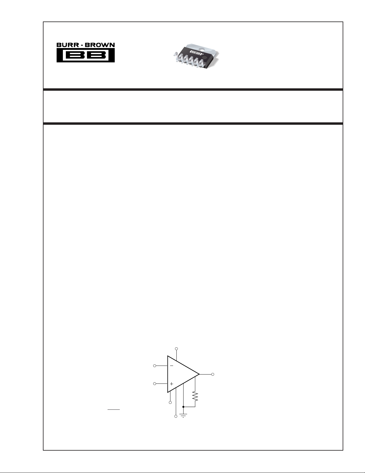
High-Voltage, High-Current
OPERATIONAL AMPLIFIER
OPA549
OPA549
FEATURES
● HIGH OUTPUT CURRENT:
8A Continuous
10A Peak
● WIDE POWER SUPPLY RANGE:
Single Supply: +8V to +60V
Dual Supply: ±4V to ±30V
● WIDE OUTPUT VOLTAGE SWING
● FULLY PROTECTED:
Thermal Shutdown
Adjustable Current Limit
● OUTPUT DISABLE CONTROL
● THERMAL SHUTDOWN INDICATOR
● HIGH SLEW RATE: 9V/µs
● CONTROL REFERENCE PIN
● 11-LEAD POWER ZIP PACKAGE
APPLICATIONS
● VALVE, ACTUATOR DRIVER
● SYNCHRO, SERVO DRIVER
● POWER SUPPLIES
● TEST EQUIPMENT
● TRANSDUCER EXCITATION
● AUDIO POWER AMPLIFIER
DESCRIPTION
The OPA549 is a low-cost, high-voltage/high-current
operational amplifier ideal for driving a wide variety
of loads. This laser-trimmed monolithic integrated
circuit provides excellent low-level signal accuracy,
and high output voltage and current.
The OPA549 operates from either single or dual supplies for design flexibility. The input common-mode
range extends below the negative supply.
The OPA549 is internally protected against overtemperature conditions and current overloads. In addition, the OPA549 provides an accurate, user-selected
current limit. Unlike other designs which use a “power”
resistor in series with the output current path, the
OPA549 senses the load indirectly. This allows the
current limit to be adjusted from 0A to 10A with a
resistor/potentiometer, or controlled digitally with a
voltage-out or current-out DAC.
The Enable/Status (E/S) pin provides two functions. It
can be monitored to determine if the device is in
thermal shutdown, and it can be forced low to disable
the output stage and effectively disconnect the load.
The OPA549 is available in an 11-lead power ZIP
package. Its copper tab allows easy mounting to a heat
sink for excellent thermal performance. Operation is
specified over the extended industrial temperature
range, –40°C to +85°C.
V+
OPA549
ES Pin
Forced Low: Output disabled
Indicates Low: Thermal shutdown
International Airport Industrial Park • Mailing Address: PO Box 11400, Tucson, AZ 85734 • Street Address: 6730 S. Tucson Blvd., Tucson, AZ 85706 • Tel: (520) 746-1111
Twx: 910-952-1111 • Internet: http://www.burr-brown.com/ • Cable: BBRCORP • Telex: 066-6491 • FAX: (520) 889-1510 • Immediate Product Info: (800) 548-6132
©
1999 Burr-Brown Corporation PDS-1450A Printed in U.S.A. November, 1999
E/S
V–
I
Ref
1 OPA549
V
LIM
R
O
R
sets the current limit
CL
value from 0A to 10A.
(Very Low Power Dissipation)
CL
®
SPECIFICATIONS: VS = ±2.25V to ±18V
Boldface limits apply over the specified temperature range, TA = –40°C to +85°C
At T
= +25°C, VS = ±30V, Ref = 0V, and E/S pin open, unless otherwise noted.
CASE
OPA549T
PARAMETER CONDITION MIN TYP MAX UNITS
OFFSET VOLTAGE V
Input Offset Voltage VCM = 0V, IO = 0 ±1 ±5mV
vs Temperature dV
vs Power Supply PSRR VS = ±4V to ±30V, Ref = V – 25 100 µV/V
INPUT BIAS CURRENT
Input Bias Current
(1)
(2)
vs Temperature T
Input Offset Current I
NOISE
Input Voltage Noise Density e
Current Noise Density i
INPUT VOLTAGE RANGE
Common-Mode Voltage Range: Positive V
Negative V
Common-Mode Rejection Ratio CMRR V
INPUT IMPEDANCE
Differential 10
Common-Mode 109 || 4 Ω || pF
OPEN-LOOP GAIN
Open-Loop Voltage Gain A
FREQUENCY RESPONSE
Gain Bandwidth Product GBW 0.9 MHz
Slew Rate SR G = 1, 50Vp-p Step, R
Full Power Bandwidth See Typical Curve
Settling Time: ±0.1% G = –10, 50V Step 20 µs
Total Harmonic Distortion + Noise
(3)
OUTPUT
Voltage Output, Positive I
Negative IO = –2A (V–) + 1.7 (V–) + 1.4 V
Positive I
Negative IO = –8A (V–) + 4.6 (V–) + 3.9 V
Negative R
Maximum Continuous Current Output: dc
Output Current Limit
Current Limit Range 0 to ±10 A
Current Limit Equation I
Current Limit Tolerance
(1)
Capacitive Load Drive (Stable Operation) C
Output Disabled
Leakage Current Output Disabled See Typical Curve
Output Capacitance Output Disabled 750 pF
OUTPUT ENABLE /STATUS (E/S) PIN
Shutdown Input Mode
High (output enabled) E/S Pin Open or Forced High (Ref) + 2.4 V
V
E/S
Low (output disabled) E/S Pin Forced Low (Ref) + 0.8 V
V
E/S
I
High (output enabled) E/S Pin Indicates High –50 µA
E/S
Low (output disabled) E/S Pin Indicates Low –55 µA
I
E/S
Output Disable Time 1 µs
Output Enable Time 3 µs
Thermal Shutdown Status Output
Normal Operation Sourcing 20µA (Ref) + 2.4 (Ref) + 3.5 V
Thermally Shutdown Sinking 5µA, T
Junction Temperature, Shutdown +160 °C
Reset from Shutdown +140 °C
Ref (Reference Pin for Control Signals)
Voltage Range V– (V+) – 8 V
(2)
Current
POWER SUPPLY
Specified Voltage V
Operating Voltage Range, (V+) – (V–) 8 60 V
Quiescent Current I
Quiescent Current in Shutdown Mode I
TEMPERATURE RANGE
Specified Range –40 +85 °C
Operating Range –40 +125 °C
Storage Range –55 +125 °C
Thermal Resistance,
Thermal Resistance,
NOTES: (1) High-speed test at T
Frequency” in the Typical Performance Curves section for additional power levels. (4) See “Safe Operating Area” (SOA) in the Typical Performance Curves section.
θ
JC
θ
JA
= +25°C. (2) Positive conventional current is defined as flowing into the terminal. (3) See “Total Harmonic Distortion + Noise vs
J
®
THD+N
(4)
(4)
ac
OS
OS
/dT T
I
B
OS
n
n
CM
CM
OL
= –40°C to +85°C ±20 µV/°C
CASE
V
= 0V –100 –500 nA
CM
= –40°C to +85°C ±0.5 nA/°C
CASE
V
= 0V ±5 ±50 nA
CM
f = 1kHz 70 nV/√Hz
f = 1kHz 1 pA/√Hz
Linear Operation (V+) – 3 (V+) – 2.3 V
Linear Operation (V–) – 0.1 (V–) – 0.2 V
= (V–) – 0.1V to (V+) – 3V 80 95 dB
CM
VO = ±25V, RL = 1kΩ 100 110 dB
VO = ±25V, RL = 4Ω 100 dB
f = 1kHz,RL = 4Ω,G = +3, Power = 25W
= 2A (V+) – 3.2 (V+) – 2.7 V
O
= 8A (V+) – 4.8 (V+) – 4.3 V
O
= 8Ω to V– (V–) + 0.3 (V–) + 0.1 V
L
Waveform Cannot Exceed 10A peak
R
LOAD
= 7.5kΩ (I
CL
S
I
Q
Connected to Ref IO = 0 ±26 ±35 mA
LIM
LIM
= ±5A), RL = 4Ω±200 ±500 mA
LIM
Connected to Ref ±6mA
No Heat Sink 30 °C/W
7
|| 6 Ω || pF
= 4Ω 9V/µs
L
0.015 %
±8A
8 Arms
= 15800 • 4.75V/(7500Ω + RCL)A
LIM
See Typical Curve
> 160°C (Ref) + 0.2 (Ref) + 0.8 V
J
–3.5 mA
±30 V
1.4 °C/W
2OPA549
ABSOLUTE MAXIMUM RATINGS
(1)
PACKAGE/ ORDERING INFORMATION
Output Current ................................................ See SOA Curve (Figure 6)
Supply Voltage, V+ to V– ................................................................... 60V
Input Voltage Range ....................................... (V–) – 0.5V to (V+) + 0.5V
Input Shutdown Voltage ................................................... Ref – 0.5 to V+
Operating Temperature ..................................................–40 °C to +125°C
Storage Temperature ..................................................... –55°C to +125°C
Junction Temperature ...................................................................... 150°C
Lead Temperature (soldering, 10s) ................................................. 300°C
ESD Capability (Human Body Model) ............................................. 2000V
NOTE: (1) Stresses above these ratings may cause permanent damage.
Exposure to absolute maximum conditions for extended periods may degrade device reliability.
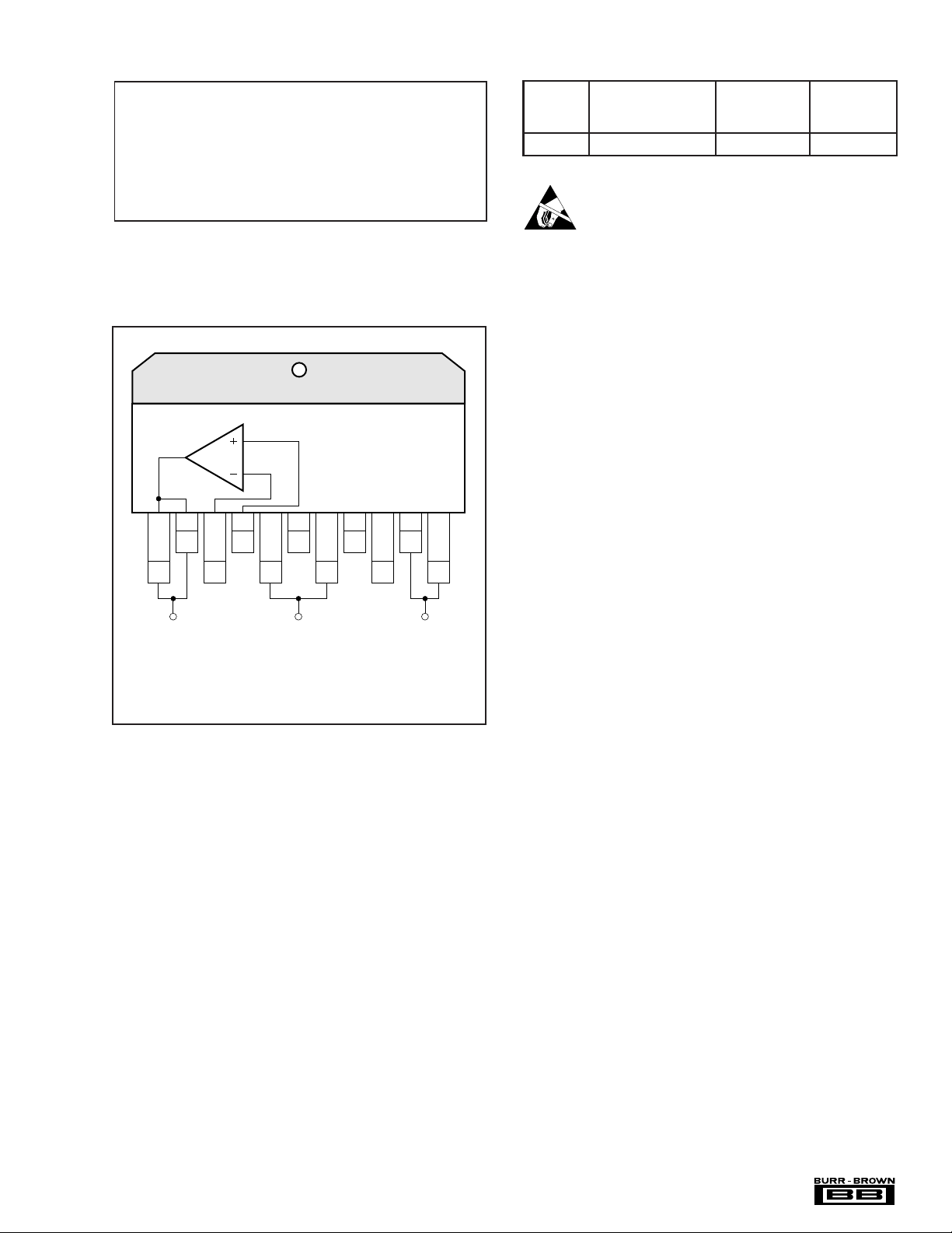
CONNECTION DIAGRAM
Tab connected to V–. Do not use to conduct current.
246810
1357911
+In
–In
Ref I
LIM
E/S
PACKAGE
DRAWING TEMPERATURE
PRODUCT PACKAGE NUMBER RANGE
OPA549T 11-Lead Power ZIP 242 –40°C to +85°C
ELECTROSTATIC
DISCHARGE SENSITIVITY
This integrated circuit can be damaged by ESD. Burr-Brown
recommends that all integrated circuits be handled with
appropriate precautions. Failure to observe proper handling
and installation procedures can cause damage.
ESD damage can range from subtle performance degradation to complete device failure. Precision integrated circuits
may be more susceptible to damage because very small
parametric changes could cause the device not to meet its
published specifications.
O
Connect both pins 1 and 2 to output.
Connect both pins 5 and 7 to V–.
Connect both pins 10 and 11 to V+.
V–
V+V
The information provided herein is believed to be reliable; however, BURR-BROWN assumes no responsibility for inaccuracies or omissions. BURR-BROWN assumes
no responsibility for the use of this information, and all use of such information shall be entirely at the user’s own risk. Prices and specifications are subject to change
without notice. No patent rights or licenses to any of the circuits described herein are implied or granted to any third party. BURR-BROWN does not authorize or warrant
any BURR-BROWN product for use in life support devices and/or systems.
3 OPA549
®
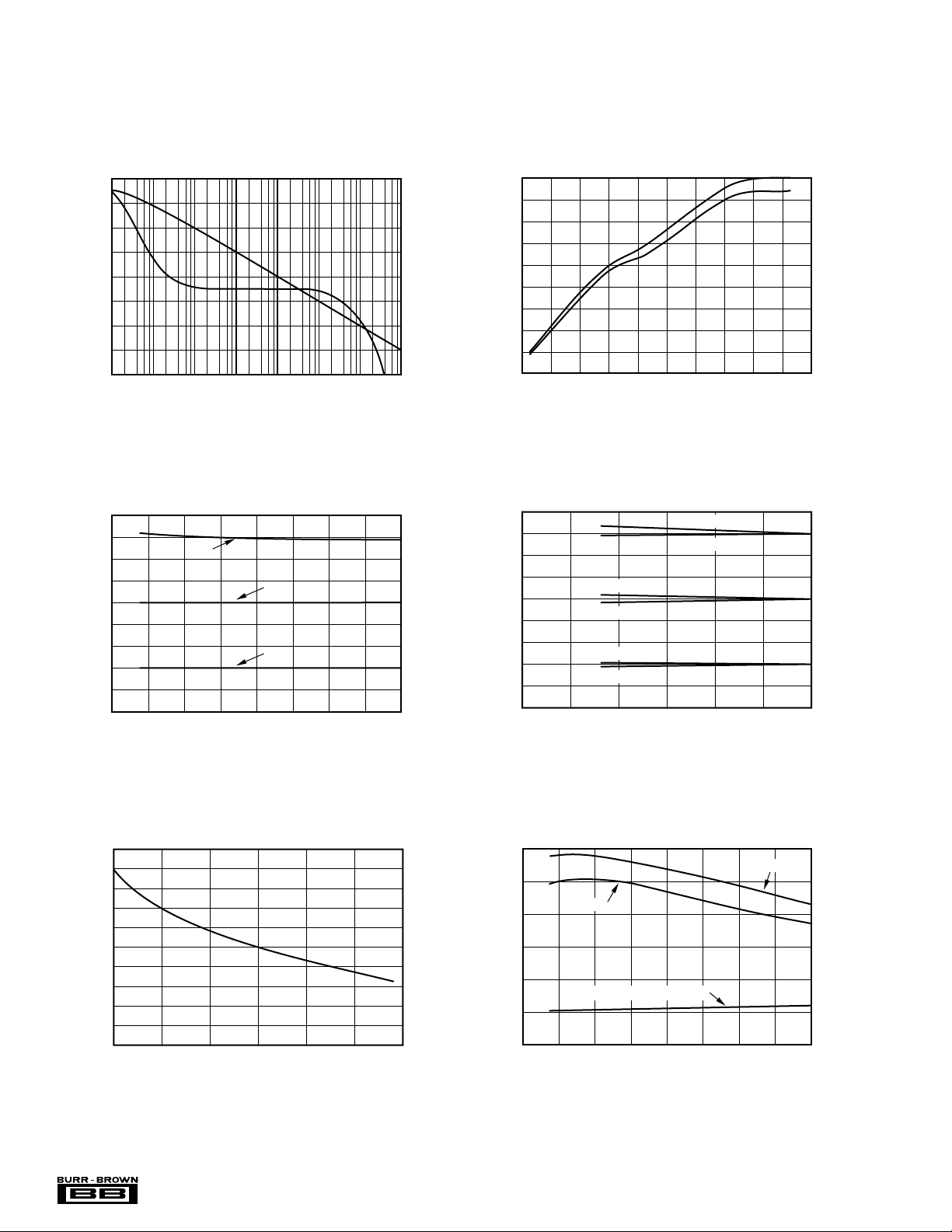
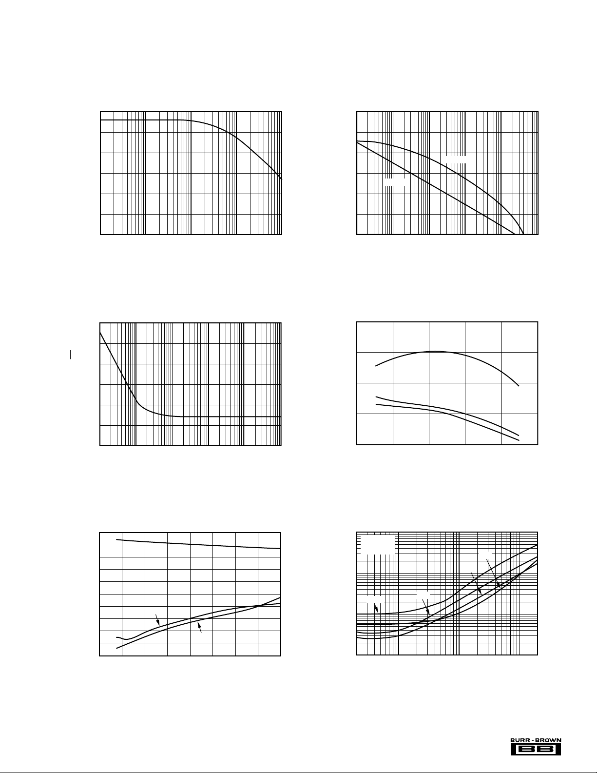
TYPICAL PERFORMANCE CURVES
At T
= +25°C, VS = ±30V and E/S pin open, unless otherwise noted.
CASE
OPEN-LOOP GAIN AND PHASE
vs FREQUENCY
120
100
80
60
40
Gain (dB)
20
0
–20
–40
1 10 100 1k 10k 100k 1M 10M
Frequency (Hz)
CURRENT LIMIT vs TEMPERATURE
9
8
7
6
8A
5A
5
4
3
Current Limit (A)
2A
2
1
0
–75 –50 –25 0 25 50 75 100 125
Temperature (°C)
0
–20
–40
–60
–80
–100
–120
–140
–160
–130
–120
–110
–100
–90
–80
Phase (°)
–70
Input Bias Current (nA)
–60
–50
–40
–60 –40 –20 0 20 40 60 80 140120100
9
8
7
6
5
4
3
Current Limit (A)
2
1
0
0 5 10 15 20 25 30
INPUT BIAS CURRENT vs TEMPERATURE
–I
B
+I
B
Temperature (°C)
CURRENT LIMIT vs SUPPLY VOLTAGE
+I
, 8A
LIM
–I
, 8A
LIM
+I
, 5A
LIM
–I
, 5A
LIM
+I
, 2A
LIM
–I
, 2A
LIM
Supply Voltage (V)
INPUT BIAS CURRENT
vs COMMON-MODE VOLTAGE
–200
–180
–160
–140
–120
–100
–80
–60
Input Bias Current (nA)
–40
–20
–0
–30 –20 –10 0 10 20 30
Common-Mode Voltage (V)
®
30
QUIESCENT CURRENT vs TEMPERATURE
VS = ±30V
25
20
VS = ±5V
15
10
Quiescent Current (mA)
5
IQ Shutdown (output disabled)
0
–75 –50 –25 0 25 50 75 100 125
Temperature (°C)
4OPA549
TYPICAL PERFORMANCE CURVES (Cont.)
10 100 1k 10k 100k 1M
120
100
80
60
40
20
0
Power Supply Rejection Ratio (dB)
Frequency (Hz)
POWER SUPPLY REJECTION RATIO
vs FREQUENCY
–PSRR
+PSRR
At T
= +25°C, VS = ±30V and E/S pin open, unless otherwise noted.
CASE
COMMON-MODE REJECTION RATIO vs FREQUENCY
100
90
80
70
60
50
Common-Mode Rejection (dB)
40
10 100 1k 10k 100k
Frequency (Hz)
OPEN-LOOP GAIN, COMMON-MODE REJECTION RATIO
300
VOLTAGE NOISE DENSITY vs FREQUENCY
120
AND POWER SUPPLY REJECTION RATIO
vs TEMPERATURE
250
200
150
100
Voltage Noise (nV/√Hz)
50
0
1 10 100 1k 10k 100k
Frequency (Hz)
GAIN-BANDWIDTH PRODUCT AND
1
0.9
0.8
0.7
0.6
0.5
0.4
0.3
0.2
Gain-Bandwidth Product (MHz)
0.1
0
–75 –50 –25 0 25 50 75 100 125
SLEW RATE vs TEMPERATURE
GBW
SR+
Temperature (°C)
SR–
16
15
14
13
12
11
10
Slew Rate (V/µs)
9
8
7
6
110
100
, CMRR, PSRR (dB)
OL
90
A
80
–75 –50 0 50 100
TOTAL HARMONIC DISTORTION + NOISE
1
G = +3
R
= 4Ω
L
0.1
0.1W
THD+N (%)
0.01
0.001
20 100 1k 10k 20k
A
OL
PSRR
CMRR
Temperature (°C)
vs FREQUENCY
1W
Frequency (Hz)
75W
10W
125
®
5 OPA549
 Loading...