

Burr Brown OPA544F, OPA544F-500, OPA544T-1, OPA544T Datasheet
®
High-Voltage, High-Current
OPERATIONAL AMPLIFIER
OPA544
FEATURES
● HIGH OUTPUT CURRENT: 2A min
● WIDE POWER SUPPLY RANGE:
±10 to ±35V
● SLEW RATE: 8V/µs
● INTERNAL CURRENT LIMIT
● THERMAL SHUTDOWN PROTECTION
● FET INPUT: I
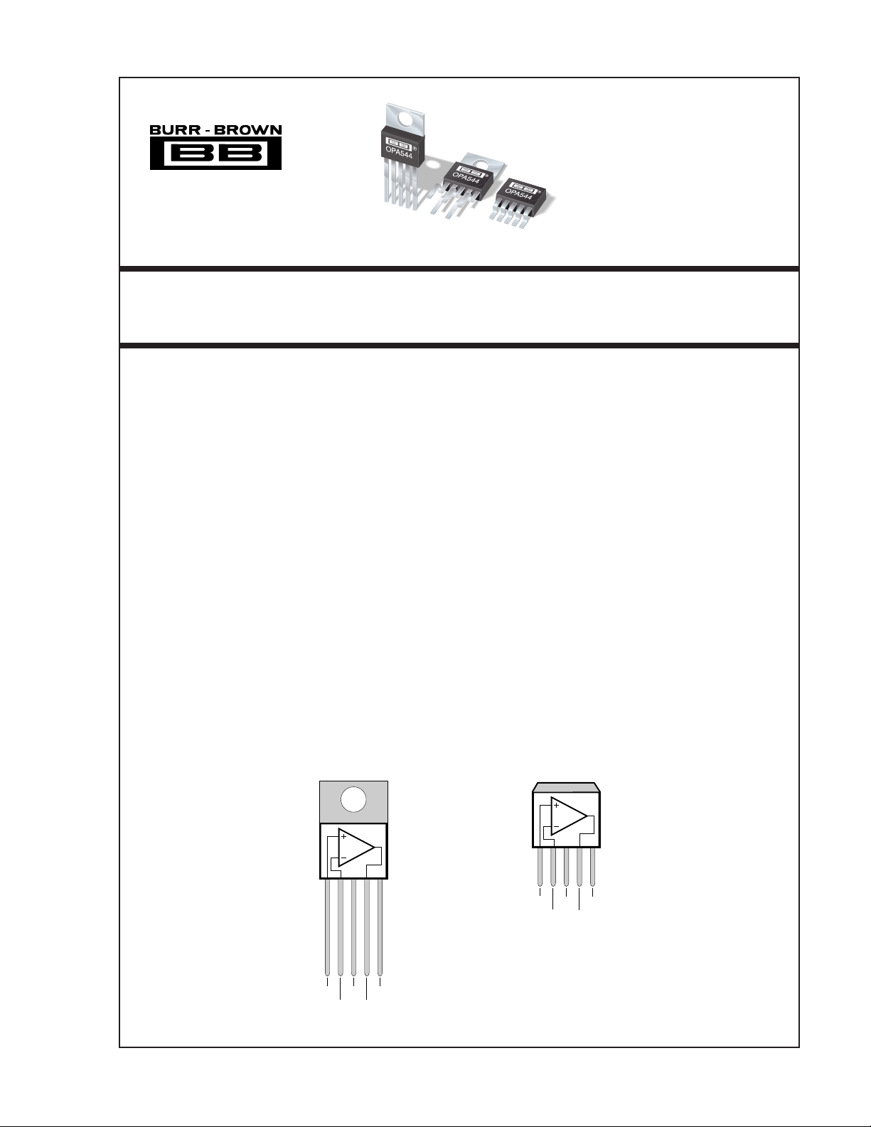
● 5-LEAD TO-220 PLASTIC PACKAGE
● 5-LEAD SURFACE MOUNT PACKAGE
= 100pA max
B
APPLICATIONS
● MOTOR DRIVER
● PROGRAMMABLE POWER SUPPLY
● SERVO AMPLIFIER
● VALVES, ACTUATOR DRIVER
● MAGNETIC DEFLECTION COIL DRIVER
● AUDIO AMPLIFIER
Tab is connected
to V– supply.
5-Lead TO-220
and
Stagger-Formed
TO-220
DESCRIPTION
The OPA544 is a high-voltage/high-current operational amplifier suitable for driving a wide variety of
high power loads. High performance FET op amp
circuitry and high power output stage are combined on
a single monolithic chip.
The OPA544 is protected by internal current limit and
thermal shutdown circuits.
The OPA544 is available in industry-standard
5-lead TO-220 and 5-lead surface-mount power packages. Its copper tab allows easy mounting to a heat
sink for excellent thermal performance. It is specified
for operation over the extended industrial temperature
range, –40°C to +85°C.
Tab is connected
to V– supply.
5-Lead
Surface Mount
1234
1234
+
V
IN
International Airport Industrial Park • Mailing Address: PO Box 11400, Tucson, AZ 85734 • Street Address: 6730 S. Tucson Blvd., Tucson, AZ 85706 • Tel: (520) 746-1111 • Twx: 910-952-1111
Internet: http://www.burr-brown.com/ • FAXLine: (800) 548-6133 (US/Canada Only) • Cable: BBRCORP • Telex: 066-6491 • FAX: (520) 889-1510 • Immediate Product Info: (800) 548-6132
5
V–
V+
–
V
V
IN
O
+
V
IN
5
V–
V+
–
V
V
IN
O
©1994 Burr-Brown Corporation PDS-1250B Printed in U.S.A. September, 1995

SPECIFICATIONS
At T
= +25°C, VS = ±35V, unless otherwise noted.
CASE
OPA544T
OPA544T-1
OPA544F
PARAMETER CONDITION MIN TYP MAX UNITS
OFFSET VOLTAGE
Input Offset Voltage ±1 ±5mV
vs Temperature Specified Temperature Range ±10 µV/°C
vs Power Supply V
INPUT BIAS CURRENT
(1)
Input Bias Current V
vs Temperature See Typical Curve
Input Offset Current V
NOISE
Input Voltage Noise
Noise Density, f = 1kHz 36 nV/√Hz
Current Noise Density, f = 1kHz 3 fA/√Hz
INPUT VOLTAGE RANGE
Common-Mode Input Range, Positive Linear Operation (V+) –6 (V+) –4 V
Negative Linear Operation (V–) +6 (V–) +4 V
Common-Mode Rejection V
INPUT IMPEDANCE
Differential 10
Common-Mode 10
OPEN-LOOP GAIN
Open-Loop Voltage Gain V
FREQUENCY RESPONSE
Gain Bandwidth Product R
Slew Rate 60Vp-p, R
Full-Power Bandwidth See Typical Curve
Settling Time 0.1% G = –10, 60V Step 25 µs
Total Harmonic Distortion See Typical Curve
OUTPUT
Voltage Output, Positive I
Negative I
Positive I
Negative I
Current Output See SOA Curves
Short-Circuit Current 4A
POWER SUPPLY
Specified Operating Voltage ±35 V
Operating Voltage Range ±10 ±35 V
Quiescent Current I
TEMPERATURE RANGE
Operating –40 +85 °C
Storage –40 +125 °C
Thermal Resistance,
Thermal Resistance,
Thermal Resistance,
NOTES: (1) High-speed test at T
θ
JC
θ
JC
θ
JA
= 25°C.
J
= ±10V to ±35V ±10 ±100 µV/V
S
= 0V ±15 ±100 pA
CM
= 0V ±10 ±100 pA
CM
= ±VS –6V 90 106 dB
CM
12
|| 8 Ω || pF
12
|| 10 Ω || pF
= ±30V, RL = 1kΩ 90 103 dB
O
= 15Ω 1.4 MHz
L
= 15Ω 58 V/µs
L
= 2A (V+) –5 (V+) –4.4 V
O
= 2A (V–) +5 (V–) +3.8 V
O
= 0.5A (V+) –4.2 (V+) –3.8 V
O
= 0.5A (V–) +4 (V–) +3.1 V
O
= 0 ±12 ±15 mA
O
f > 50Hz 2.7 °C/W
DC 3 °C/W
No Heat Sink 65 °C/W
The information provided herein is believed to be reliable; however, BURR-BROWN assumes no responsibility for inaccuracies or omissions. BURR-BROWN assumes
no responsibility for the use of this information, and all use of such information shall be entirely at the user’s own risk. Prices and specifications are subject to change
without notice. No patent rights or licenses to any of the circuits described herein are implied or granted to any third party. BURR-BROWN does not authorize or warrant
any BURR-BROWN product for use in life support devices and/or systems.
®
2OPA544
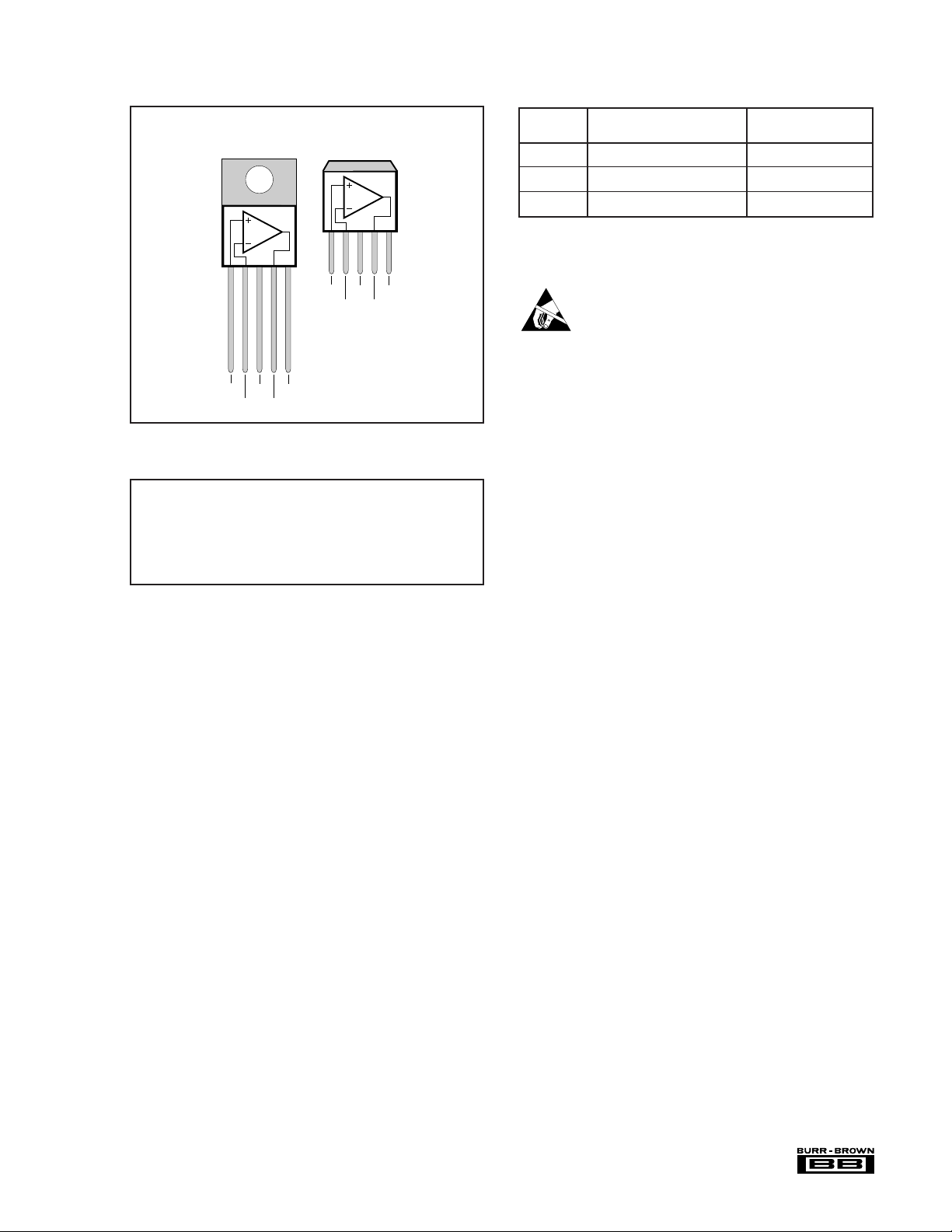
CONNECTION DIAGRAMS
PACKAGE /ORDERING INFORMATION
Top View
5-Lead TO-220
and
Stagger-Formed
TO-220
Tab is connected
to V– supply.
1234
+
V
IN
5
V–
V+
–
V
V
IN
O
Tab is connected
to V– supply.
1234
+
V
IN
5
V–
V+
–
V
V
IN
O
5-Lead
Surface Mount
ABSOLUTE MAXIMUM RATINGS
Supply Voltage, V+ to V– ................................................................... 70V
Output Current ................................................................. See SOA Curve
Input Voltage .................................................... (V–) –0.7V to (V+) +0.7V
Operating Temperature ................................................. –40°C to +125°C
Storage Temperature ..................................................... –40°C to +125°C
Junction Temperature...................................................................... 150°C
Lead Temperature (soldering –10s)
NOTE: (1) Vapor-phase or IR reflow techniques are recommended for soldering the OPA544F surface mount package. Wave soldering is not recommended
due to excessive thermal shock and “shadowing” of nearby devices.
(1)
...............................................................
300°C
PRODUCT PACKAGE NUMBER
PACKAGE DRAWING
OPA544T 5-Lead TO-220 315
OPA544T-1 5-Lead Stagger-Formed TO-220 323
OPA544F 5-Lead Surface-Mount 325
NOTE: (1) For detailed drawing and dimension table, please see end of data
sheet, or Appendix C of Burr-Brown IC Data Book.
(1)
ELECTROSTATIC
DISCHARGE SENSITIVITY
This integrated circuit can be damaged by ESD. Burr-Brown
recommends that all integrated circuits be handled with
appropriate precautions. Failure to observe proper handling
and installation procedures can cause damage.
ESD damage can range from subtle performance degradation to complete device failure. Precision integrated circuits
may be more susceptible to damage because very small
parametric changes could cause the device not to meet its
published specifications.
®
3
OPA544
 Loading...