

Burr Brown OPA4658U, OPA4658U-2K5 Datasheet
1
®
OPA4658
FEATURES
● GAIN BANDWIDTH: 900MHz at G = 2
● GAIN OF 2 STABLE
● LOW POWER: 50mW PER AMP
● LOW DIFF GAIN/PHASE ERRORS:
0.015%/0.02
°
● HIGH SLEW RATE: 1700V/µs
● PACKAGE: 14-Pin DIP and SO-14
Quad Wideband, Low Power Current Feedback
OPERATIONAL AMPLIFIER
APPLICATIONS
● MEDICAL IMAGING
● HIGH-RESOLUTION VIDEO
● HIGH-SPEED SIGNAL PROCESSING
● COMMUNICATIONS
● PULSE AMPLIFIERS
● ADC/DAC GAIN AMPLIFIER
● MONITOR PREAMPLIFIER
● CCD IMAGING AMPLIFIER
DESCRIPTION
The OPA4658 is a quad ultra-wideband, low power
current feedback video operational amplifier featuring
high slew rate and low differential gain/phase error.
The current feedback design allows for superior large
signal bandwidth, even at high gains. The low differential gain/phase errors, wide bandwidth and low
quiescent current make the OPA4658 a perfect choice
for numerous video, imaging and communications
applications.
The OPA4658 is internally compensated for stability in
gains of 2 or greater. The OPA4658 is also available in
dual (OPA2658) and single (OPA658) configurations.
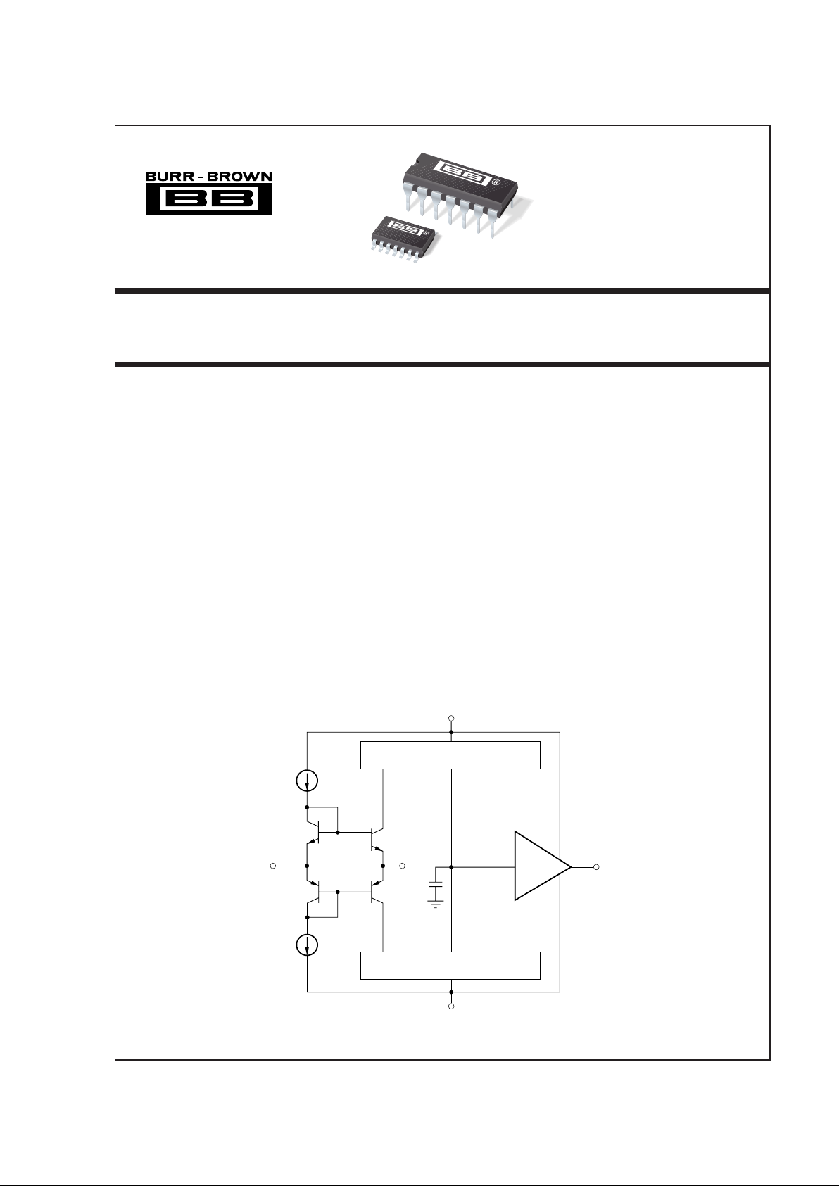
C
COMP
Current Mirror
V
–
V
+
V
OUT
I
BIAS
I
BIAS
+V
S
–V
S
Current Mirror
Buffer
OPA4658
OPA4658
OPA4658
NOTE: Diagram reflects only one-fourth of the OPA4658.
®
International Airport Industrial Park • Mailing Address: PO Box 11400, Tucson, AZ 85734 • Street Address: 6730 S. Tucson Blvd., Tucson, AZ 85706 • Tel: (520) 746-1111 • Twx: 910-952-1111
Internet: http://www.burr-brown.com/ • FAXLine: (800) 548-6133 (US/Canada Only) • Cable: BBRCORP • Telex: 066-6491 • FAX: (520) 889-1510 • Immediate Product Info: (800) 548-6132
© 1994 Burr-Brown Corporation PDS-1270C Printed in U.S.A. March, 1998

2
®
OPA4658
FREQUENCY RESPONSE
Closed-Loop Bandwidth
(2)
G = +2 450 ✻
(1)
MHz
G = +5 195 ✻ MHz
G = +10 130 ✻ MHz
Slew Rate
(3)
G = +2, 2V Step 1700 1000 ✻ V/µs
At Minimum Specified Temperature 1500 900 ✻ V/µs
Settling Time: 0.01% G = +2, 2V Step 20 ✻ ns
0.1% G = +2, 2V Step 15.1 ✻ ns
1% G = +2, 2V Step 4.8 ✻ ns
Spurious Free Dynamic Range f = 5MHz, G = +2, V
O
= 2Vp-p 66 ✻ dBc
f = 20MHz, G = +2, V
O
= 2Vp-p 57 ✻ dBc
Third-Order Intercept Point f = 10MHz 38 ✻ dBm
Differential Gain G = +2, NTSC, V
O
= 1.4Vp-p, RL = 150Ω 0.015 ✻ %
Differential Phase G = +2, NTSC, V
O
= 1.4Vp-p, RL = 150Ω 0.02 ✻ degrees
Crosstalk Input Referred, 5MHz, Three Active Channels –74 ✻ dB
Input Referred, 5MHz, Channel-to-Channel –85 ✻ dB
OFFSET VOLTAGE
Input Offset Voltage ±1.5 ±5.5 ±2 ±5mV
Over Temperature ±5 ±8 ±4 ±8mV
Power Supply Rejection V
S
= ±4.5 to ±5.5V 55 70 58 75 dB
INPUT BIAS CURRENT
Non-Inverting V
CM
= 0V ±6.5 ±30 ✻ ±18 µA
Over Temperature ±10 ±80 ✻ ±35 µA
Inverting V
CM
= 0V ±1.1 ±35 ✻✻ µA
Over Temperature ±30 ±75 ✻✻ µA
NOISE
Input Voltage Noise Density
f = 100Hz 16 ✻ nV/√Hz
f = 10kHz 3.6 ✻ nV/√Hz
f = 1MHz 3.2 ✻ nV/√Hz
f
B
= 100Hz to 200MHz 45 ✻ µVrms
Inverting Input Bias Current
Noise Density: f = 10MHz 32 ✻ pA/√Hz
Non-Inverting Input Current
Noise Density: f = 10MHz 12 ✻ pA/√Hz
Noise Figure (NF) R
S
= 100Ω 9.5 ✻ dBm
R
S
= 50Ω 11 ✻ dBm
INPUT VOLTAGE RANGE
Common-Mode Input Range ±2.9 ✻ V
Over Temperature ±2.5 ✻ V
Common-Mode Rejection V
CM
= ±1V 45 52 ✻✻ dB
INPUT IMPEDANCE
Non-Inverting 500 || 1 ✻ kΩ ||pF
Inverting 25 ✻ Ω
OPEN-LOOP TRANSIMPEDANCE
Open-Loop Transimpedance V
O
= ±2V, RL = 100Ω 150 350 200 360 kΩ
Over Temperature V
O
= ±2V, RL = 100Ω 100 290 150 300 kΩ
OUTPUT
Voltage Output No Load ±2.7 ±3.0 ✻✻ V
Over Temperature ±2.5 ±2.75 ✻✻ V
Voltage Output R
L
= 250Ω±2.7 ±3.0 ✻✻ V
Over Temperature ±2.5 ±2.7 ✻✻ V
Voltage Output R
L
= 100Ω±2.2 ±2.7 ✻✻ V
Over Temperature ±2.0 ±2.5 ✻✻ V
Output Current, Sourcing 80 120 ✻✻ mA
Over Temperature Range 70 ✻ mA
Output Current, Sinking 60 80 ✻✻ mA
Over Temperature Range 35 ✻ mA
Short Circuit Current 150 ✻ mA
Output Resistance 1MHz, G = +2 0.1 ✻ Ω
POWER SUPPLY
Specified Operating Voltage ±5 ✻ V
Operating Voltage Range ±4.5 ±5.5 ✻✻V
Quiescent Current All Channels, V
S
= ±5V ±19 ±31 ±13 ±20 ±23 mA
Over Temperature ±20 ±34 ±21 ±26 mA
TEMPERATURE RANGE
Specification: P, U, UB –40 +85 ✻✻°C
Thermal Resistance,
θ
JA
P 75 ✻ °C/W
U 75 ✻ °C/W
SPECIFICATIONS
OPA4658P, U OPA4658UB
PARAMETER CONDITION MIN TYP MAX MIN TYP MAX UNITS
At T
A
= +25°C, VS = ±5V, RL = 100Ω, CL = 2pF, RFB = 402Ω, unless otherwise noted.
NOTES: (1) An asterisk (✻) specifies the same value as the grade to the left. (2) Bandwidth can be affected by a non-optimal PC board layout. Refer to the
demonstration board layout for details. (3) Slew rate is rate of change from 10% to 90% of output voltage step.
3
®
OPA4658
1
2
3
4
5
6
7
14
13
12
11
10
9
8
Output 4
–Input 4
+Input 4
–V
S
+Input 3
–Input 3
Output 3
Output 1
–Input 1
+Input 1
+V
S
+Input 2
–Input 2
Output 2
ABSOLUTE MAXIMUM RATINGS
Supply ..........................................................................................±5.5VDC
Internal Power Dissipation
(1)
.......................See Applications Information
Differential Input Voltage .............................................................. Total V
S
Input Voltage Range .................................... See Applications Information
Storage Temperature Range: P, U, UB........................ –40°C to +125°C
Lead Temperature (soldering, 10s).............................................. +300°C
(soldering, SOIC 3s) ...................................................................... +260°C
Junction Temperature (T
J
) ............................................................ +175°C
NOTE: (1) Packages must be derated based on specified
θ
JA
. Maximum
T
J
must be observed.
PACKAGE INFORMATION
PACKAGE DRAWING
PRODUCT PACKAGE NUMBER
(1)
OPA4658P 14-Pin Plastic DIP 010
OPA4658U, UB SO-14 Surface Mount 235
NOTE: (1) For detailed drawing and dimension table, please see end of data
sheet, or Appendix C of Burr-Brown IC Data Book.
PIN CONFIGURATION
Top View DIP/SO-14
ORDERING INFORMATION
(1)
PRODUCT PACKAGE TEMPERATURE RANGE
OPA4658P 14-Pin Plastic DIP –40°C to +85°C
OPA4658U, UB SO-14 Surface Mount –40°C to +85°C
NOTE: (1) The "B" grade of the SOIC package will be marked with a "B" by pin 8.
Refer to mechanical section for the location.
ELECTROSTATIC
DISCHARGE SENSITIVITY
This integrated circuit can be damaged by ESD. Burr-Brown
recommends that all integrated circuits be handled with
appropriate precautions. Failure to observe proper handling
and installation procedures can cause damage.
ESD damage can range from subtle performance degradation
to complete device failure. Precision integrated circuits may
be more susceptible to damage because very small parametric
changes could cause the device not to meet its published
specifications.
The information provided herein is believed to be reliable; however, BURR-BROWN assumes no responsibility for inaccuracies or omissions. BURR-BROWN assumes
no responsibility for the use of this information, and all use of such information shall be entirely at the user’s own risk. Prices and specifications are subject to change
without notice. No patent rights or licenses to any of the circuits described herein are implied or granted to any third party. BURR-BROWN does not authorize or warrant
any BURR-BROWN product for use in life support devices and/or systems.
4
®
OPA4658
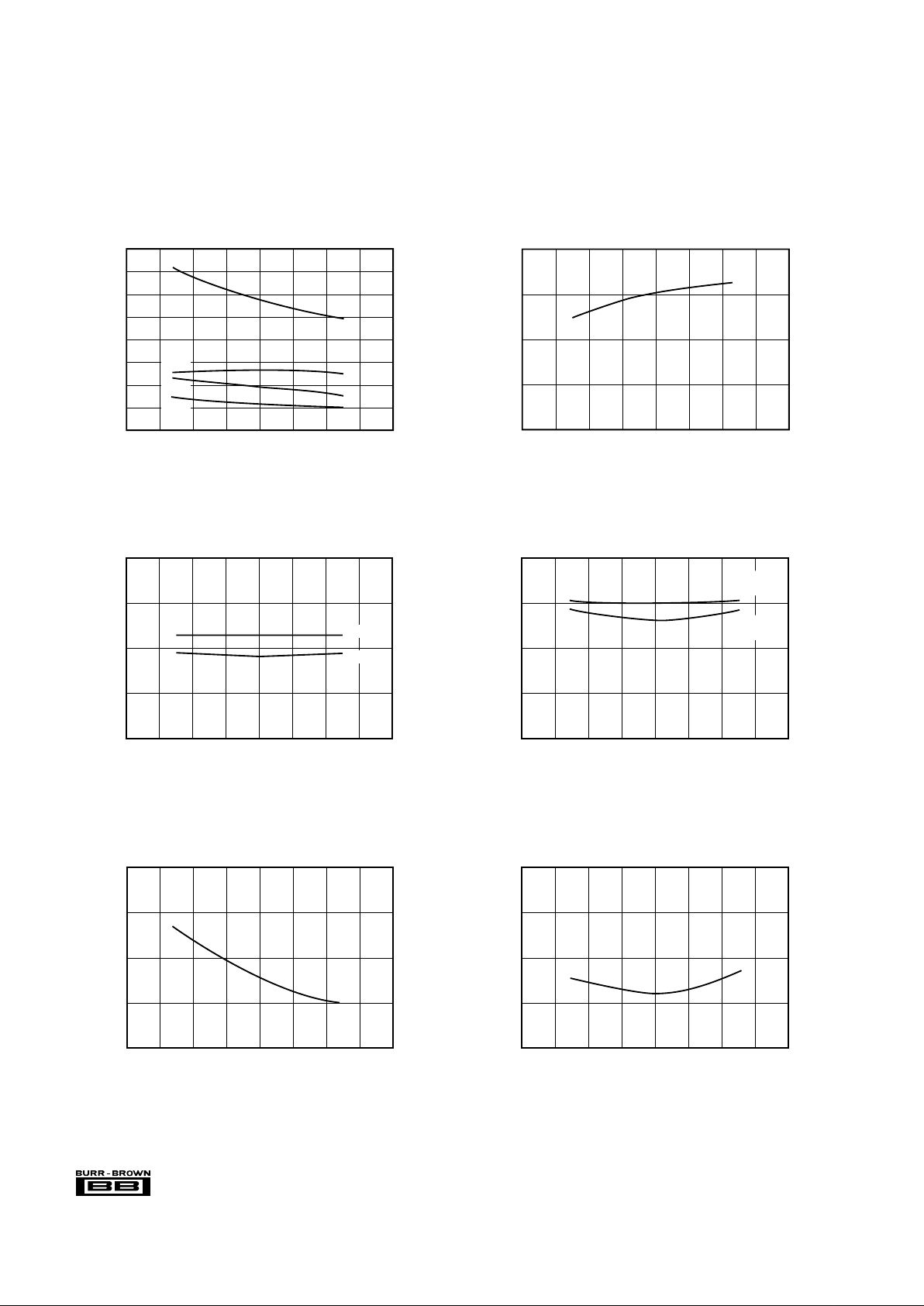
TYPICAL PERFORMANCE CURVES
At TA = +25°C, VS = ±5V, RL = 100Ω, CL = 2pF, RFB = 402Ω, unless otherwise noted.
OUTPUT CURRENT vs TEMPERATURE
60
55
50
45
40
–75 –50 –25 0 25 50 75 100 125
Output Current (mA)
Temperature (°C)
IO+
I
O
–
NON-INVERTING INPUT BIAS CURRENT
vs TEMPERATURE
10
8
6
4
2
–75 –50 –25 0 25 50 75 100 125
Non-Inverting Input Bias Current I
B
+ (µA)
Temperature (°C)
OUTPUT SWING vs TEMPERATURE
4
3
2
1
0
–75 –50 –25 0 25 50 75 100 125
Output Swing (V)
Temperature (°C)
±V
O
RL = 250Ω
±V
O
RL = 100Ω
INVERTING INPUT BIAS CURRENT
vs TEMPERATURE
8
6
4
2
0
–75 –50 –25 0 25 50 75 100 125
Inverting Input Bias Current I
B
– (µA)
Temperature (°C)
PSRR AND CMRR vs TEMPERATURE
85
80
75
70
65
60
55
50
45
–75 –50 –25 0 25 50 75 100 125
PSRR , CMRR (dB)
Temperature (°C)
PSRR
PSR+
PSR–
CMRR
SUPPLY CURRENT vs TEMPERATURE
(Total of All Four Op Amps)
21
20
19
18
17
–75 –50 –25 0 25 50 75 100 125
Supply Current (±mA)
Temperature (°C)
5
®
OPA4658
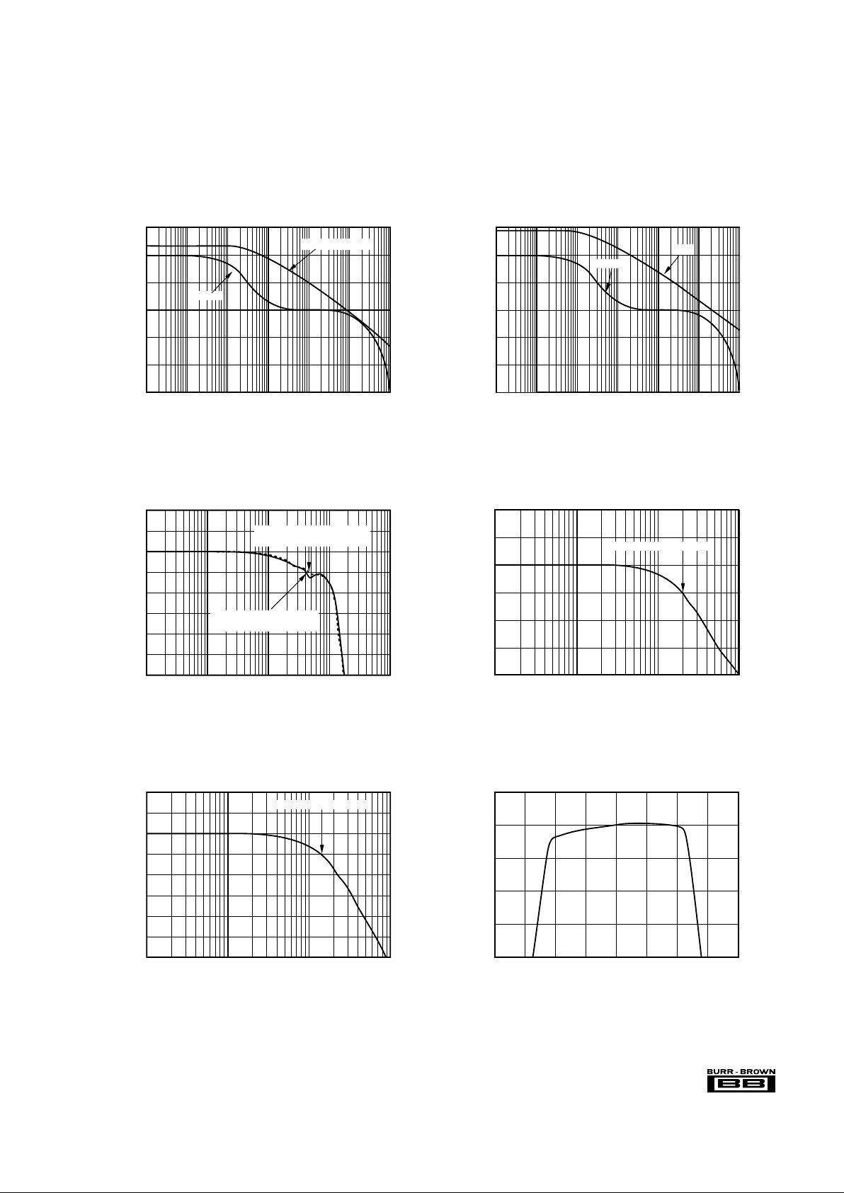
TYPICAL PERFORMANCE CURVES (CONT)
At TA = +25°C, VS = ±5V, RL = 100Ω, CL = 2pF, RFB = 402Ω, unless otherwise noted.
OPEN-LOOP GAIN AND PHASE vs FREQUENCY
Frequency (Hz)
60
40
20
0
–20
–40
–60
0
–45
–90
–135
–180
–225
1k 10k 100k 1M 10M 100M 1G
Open-Loop Gain (dB)
Open-Loop Phase (°)
Gain
Phase
COMMON-MODE REJECTION
vs INPUT COMMON-MODE VOLTAGE
55
50
45
40
35
30
–4–3–2–101234
Common-Mode Rejection (dB)
Common-Mode Voltage (V)
CLOSED-LOOP BANDWIDTH (G = +5)
Frequency (Hz)
20
17
14
11
8
5
2
1M 10M 100M 1G
Bandwidth = 205MHz
Gain (dB)
10
6
10
5
10
4
10
3
10
2
10
1
1
0
–45
–90
–135
–180
–225
1k 10k 100k 1M 10M 100M 1G
OPEN-LOOP TRANSIMPEDANCE AND PHASE
vs FREQUENCY
Frequency (Hz)
Transimpedance (Ω)
Open-Loop Phase (°)
Phase
Transimpedance
CLOSED-LOOP BANDWIDTH (G = +10)
Frequency (Hz)
26
23
20
17
14
11
8
5
2
1M 10M 100M 1G
Gain (dB)
Bandwidth = 134MHz
CLOSED-LOOP BANDWIDTH (G = +2)
Frequency (Hz)
12
9
6
3
0
–3
–6
–9
–12
1M 10M 100M 1G 10G
Gain (dB)
SO-14 Bandwidth = 458MHz
(Dashed Line)
DIP Bandwidth = 435M
(Solid Line)
 Loading...