

Page 1
查询OPA4650供应商查询OPA4650供应商
®
OPA4650
OPA4650
OPA4650
DEMO BOARD
AVAILABLE
Wideband, Low Power, Quad Voltage Feedback
OPERATIONAL AMPLIFIER
FEATURES
● LOW POWER: 50mW/channel
● UNITY GAIN STABLE BANDWIDTH:
360MHz
● FAST SETTLING TIME: 20ns to 0.01%
● LOW INPUT BIAS CURRENT: 5
µA
● DIFFERENTIAL GAIN/PHASE ERROR:
0.01%/0.025
°
● 14-PIN DIP and SO-14 SURFACE MOUNT
PACKAGES AVAILABLE
APPLICATIONS
● HIGH RESOLUTION VIDEO
● MONITOR PREAMPLIFIER
● CCD IMAGING AMPLIFIER
● ULTRASOUND SIGNAL PROCESSING
● ADC/DAC BUFFER AMPLIFIER
● ACTIVE FILTERS
● HIGH SPEED INTEGRATORS
● DIFFERENTIAL AMPLIFIER
DESCRIPTION
The OPA4650 is a quad, low power, wideband voltage
feedback operational amplifier. It features a high bandwidth of 360MHz as well as a 12-bit settling time of
only 20ns. The low input bias current allows its use in
high speed integrator applications, while the wide
bandwidth and true differential input stage make it
suitable for use in a variety of active filter applications. Its low distortion gives exceptional performance
for telecommunications, medical imaging and video
applications.
The OPA4650 is internally compensated for unitygain stability. This amplifier has a fully symmetrical
differential input due to its “classical” operational
amplifier circuit architecture. Its unusual combination
of speed, accuracy and low power make it an outstanding choice for many portable, multi-channel and other
high speed applications, where power is at a premium.
The OPA4650 is also available in single (OPA650)
and dual (OPA2650) configurations.
+V
S
Non-Inverting
Input
Output
Inverting
Input
International Airport Industrial Park • Mailing Address: PO Box 11400, Tucson, AZ 85734 • Street Address: 6730 S. Tucson Blvd., Tucson, AZ 85706 • Tel: (520) 746-1111 • Twx: 910-952-1111
Internet: http://www.burr-brown.com/ • FAXLine: (800) 548-6133 (US/Canada Only) • Cable: BBRCORP • Telex: 066-6491 • FAX: (520) 889-1510 • Immediate Product Info: (800) 548-6132
© 1994 Burr-Brown Corporation PDS-1267B Printed in U.S.A. July, 1995
Current
Mirror
–V
S
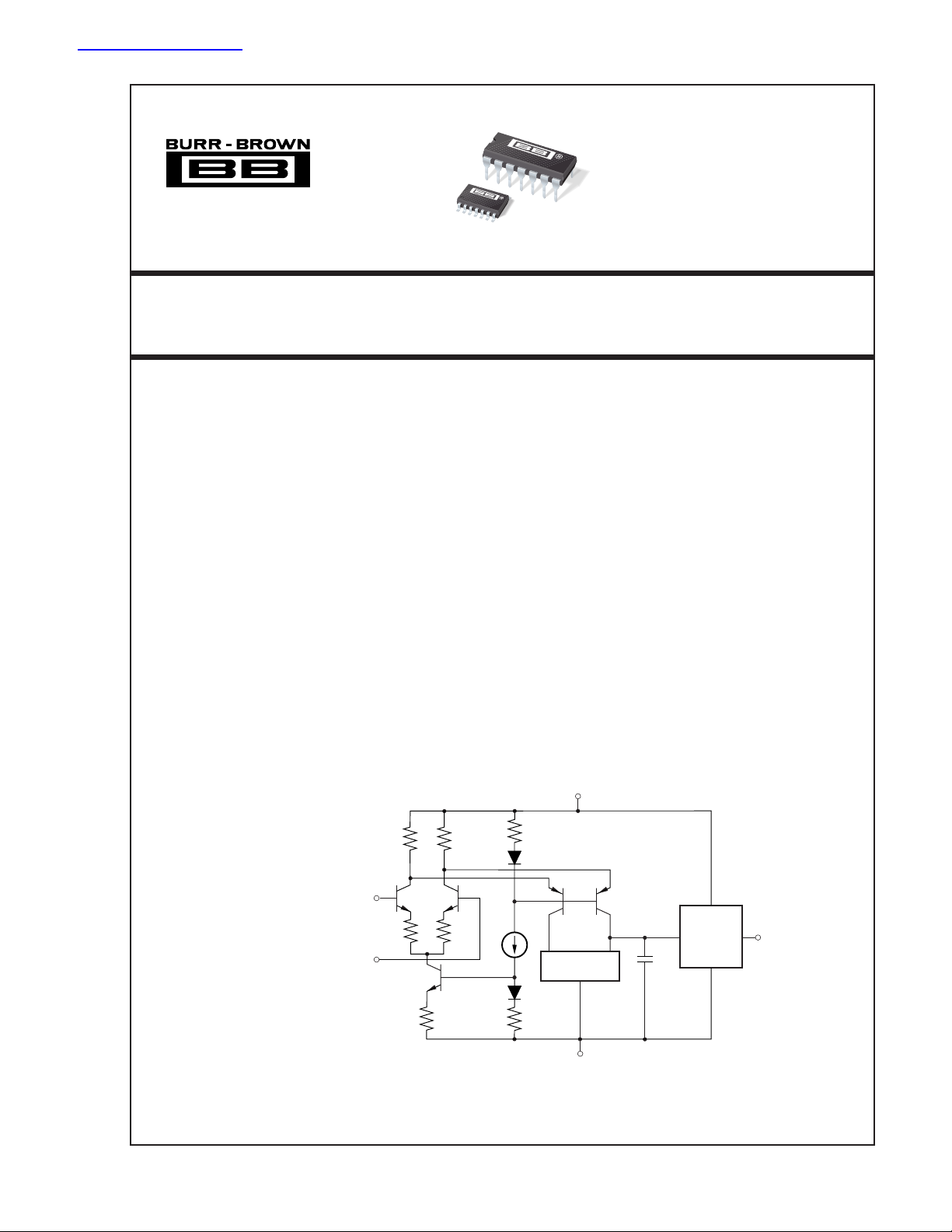
Simplified Schematic
1 of 4 Channels
Stage
C
C
Output
Page 2
SPECIFICATIONS
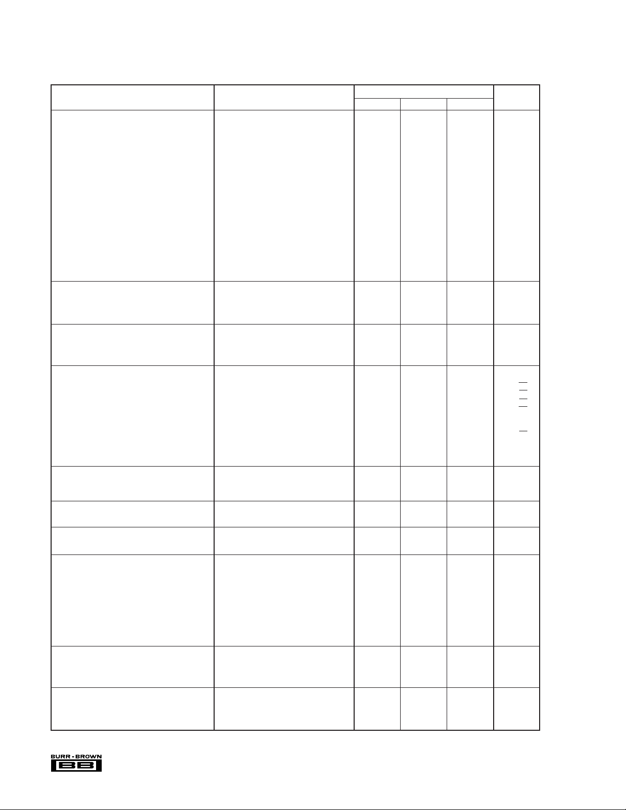
At TA = +25°C, VS = ±5V, RL = 100Ω, and RFB = 402Ω, unless otherwise noted. RFB = 25Ω for a gain of +1.
OPA4650P, U
PARAMETER CONDITIONS MIN TYP MAX UNITS
FREQUENCY RESPONSE
Closed-Loop Bandwidth
Gain Bandwidth Product 160 MHz
Slew Rate
Rise Time 0.2V Step 1 ns
Fall Time 0.2V Step 1 ns
Settling Time 0.01% G = +1, 2V Step 20 ns
(2)
Over Specified Temperature 220 V/µs
Spurious Free Dynamic Range G = +1, f = 5.0 MHz, V
Differential Gain G = +2, NTSC, V
Differential Phase G = +2, NTSC, V
Bandwidth for 0.1dB Flatness G = +2 21 MHz
Crosstalk Input Referred, 5MHz, all hostile –63 dB
OFFSET VOLTAGE
Input Offset Voltage ±1 ±5.5 mV
Average Drift ±3 µV/°C
Power Supply Rejection (+V
INPUT BIAS CURRENT
Input Bias Current V
Over Temperature 30 µA
Input Offset Current V
Over Temperature 3.0 µA
INPUT NOISE
Input Voltage Noise
Noise Density, f = 100Hz 43 nV/√Hz
Integrated Noise, BW = 10Hz to 100MHz 84 µVp-p
Input Bias Current Noise
Current Noise Density, f = 0.1MHz to 100MHz 1.2 pA/√Hz
Noise Figure (NF)
INPUT VOLTAGE RANGE
Common-Mode Input Range ±2.8 V
Over Specified Temperature ±2.2 V
Common-Mode Rejection V
INPUT IMPEDANCE
Differential 15 || 1 kΩ || pF
Common-Mode 16 || 1 MΩ || pF
OPEN-LOOP GAIN
Open-Loop Voltage Gain V
Over Specified Temperature V
OUTPUT
Voltage Output
Over Specified Temperature No Load ±2.2 ±3.0 V
Output Current, Sourcing 75 110 mA
Over Temperature Range 65 mA
Output Current, Sinking 65 85 mA
Over Temperature Range 35 mA
Short-Circuit Current 150 mA
Output Resistance 0.1MHz, G = +1 0.08 Ω
POWER SUPPLY
Specified Operating Voltage ±5V
Operating Voltage Range ±4.5 ±5.5 V
Quiescent Current All Channels ±23 ±32 mA
Over Specified Temperature ±35 mA
TEMPERATURE RANGE
Specification: P, U –40 +85 °C
Thermal Resistance,
NOTES: (1) Frequency response can be strongly influenced by PC board parasites. The OPA4650 is nominally compensated assuming 2pF parasitic load. The
demonstration board, DEM-OPA465xP, shows a low parasitic layout for this part. (2) Slew rate is rate of change from 10% to 90% of output voltage step.
(1)
G = +1 360 MHz
G = +2 120 MHz
G = +5 35 MHz
G = +10 16 MHz
G = +1, 2V Step 240 V/µs
0.1% G = +1, 2V Step 10.3 ns
1% G = +1, 2V Step 7.9 ns
= 100Ω 68 dBc
R
L
= 402Ω 74 dBc
R
L
O
O
= 2Vp-p
O
= 1.4Vp, RL = 150Ω 0.01 %
= 1.4Vp, RL = 150Ω 0.025 Degrees
Input Referred, 5MHz, Channel-to-Channel –66 dB
)|V
S
) 47 52 dB
(–V
S
| = 4.5V to 5.5V 60 76 dB
S
= 0V 5 20 µA
CM
= 0V 0.5 1.0 µA
CM
f = 10kHz 9.4 nV/√Hz
f = 1MHz 8.4 nV/√Hz
f = 1MHz to 100MHz 8.4 nV/√Hz
= 10kΩ 4.0 dBm
R
S
= 50Ω 19.5 dBm
R
S
= ±0.5V 65 90 dB
CM
= ±2V, RL = 100Ω 45 51 dB
O
= ±2V, RL = 100Ω 43 dB
O
R
= 250Ω±2.2 ±2.5 V
L
R
= 100Ω±2.0 ±2.3 V
L
θ
JA
P 75 °C/W
U 75 °C/W
®
OPA4650
2
Page 3
ABSOLUTE MAXIMUM RATINGS
Total Supply Voltage Across Device...................................................11V
Internal Power Dissipation ........................... See Thermal Considerations
Differential Input Voltage .................................................................. ±2.7V
Common-Mode Input Voltage Range .................................................. ±V
Storage Temperature Range: P, U, .............................. –40°C to +125°C
Lead Temperature (soldering, 10s) .............................................. +300°C
Junction Temperature (T
(soldering, SOIC 3s) ....................................... +260°C
) ............................................................ +175°C
J
PACKAGE INFORMATION
PRODUCT PACKAGE NUMBER
S
OPA4650U SO-14 Surface Mount 235
OPA4650P 14-Pin Plastic DIP 010
NOTE: (1) For detailed drawing and dimension table, please see end of data
sheet, or Appendix C of Burr-Brown IC Data Book.
PACKAGE DRAWING
(1)
ORDERING INFORMATION
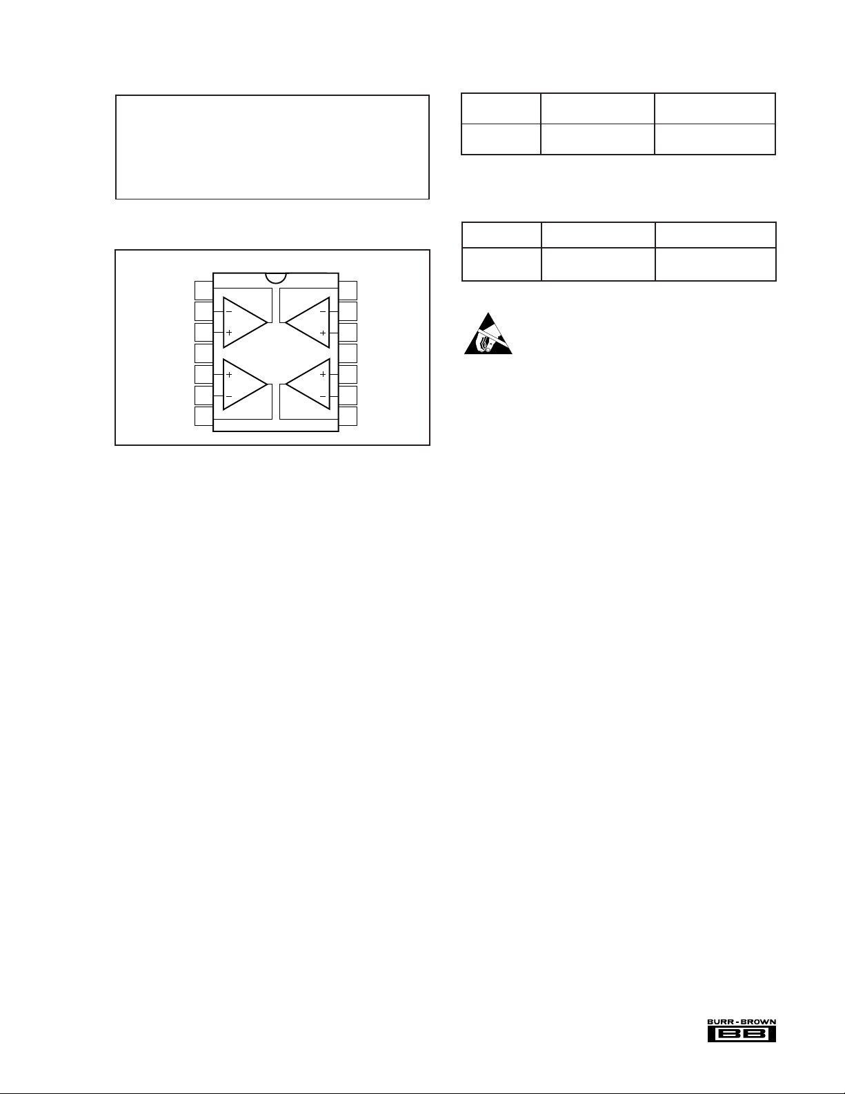
PIN CONFIGURATION
Top View DIP/SO-14
Output 1
–Input 1
+Input 1
+V
+Input 2
–Input 2
Output 2
1
2
3
4
S
5
6
7
14
13
12
11
10
9
8
Output 4
–Input 4
+Input 4
–V
+Input 3
–Input 3
Output 3
PRODUCT PACKAGE TEMPERATURE RANGE
OPA4650U SO-14 Surface Mount –40°C to +85°C
OPA4650P 14-Pin Plastic DIP –40°C to +85°C
ELECTROSTATIC
S
Electrostatic discharge can cause damage ranging from performance degradation to complete device failure. Burr-Brown
Corporation recommends that all integrated circuits be handled
and stored using appropriate ESD protection methods.
ESD damage can range from subtle performance degradation
to complete device failure. Precision integrated circuits may
be more susceptible to damage because very small parametric
changes could cause the device not to meet published specifications.
DISCHARGE SENSITIVITY
®
3
OPA4650
Page 4
TYPICAL PERFORMANCE CURVES
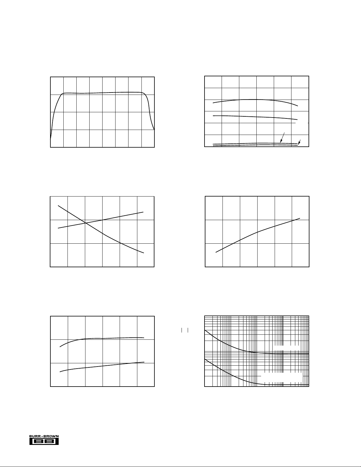
At TA = +25°C, VS = ±5V, RL = 100Ω, and RFB = 402Ω, unless otherwise noted. RFB = 25Ω for a gain of +1.
COMMON-MODE REJECTION
vs INPUT COMMON-MODE VOLTAGE
100
90
80
70
Common-Mode Rejection (dB)
60
–4 –3 –2 –1 0 1 2 3 4
Common-Mode Voltage (V)
INPUT BIAS CURRENT AND OFFSET VOLTAGE
vs TEMPERATURE
7
6
110
100
90
80
70
, PSR and CMRR (dB)
OL
A
60
50
–50 –25 0 25 50 75 125
2
V
OS
1
26
24
AOL, PSR AND CMRR vs TEMPERATURE
PSR–
Temperature (°C)
SUPPLY CURRENT vs TEMPERATURE
CMRR
PSR+
A
OL
5
Input Bias Current (mA)
4
–50 –25 0 25 50 75 100
Temperature (°C)
70
65
60
Output Current (±mA)
55
–50 –25 0 25 50 75 100
OUTPUT CURRENT vs TEMPERATURE
+
I
O
–
I
O
Temperature (°C)
0
I
B
Offset Voltage (mV)
–1
22
Supply Current (±mA)
I
Q
20
–50 –25 0 25 50 75 100
Temperature (°C)
INPUT VOLTAGE AND CURRENT NOISE
vs FREQUENCY
100
10
Input Current Noise (pA/√Hz)
Input Voltage Noise (nV/√Hz)
1
100 1k 10k 100k 1M
Voltage Noise
Non-inverting and
Inverting Current Noise
Frequency (Hz)
®
OPA4650
4
Page 5
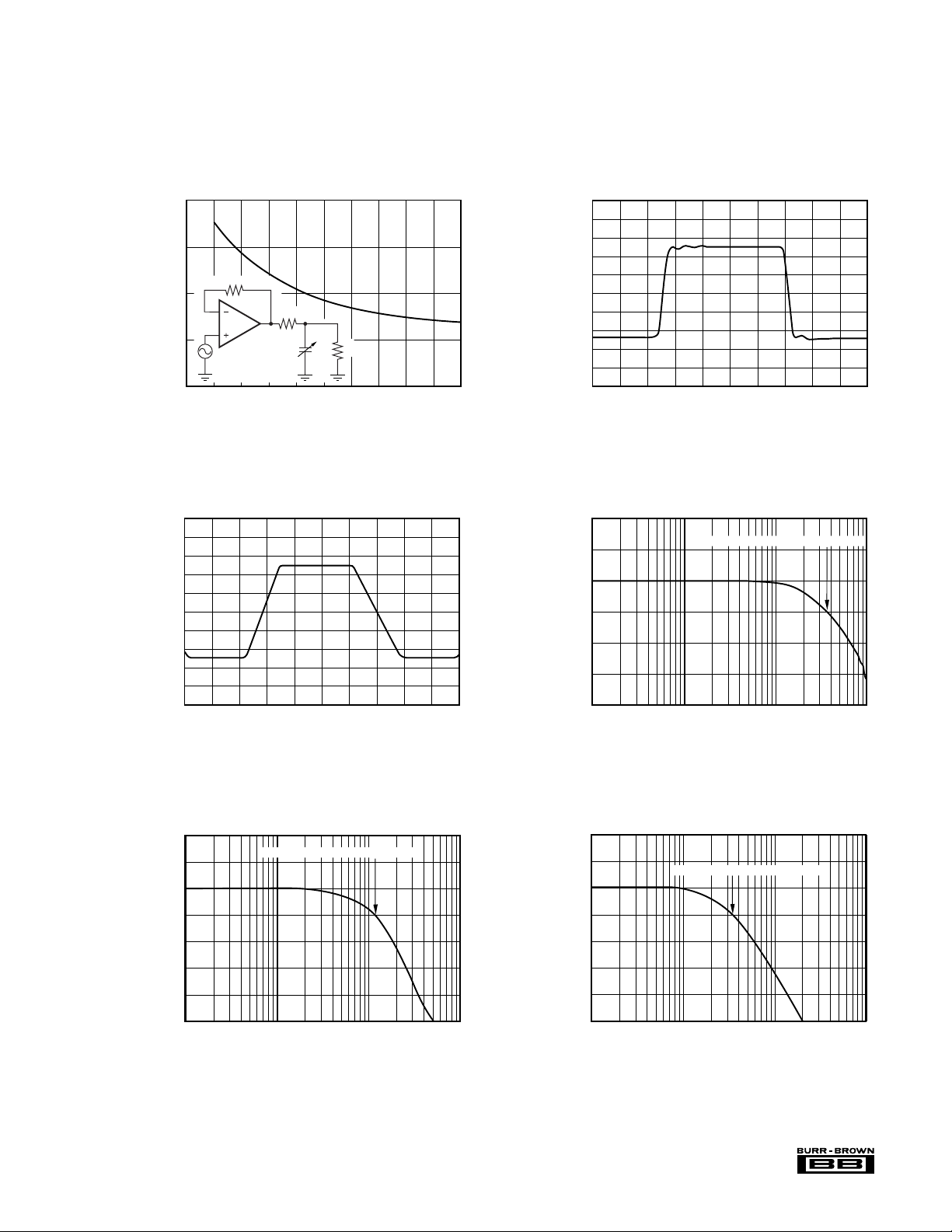
TYPICAL PERFORMANCE CURVES (CONT)
SMALL SIGNAL TRANSIENT RESPONSE
(G = +1)
Time (5ns/div)
200
160
120
80
40
0
–40
–80
–120
–160
–200
Output Voltage (mV)
CLOSED-LOOP BANDWIDTH (G = +1)
Frequency (Hz)
6
3
0
–3
–6
–9
–12
1M 10M 100M 1G
SO-14/DIP Bandwidth = 360MHz
Gain (dB)
CLOSED-LOOP BANDWIDTH (G = +5)
Frequency (Hz)
21
17
14
11
8
5
2
–1
1M 10M 100M 1G
Gain (dB)
SO-14/DIP Bandwidth = 35MHz
At TA = +25°C, VS = ±5V, RL = 100Ω, and RFB = 402Ω, unless otherwise noted. RFB = 25Ω for a gain of +1.
RECOMMENDED ISOLATION RESISTANCE
vs CAPACITIVE LOAD
40
(Ω)
30
ISO
25Ω
20
R
10
OPA4650
Isolation Resistance, R
ISO
C
1kΩ
L
0
0 20 40 60 80 100
Capacitive Load, CL (pF)
LARGE SIGNAL TRANSIENT RESPONSE
(G = +1)
2.0
1.6
1.2
0.8
0.4
0
–0.4
–0.8
Output Voltage (V)
–1.2
–1.6
–2.0
Time (5ns/div)
12
CLOSED-LOOP BANDWIDTH (G = +2)
9
SO-14/DIP Bandwidth = 120MHz
6
3
0
Gain (dB)
–3
–6
–9
1M 10M 100M 1G
Frequency (Hz)
®
5
OPA4650
Page 6
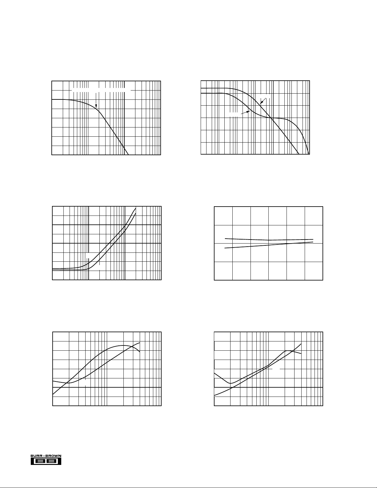
TYPICAL PERFORMANCE CURVES (CONT)
At TA = +25°C, VS = ±5V, RL = 100Ω, and RFB = 402Ω, unless otherwise noted. RFB = 25Ω for a gain of +1.
26
23
20
17
14
Gain (dB)
11
8
5
2
1M 10M 100M 1G
CLOSED-LOOP BANDWIDTH (G = +10)
SO-14/DIP Bandwidth = 16MHz
Frequency (Hz)
60
50
40
30
Gain (dB)
20
10
0
1k 10k 100k 1M 10M 100M 1G
OPEN-LOOP GAIN AND PHASE
vs FREQUENCY
Gain
Phase
Frequency (Hz)
+45
0
–45
–90
Phase (°)
–135
–180
HARMONIC DISTORTION vs FREQUENCY
–50
(G = +1, V
= 2Vp-p)
O
–60
–70
3f
–80
Harmonic Distortion (dBc)
O
2f
O
–90
100k 1M 10M 100M
Frequency (Hz)
5MHz HARMONIC DISTORTION
vs OUTPUT SWING
–60
G = +2
–70
–80
–90
Harmonic Distortion (dBc)
3f
O
2f
O
HARMONIC DISTORTION vs TEMPERATURE
= 5MHz, G = +1, VO = 2Vp-p)
(f
–50
O
–60
3f
O
–70
2f
O
–80
Harmonic Distortion (dB)
–90
–50 –25 0 25 50 75 100
Temperature (°C)
10MHz HARMONIC DISTORTION
vs OUTPUT SWING
–50
–60
–70
–80
Harmonic Distortion (dBc)
3f
O
2f
O
–100
0.1 1 10
Output Swing (Vp-p)
®
OPA4650
–90
0.1 1 10
Output Swing (Vp-p)
6
Page 7
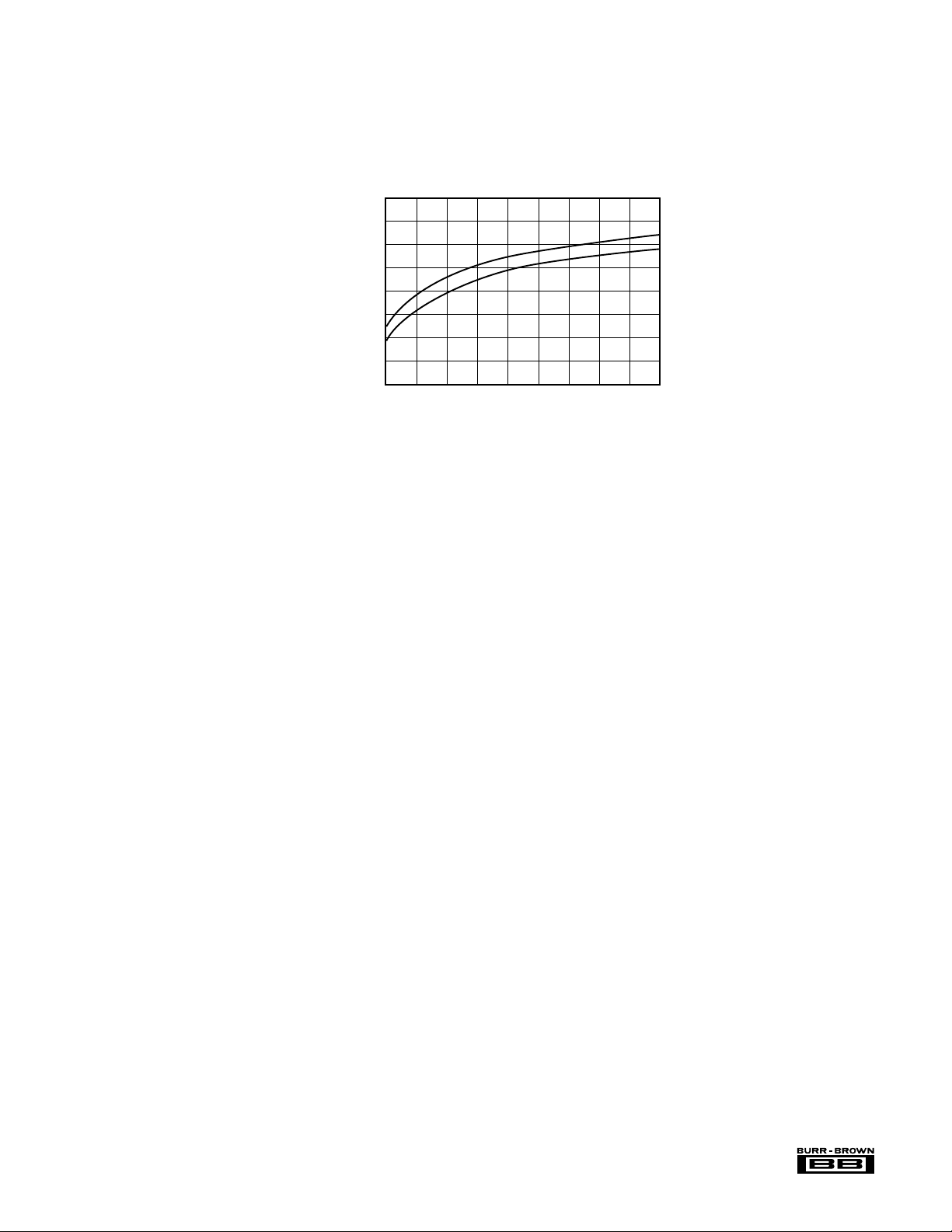
TYPICAL PERFORMANCE CURVES (CONT)
At TA = +25°C, VS = ±5V, RL = 100Ω, and RFB = 402Ω, unless otherwise noted. RFB = 25Ω for a gain of +1.
HARMONIC DISTORTION vs GAIN
= 5MHz, VO = 2Vp-p)
(f
40
O
50
60
70
Harmonic Distortion (dBc)
80
12345678910
3f
O
2f
O
Non-Inverting Gain (V/V)
®
7
OPA4650
Page 8

DISCUSSION OF
PERFORMANCE
The OPA4650 is a quad low power, wideband voltage
feedback operational amplifier. Each channel is internally
compensated to provide unity gain stability. The OPA4650’s
voltage feedback architecture features true differential and
fully symmetrical inputs. This minimizes offset errors, making the OPA4650 well suited for implementing filter and
instrumentation designs. As a quad operational amplifier,
OPA4650 is an ideal choice for designs requiring multiple
channels where reduction of board space, power dissipation
and cost are critical. Its ac performance is optimized to
provide a gain bandwidth product of 160MHz and a fast
0.1% settling time of 10.3ns, which is an important consideration in high speed data conversion applications. Along
with its excellent settling characteristics, the low dc input
offset of ±1mV and drift of ±3µV/°C support high accuracy
requirements. In applications requiring a higher slew rate
and wider bandwidth, such as video and high bit rate digital
communications, consider the quad current feedback
OPA4658.
CIRCUIT LAYOUT AND BASIC OPERATION
Achieving optimum performance with a high frequency amplifier like the OPA4650 requires careful attention to layout
parasitics and selection of external components. Recommendations for PC board layout and component selection include:
a) Minimize parasitic capacitance to any ac ground for all
of the signal I/O pins. Parasitic capacitance on the output
and inverting input pins can cause instability; on the noninverting input it can react with the source impedance to
cause unintentional bandlimiting. To reduce unwanted capacitance, a window around the signal I/O pins should be
opened in all of the ground and power planes. Otherwise,
ground and power planes should be unbroken elsewhere on
the board.
b) Minimize the distance (< 0.25") from the two power pins
to high frequency 0.1µF decoupling capacitors. At the pins,
the ground and power plane layout should not be in close
proximity to the signal I/O pins. Avoid narrow power and
ground traces to minimize inductance between the pins and
the decoupling capacitors. Larger (2.2µF to 6.8µF) decoupling
capacitors, effective at lower frequencies, should also be
used. These may be placed somewhat farther from the
device and may be shared among several devices in the same
area of the PC board.
c) Careful selection and placement of external components will preserve the high frequency performance of the
OPA4650. Resistors should be a very low reactance type.
Surface mount resistors work best and allow a tighter overall
layout. Metal film or carbon composition axially-leaded
resistors can also provide good high frequency performance.
Again, keep their leads as short as possible. Never use
wirewound type resistors in a high frequency application.
Since the output pin and the inverting input pin are most
sensitive to parasitic capacitance, always position the feedback and series output resistor, if any, as close as possible to
®
OPA4650
the package pins. Surface mount feedback resistors directly
adjacent to the output and inverting input pins work well for
the quad pinout. Other network components, such as noninverting input termination resistors, should also be placed
close to the package.
Even with a low parasitic capacitance shunting the resistor,
excessively high resistor values can create significant time
constants and degrade performance. Good metal film or
surface mount resistors have approximately 0.2pF in shunt
with the resistor. For resistor values > 1.5kΩ, this adds a
pole and/or zero below 500MHz that can affect circuit
operation. Keep resistor values as low as possible consistent
with output loading considerations. The 402Ω feedback
used for the Typical Performance Plots is a good starting
point for design. Note that a 25Ω feedback resistor, rather
than a direct short, is suggested for a unity gain follower.
This effectively reduces the Q of what would otherwise be
a parasitic inductance (the feedback wire) into the parasitic
capacitance at the inverting input.
d) Connections to other wideband devices on the board
may be made with short direct traces or through on-board
transmission lines. For short connections, consider the trace
and the input to the next device as a lumped capacitive load.
Relatively wide traces (50 to 100 mils) should be used,
preferably with ground and power planes opened up around
them. Estimate the total capacitive load and set R
the plot of recommended R
parasitic loads may not need an R
vs capacitive load. Low
ISO
since the OPA4650 is
ISO
nominally compensated to operate with a 2pF parasitic load.
If a long trace is required and the 6dB signal loss intrinsic to
doubly terminated transmission lines is acceptable, implement a matched impedance transmission line using microstrip
or stripline techniques (consult an ECL design handbook for
microstrip and stripline layout techniques). A 50Ω environment is not necessary on board, and in fact a higher impedance environment will improve distortion as shown in the
distortion vs load plot. With a characteristic impedance
defined based on board material and desired trace dimensions, a matching series resistor into the trace from the
output of the amplifier is used as well as a terminating shunt
resistor at the input of the destination device. Remember
also that the terminating impedance will be the parallel
combination of the shunt resistor and the input impedance of
the destination device; the total effective impedance should
match the trace impedance. Multiple destination devices are
best handled as separate transmission lines, each with their
own series and shunt terminations.
If the 6dB attenuation loss of a doubly terminated line is
unacceptable, a long trace can be series-terminated at the
source end only. This will help isolate the line capacitance
from the op amp output, but will not preserve signal integrity
as well as a doubly terminated line. If the shunt impedance
at the destination end is finite, there will be some signal
attenuation due to the voltage divider formed by the series
and shunt impedances.
e) Socketing a high speed part like the OPA4650 is not
recommended. The additional lead length and pin-to-pin
capacitance introduced by the socket creates an extremely
troublesome parasitic network which can make it almost
8
ISO
from
Page 9
SMALL-SIGNAL OUTPUT IMPEDANCE
vs FREQUENCY
Frequency (Hz)
1k
100
10
1
0.1
0.01
10k 100k 1M 100M10M
Output Impedance (Ω)
G = +1
R
2
OPA4650
R3 = R1 || R
2
(1)
R
1
R
TRIM
+V
s
–V
S
20kΩ
VIN or Ground
Output Trim Range +V
S
to –V
S
NOTE: (1) R3 is optional and can be used to cancel offset errors
due to input bias currents.
≅
R
TRIM
47kΩ
R
2
R
2
R
TRIM
0.1µF
impossible to achieve a smooth, stable response. Best results
are obtained by soldering the part onto the board. If socketing for the DIP package is desired, high frequency flush
mount pins (e.g., McKenzie Technology #710C) can give
good results.
The OPA4650 is nominally specified for operation using ±5V
power supplies. A 10% tolerance on the supplies, or an ECL
–5.2V for the negative supply, is within the maximum specified total supply voltage of 11V. Higher supply voltages can
break down internal junctions possibly leading to catastrophic
failure. Single supply operation is possible as long as common mode voltage constraints are observed. The common
mode input and output voltage specifications can be interpreted as a required headroom to the supply voltage. Observing this input and output headroom requirement will allow
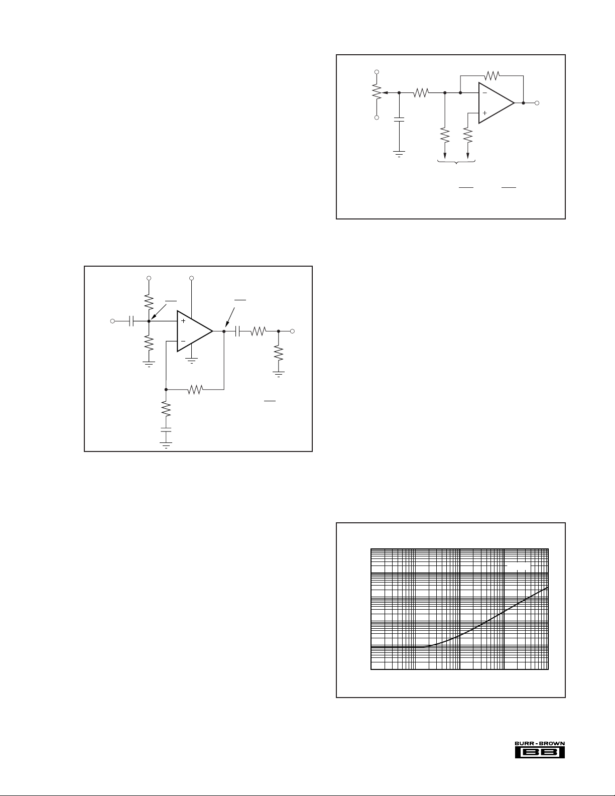
non-standard or single supply operation. Figure 1 shows one
approach to single-supply operation.
+V
S
V
AC
V
2
S
R
402Ω
+V
S
1/4
OPA4650
R
F
402Ω
G
V
OUT
V
S
= + AV V
2
R
OUT
AV = 1 +
AC
R
L
R
F
R
G
FIGURE 2. Offset Voltage Trim.
OPA4650. ESD damage can cause subtle changes in amplifier input characteristics without necessarily destroying the
device. In precision operational amplifiers, this may cause a
noticeable degradation of offset voltage and drift. ESD
handling precautions are strongly recommended when handling the OPA4650.
OUTPUT DRIVE CAPABILITY
The OPA4650 has been optimized to drive 75Ω and 100Ω
resistive loads. The device can drive 1Vp-p into a 75Ω
load. This high output drive capability makes the OPA4650
an ideal choice for a wide range of RF, IF and video
applications. In many cases, additional buffer amplifiers
are unnecessary.
Many demanding high speed applications, such as driving
Analog-to-Digital converters, require op amps with low
wideband output impedance. For example, low output imped-
FIGURE 1. Single Supply Operation.
ance is essential when driving the signal-dependent capacitance at the input of a flash A/D converter. As shown in
OFFSET VOLTAGE ADJUSTMENT
One simple way to null the initial offset voltage while
Figure 3, the OPA4650 maintains very low closed-loop
output impedance over frequency. Closed-loop output impedance increases with frequency since loop gain is decreasing.
retaining the low offset drift of the OPA4650 is shown in
Figure 2. The 20kΩ potentiometer and the 47kΩ series
resistor R
create a small correction current which is
TRIM
summed into the inverting node. The 0.1µF capacitor keeps
high-frequency power supply noise from coupling into the
signal path. Although the initial offset will be nulled to zero
with this technique, issues of temperature drift must also be
considered. The additional resistor R
the parallel combination R
and R2 (the R
1
is shown matched to
3
TRIM
path is
assumed to be negligible in this calculation). This will
eliminate the first-order offset drift due to input bias current
leaving only the input offset current (I
the feedback resistor R
ESD PROTECTION
ESD damage has been a well recognized source of degradation for MOSFET type circuits, but any semiconductor
device can be vulnerable to damage. This becomes more of
.
2
an issue for very high speed processes like that used for the
) drift multiplied by
OS
FIGURE 3. Small-Signal Output Impedance vs Frequency.
®
9
OPA4650
Page 10
THERMAL CONSIDERATIONS
The OPA4650 will not require heatsinking under most
operating conditions. Maximum desired junction temperature will limit the maximum allowed internal power dissipation as described below. In no case should the maximum
junction temperature be allowed to exceed +175°C.
Operating junction temperature (T
. The total internal power dissipation (PD) is a com-
P
DθJA
bination of the total quiescent power for all channels (P
) is given by TA +
J
DQ
and the sum of the powers dissipated in each of the output
stages (PDL) to deliver load power. Quiescent power is
simply the specified no-load supply current times the total
supply voltage across the part. PDL will depend on the
required output signal and load but would, for a grounded
resistive load, be at a maximum when the output is a fixed
dc voltage equal to 1/2 of either supply voltage (assuming
equal bipolar supplies). Under this condition, PDL = V
) where RL includes feedback network loading. Note
(4•R
L
S
that it is the power dissipated in the output stage and not in
the load that determines internal power dissipation. As an
example, compute the maximum T
= +2, RL = 100Ω, RFB = 402Ω, ±VS = ±5V, with all 4
A
V
outputs at |V
= 10V•35mA + 4•(52)/(4•(100Ω||804Ω)) = 631mW.
P
D
Maximum T
/2|, and the specified maximum TA = +85°C.
S
= +85°C + 0.641W•75°C/W = 133°C.
J
for an OPA4650U at
J
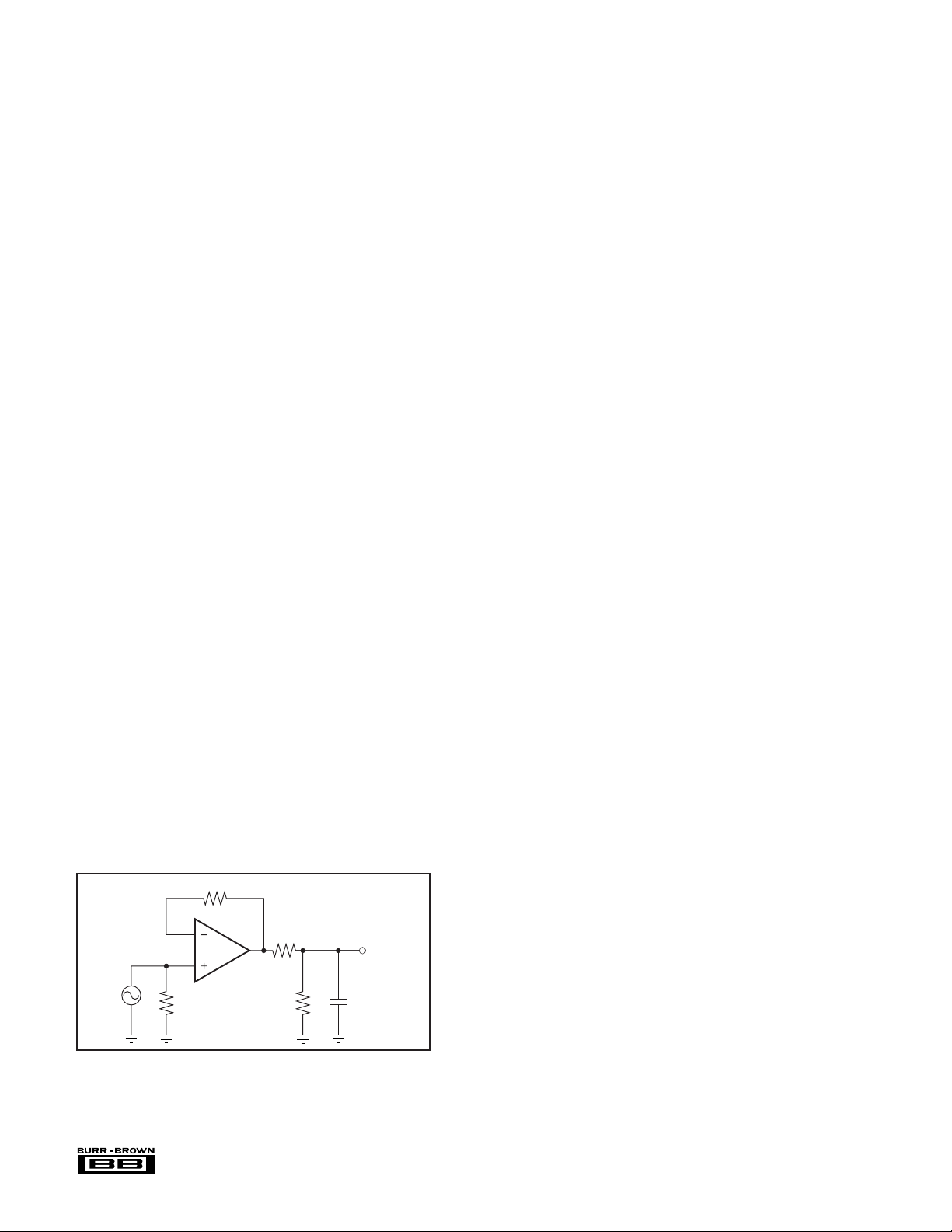
DRIVING CAPACITIVE LOADS
The OPA4650’s output stage has been optimized to drive
low resistive loads. Capacitive loads will decrease phase
margin which may result in high frequency oscillations or
peaking. Capacitive loads greater than 10pF should be isolated by connecting a small resistance (15Ω to 30Ω) in series
with the output as shown in Figure 4. This is especially
important when driving the capacitive input of high-speed
A/D converters. Increasing the gain from +1 will improve
the capacitive load drive due to increased phase margin.
In general, capacitive loads should be minimized for optimum high frequency performance. Coax lines can be driven
if the cable is properly terminated. The capacitance of coax
cable (29pF/ft for RG-58) will not load the amplifier when
the cable is source and load terminated in its characteristic
impedance.
25Ω
OPA4650
(R
typically 5Ω to 20Ω)
ISO
R
ISO
R
L
C
L
FREQUENCY RESPONSE COMPENSATION
Each channel of the OPA4650 is internally compensated to
be stable at unity gain with a nominal 60° phase margin.
This lends itself well to wideband integrator and buffer
applications. Phase margin and frequency response flatness
will improve at higher gains. Recall that an inverting gain of
–1 is equivalent to a gain of +2 for bandwidth purposes, i.e.,
noise gain = 2. The external compensation techniques developed for voltage feedback op amps can be applied to this
)
device. For example, in the non-inverting configuration,
placing a capacitor across the feedback resistor will reduce
the gain to +1 starting at f = (1/2πR
). Alternatively, in the
FCF
inverting configuration, the bandwidth may be limited without modifying the inverting gain by placing a series RC
network to ground on the inverting node. This has the effect
of increasing the noise gain at high frequencies, thereby
2
limiting the bandwidth for the inverting input signal through
/
the gain-bandwidth product.
At higher gains, the gain-bandwidth of this voltage feedback
topology will limit bandwidth according to the open-loop
frequency response curve. For applications requiring a wider
bandwidth at higher gains, consider the quad current feedback model, OPA4658. In applications where a large feedback resistor is required (such as photodiode transimpedance
circuits), precautions must be taken to avoid gain peaking
due to the pole formed by the feedback resistor and the
summing junction capacitance. This pole can be compensated by connecting a small capacitor in parallel with the
feedback resistor, creating a cancelling zero term. In other
high-gain applications, use of a three-resistor “T” connection will reduce the feedback network impedance which
reacts with the parasitic capacitance at the summing node.
PULSE SETTLING TIME
High speed amplifiers like the OPA4650 are capable of
extremely fast settling time with a pulse input. Excellent
frequency response flatness and phase linearity are required
to get the best settling times. As shown in the specifications
table, settling time for a ±1V step at a gain of +1 for the
OPA4650 is extremely fast. The specification is defined as
the time required, after the input transition, for the output to
settle within a specified error band around its final value. For
a 2V step, 1% settling corresponds to an error band of
±20mV, 0.1% to an error band of ±2mV, and 0.01% to an
error band of ±0.2mV. For the best settling times, particularly into an ADC capacitive load, little or no peaking in the
frequency response can be allowed. Using the recommended
for capacitive loads will limit this peaking and reduce
R
ISO
the settling times. Fast, extremely fine scale settling (0.01%)
requires close attention to ground return currents in the
supply decoupling capacitors. For highest performance, consider the OPA642 which isolates the output stage decoupling
from the rest of the amplifier.
FIGURE 4. Driving Capacitive Loads.
®
OPA4650
10
Page 11
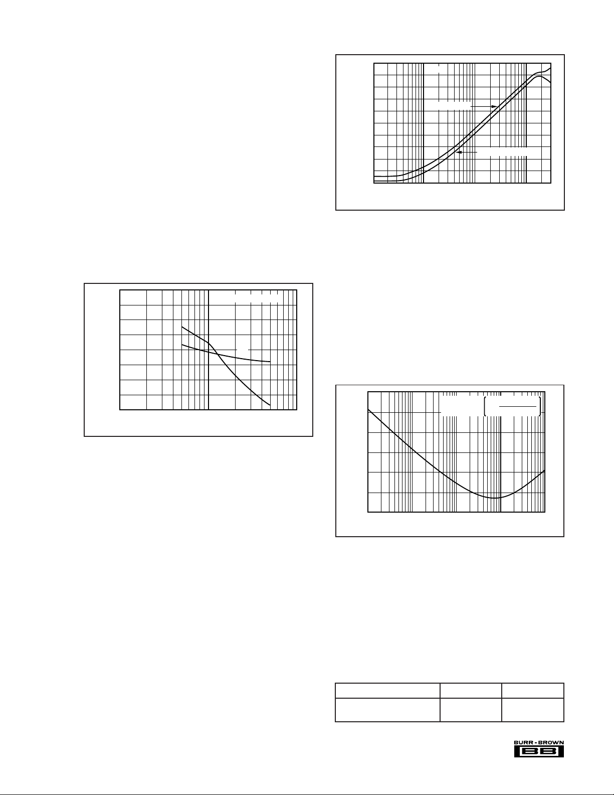
DIFFERENTIAL GAIN AND PHASE
0.1 1 10 100 300
Frequency (Hz)
–30
–40
–50
–60
–70
–80
Crosstalk (dB)
G = +1
All Hostile
Channel-to-Channel
Differential Gain (DG) and Differential Phase (DP) are
among the more important specifications for video applications. The percentage change in closed-loop gain over a
specified change in output voltage level is defined as DG.
DP is defined as the change in degrees of the closed-loop
phase over the same output voltage change. For the OPA4650,
DG and DP are both specified at the NTSC color sub-carrier
frequency of 3.58MHz and measured using industry standard video test equipment.
DISTORTION
The OPA4650’s harmonic distortion characteristics for a
100Ω load are shown in the Typical Performance Curves.
Distortion can be improved by increasing the load resistance
as illustrated in Figure 5. Remember to include the contribution of the feedback network when calculating the effective
load resistance seen by the amplifier.
–50
–60
–70
–80
Harmonic Distortion (dBc)
–90
10 100 1k
Load Resistance (Ω)
(fO = 5MHz, 2Vp-p)
2f
O
3f
O
FIGURE 5. Harmonic Distortion vs Load Resistance.
FIGURE 6. Channel-to-Channel Isolation and All Hostile
Crosstalk.
NOISE FIGURE
The voltage and current noise spectral density are shown in
the Typical Performance Curves. For RF and IF applications, however, Noise Figure (NF) is often the preferred
specification. This specification shows a degradation in
SNR through a device relative to the thermal noise of the
source impedance alone.
The NF for the OPA4650, using 1MHz spot noise numbers
and an unterminated non-inverting input, is shown in
Figure 7.
30
25
20
15
NF = 10 LOG 1 +
2
e
n
+ (InRS)
4KTR
2
S
CROSSTALK
Crosstalk is the undesired coupling of one channel’s signal
into the output of the other channels. Crosstalk is a consideration in all multichannel integrated circuits. The effect of
crosstalk is measured by driving one (“channel-to-channel”)
or more (“all-hostile”) channels and observing the output of
the undriven channel. The magnitude of this effect is expressed in the crosstalk specification as decibels of gain.
“Input referred” points to the fact that there is a direct
correlation between gain and crosstalk, therefore output
crosstalk increases proportionally at higher gains.
In quad devices, the effect of all-hostile crosstalk is observed
by driving all three channels concurrently and measuring the
output of the undriven fourth channel. The plots in Figure 6
illustrate both channel-to-channel and all-hostile crosstalk
for the OPA4650.
10
Noise Figure (dB)
5
0
10 100 1k 100k10k
Source Resistance (Ω)
FIGURE 7. Noise Figure vs Source Resistance.
SPICE MODELS AND EVALUATION BOARD
Computer simulation using SPICE is often useful when
analyzing the performance of analog circuits and systems.
This is particularly true for Video and RF amplifier circuits
where parasitic capacitance and inductance can have a
major effect on circuit performance. SPICE models and
evaluation PC boards are available for the OPA4650. Contact the Burr-Brown Applications Department to receive a
SPICE diskette.
DEMONSTRATION BOARD PACKAGE PRODUCT
DEM-OPA465xP 8-Pin DIP OPA4650P
DEM-OPA465xU SO-8 oPA4650U
11
OPA4650
®
Page 12
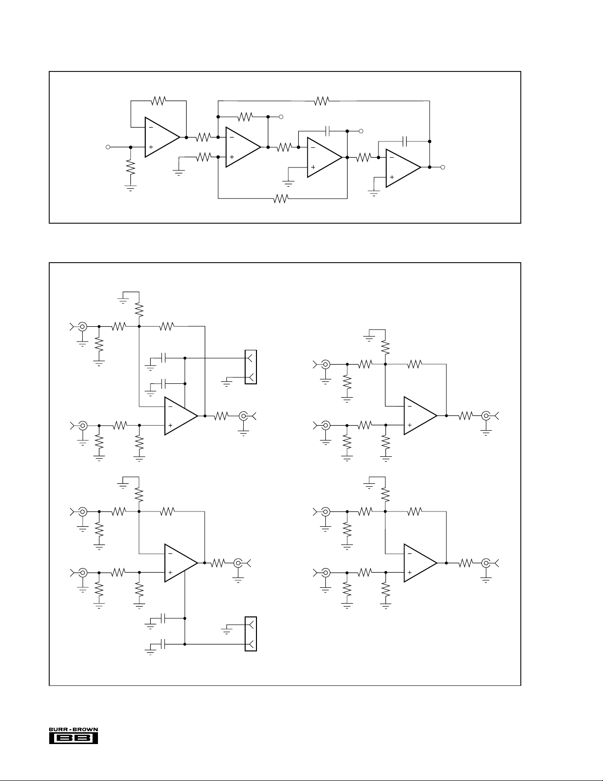
TYPICAL APPLICATION
25Ω
1/4
V
IN
FIGURE 8. State-Variable Biquadratic Filter.
–In
J
8
C
R
OPA4650
R
IN
R
32
17
R
18
1/4
OPA4650
High Pass
Output
1/4
OPA4650
Band Pass
Output
OPA4650
1/4
Low Pass
Output
+In
–In
+In
R
16
J
9
C
J
11
D
J
10
D
R
20
R
19
R
26
R
25
R
23
R
22
C
2
2.2µF
C
1
0.1µF
9
10
R
21
R
31
1/4
OPA4650
R
27
4
8
13
1/4
14
OPA4650
12
R
24
C
0.1µF
C
2.2µF
11
3
4
1
+5V
2
GND
–In
J
5
B
P1
J
R
7
15
R
28
Out
C
J
12
Out
D
1
GND
2
–5V
+In
–In
+In
J
4
B
J
2
A
J
3
A
R
R
11
R
R
8
R
R
5
R
R
5
R
30
R
10
R
29
R
7
R
6
OPA4650
5
2
OPA4650
3
13
J
R
6
1/4
R
4
1/4
14
7
R
1
1
Out
B
J
1
Out
A
12
9
3
6
P2
FIGURE 9. Circuit Detail for the DEM-OPA465xP Board.
®
OPA4650
12
Page 13
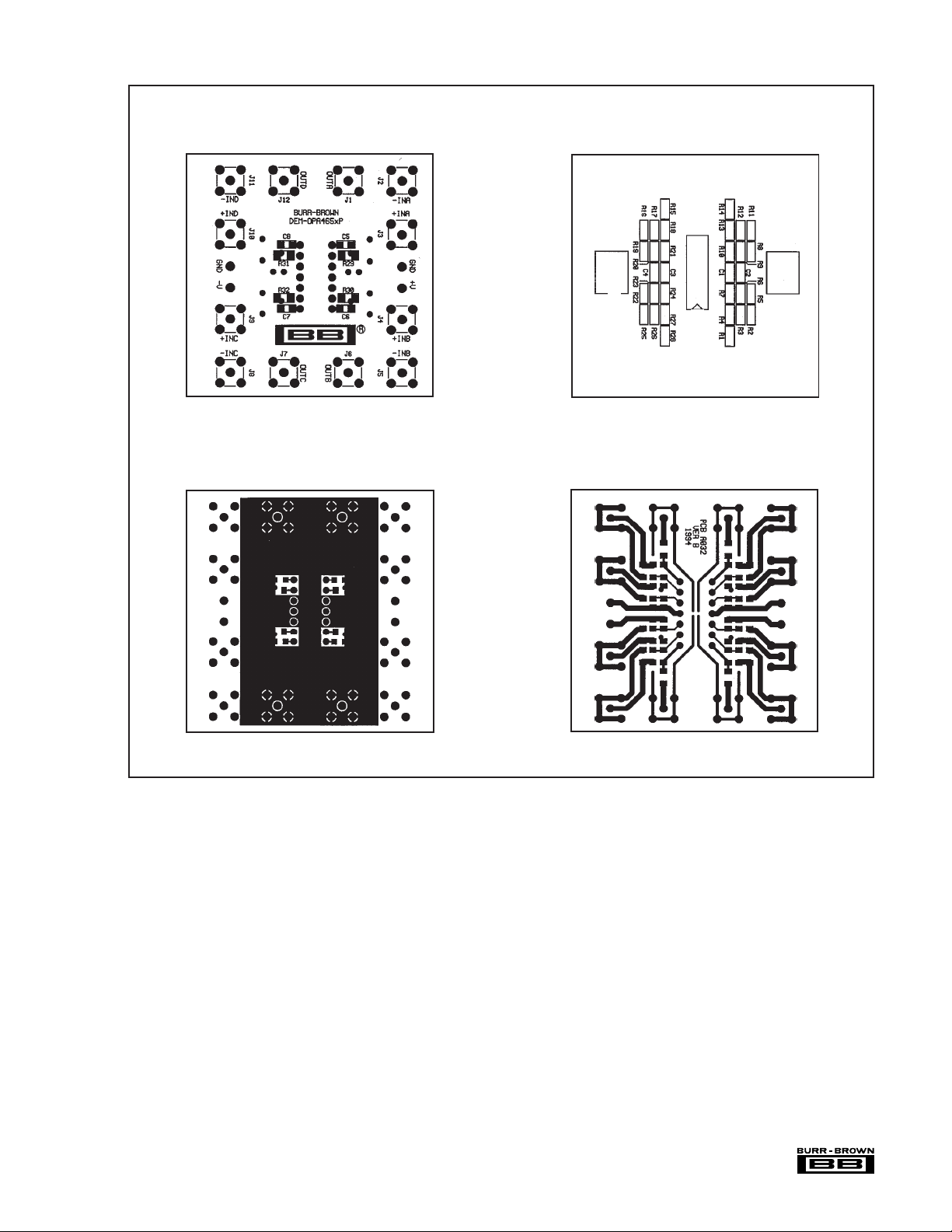
DEM-OPA465xP Demonstration Board Layout
(A)
P2
U1
P1
(B)
(C)
(D)
FIGURE 10a. Board Silkscreen (Bottom). 10b. Board Silkscreen (Top). 10c. Board Layout (Solder Side). 10d. Board Layout
(Component Side).
The information provided herein is believed to be reliable; however, BURR-BROWN assumes no responsibility for inaccuracies or omissions. BURR-BROWN assumes
no responsibility for the use of this information, and all use of such information shall be entirely at the user’s own risk. Prices and specifications are subject to change
without notice. No patent rights or licenses to any of the circuits described herein are implied or granted to any third party. BURR-BROWN does not authorize or warrant
any BURR-BROWN product for use in life support devices and/or systems.
13
OPA4650
®
 Loading...