

Burr Brown OPA445AU, OPA445AU-2K5, OPA445BM, OPA445AP Datasheet
1
2
3
4
5
6
7
8
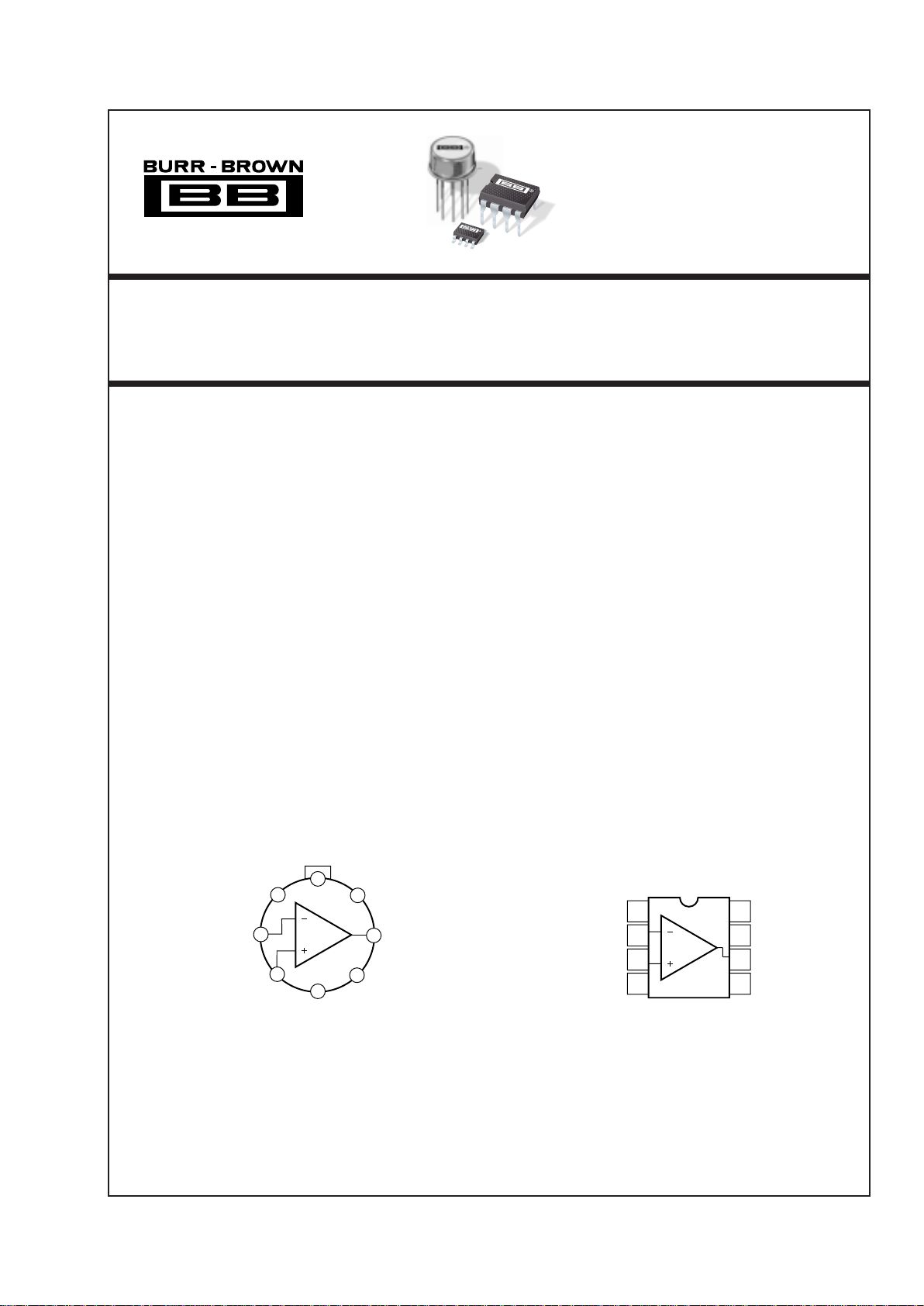
Offset Trim
V+
–In
+In
V–
Output
Offset Trim
NC
8-Pin DIP, SO-8
8
1
2
7
6
5
3
4
Offset
Trim
Offset
Trim
Output
V+
NC
–In
+In
V–
Case is connected to V–
TO-99
High Voltage FET-Input
OPERATIONAL AMPLIFIER
OPA445
®
FEATURES
● WIDE-POWER SUPPLY RANGE:
±10V to ±45V
● HIGH SLEW RATE: 15V/µs
● LOW INPUT BIAS CURRENT: 10pA
● STANDARD-PINOUT TO-99, DIP, AND
SURFACE-MOUNT PACKAGES
DESCRIPTION
The OPA445 is a monolithic operational amplifier
capable of operation from power supplies up to ±45V
and output currents of 15mA. It is useful in a wide
variety of applications requiring high output voltage
or large common-mode voltage swings.
The OPA445’s high slew rate provides wide powerbandwidth response, which is often required for highvoltage applications. FET input circuitry allows the
use of high-impedance feedback networks, thus mini-
mizing their output loading effects. Laser trimming of
the input circuitry yields low input offset voltage and
drift.
The OPA445 is available in standard pin-out TO-99,
DIP-8, and SO-8 surface-mount packages. It is fully
specified from –25°C to +85°C and operates from
–55°C to +125°C. A SPICE macromodel is available
for design analysis.
APPLICATIONS
● TEST EQUIPMENT
● HIGH-VOLTAGE REGULATORS
● POWER AMPLIFIERS
● DATA ACQUISITION
● SIGNAL CONDITIONING
● AUDIO
● PIEZO DRIVERS
©
1987 Burr-Brown Corporation PDS-754H Printed in U.S.A. March, 2000
OPA445
OPA445
For most current data sheet and other product
information, visit www.burr-brown.com
International Airport Industrial Park • Mailing Address: PO Box 11400, Tucson, AZ 85734 • Street Address: 6730 S. Tucson Blvd., Tucson, AZ 85706 • Tel: (520) 746-1111
Twx: 910-952-1111 • Internet: http://www.burr-brown.com/ • Cable: BBRCORP • Telex: 066-6491 • FAX: (520) 889-1510 • Immediate Product Info: (800) 548-6132

2
®
OPA445
SPECIFICATIONS
At TA = +25°C, VS = ±40V, and RL = 5kΩ, unless otherwise specified.
Boldface limits apply over the specified temperature range, T
A
= –25°C to +85°C. VS = ±40V.
The information provided herein is believed to be reliable; however, BURR-BROWN assumes no responsibility for inaccuracies or omissions. BURR-BROWN assumes
no responsibility for the use of this information, and all use of such information shall be entirely at the user’s own risk. Prices and specifications are subject to change
without notice. No patent rights or licenses to any of the circuits described herein are implied or granted to any third party. BURR-BROWN does not authorize or warrant
any BURR-BROWN product for use in life support devices and/or systems.
OPA445BM OPA445AP, AU
PARAMETER CONDITIONS MIN TYP MAX MIN TYP MAX UNITS
OFFSET VOLTAGE
Input Offset Voltage V
OS
VCM = 0, IO = 0 ±1 ±3 ±1.5 ±5mV
vs Temperature V
OS
/dT TA = –25°C to +85°C ±10 ✻ µV/°C
vs Power Supply PSRR V
S
= ±10V to ±45V 4 100 ✻✻µV/V
INPUT BIAS CURRENT
(1)
Input Bias Current I
B
VCM = 0V ±10 ±50 ✻ ±100 pA
Over Specified Temperature Range
±10 ±20 nA
Input Offset Current I
OS
VCM = 0V ±4 ±20 ✻ ±40 pA
Over Specified Temperature Range
±5 ±10 nA
NOISE
Input Voltage Noise Density, f = 1kHz
e
n
15 ✻ nV/√Hz
Current Noise Density, f = 1kHz i
n
6 ✻ fA/√Hz
INPUT VOLTAGE RANGE
Common-Mode Voltage Range V
CM
VS = ±40V (V–)+5 (V+)–5 ✻✻V
Common-Mode Rejection CMRR V
CM
= –35V to +35V 80 95 ✻✻ dB
Over Specified Temperature Range
80 ✻ dB
INPUT IMPEDANCE
Differential 10
13
|| 1 ✻ Ω || pF
Common-Mode 10
14
|| 3 ✻ Ω || pF
OPEN-LOOP GAIN, DC
Open-Loop Voltage Gain A
OL
VO = –35V to +35V 100 110 ✻✻ dB
Over Specified Temperature Range
97 ✻ dB
FREQUENCY RESPONSE
Gain Bandwidth Product GBW 2 ✻ MHz
Slew Rate SR V
O
= 70Vp-p 5 15 ✻✻ V/µs
Full Power Bandwidth V
O
= 70Vp-p 23 70 ✻✻ kHz
Rise Time V
O
= ±200mV 100 ✻ ns
Overshoot G = +1, Z
L
= 5kΩ || 50pF 35 ✻ %
Total Harmonic Distortion + Noise
THD+N
f = 1kHz, VO = 3.5Vr ms, G = 1 0.0002 ✻ %
f = 1kHz, V
O
= 10Vr ms, G = 1 0.00008 ✻ %
OUTPUT
Voltage Output V
O
(V–)+5 (V+)–5 ✻✻V
Over Specified Temperature Range
(V–)+5 (V+)–5 ✻✻V
Current Output I
O
VO = ±28V ±15 ✻ mA
Output Resistance, Open Loop R
O
dc 220 ✻ Ω
Short Circuit Current I
SC
±26 ✻ mA
Capacitive Load Drive C
LOAD
See Typical Curve
(2)
✻
POWER SUPPLY
Specified Operating Range V
S
±40 ✻ V
Operating Voltage Range ±10 ±45 ✻✻V
Quiescent Current I
Q
IO = 0 ±4.2 ±4.7 ✻✻mA
TEMPERATURE RANGE
Specification Range –25 +85 ✻✻°C
Operating Range –55 +125 ✻✻°C
Storage Range –65 +125 –55 +125 °C
Thermal Resistance
θ
JA
TO-99 200 °C/W
8-Pin DIP 100 °C/W
SO-8 Surface-Mount 150 °C/W
✻ Specifications same as OPA445BM.
NOTE: (1) High-speed test at T
J
= +25°C. (2) See “Small-Signal Overshoot vs Load Capacitance” in the Typical Performance Curves section.

3
®
OPA445
ABSOLUTE MAXIMUM RATINGS
(1)
Power Supply..................................................................................... ±50V
Differential Input Voltage ................................................................... ±80V
Input Voltage Range ...................................................................|±V
S
| –3V
Storage Temperature Range: M ..................................... –65°C to +150°C
P, U................................. –55°C to +125°C
Operating Temperature Range ....................................... –55°C to +125°C
Lead Temperature (soldering, 10s) ............................................... +300°C
Output Short-Circuit to Ground (T
J
< +125°C) ......................... Continuous
Junction Temperature: M ................................................................. 175°C
P,U.............................................................. 150°C
NOTE: (1) Stresses above these ratings may cause permanent damage.
Exposure to absolute maximum conditions for extended periods may degrade
device reliability.
ELECTROSTATIC
DISCHARGE SENSITIVITY
This integrated circuit can be damaged by ESD. Burr-Brown
recommends that all integrated circuits be handled with
appropriate precautions. Failure to observe proper handling
and installation procedures can cause damage.
ESD damage can range from subtle performance degradation
to complete device failure. Precision integrated circuits may
be more susceptible to damage because very small parametric
changes could cause the device not to meet its published
specifications.
PACKAGE/ORDERING INFORMATION
PACKAGE SPECIFIED
DRAWING TEMPERATURE PACKAGE ORDERING TRANSPORT
PRODUCT PACKAGE NUMBER RANGE MARKING NUMBER
(1)
MEDIA
OPA445AP 8-Pin DIP 006 –25°C to +85°C OPA445AP OPA445AP Rails
OPA445AU SO-8 Surface-Mount 182 –25°C to +85°C OPA445AU OPA445AU Rails
OPA445AU " " " " OPA445AU/2K5 Tape and Reel
OPA445BM 8-Pin TO-99 001 –25°C to +85°C OPA445BM OPA445BM Rails
NOTE: (1) Products followed by a slash (/) are only available in Tape and Reel in the quantities indicated (e.g., /2K5 indicates 2500 devices per reel). Ordering 2500
pieces of “OPA445AU/2K5” will get a single 2500 piece Tape and Reel.
4
®
OPA445
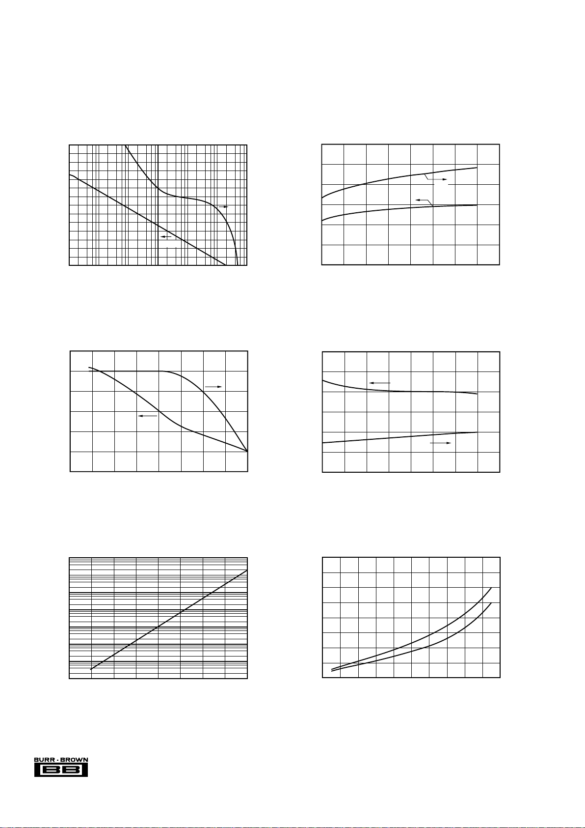
TYPICAL PERFORMANCE CURVES
At TA = +25°C, VS = ±40V, unless otherwise noted.
–75 0–50 –25 25 75 100 125
Temperature (°C)
0.01pA
100nA
10nA
1nA
100pA
10pA
1pA
0.1pA
Input Bias Current
INPUT BIAS CURRENT
vs TEMPERATURE
50
10 1k100 10k 1M 10M
Frequency (Hz)
0
140
120
100
80
60
40
20
Voltage Gain (dB)
OPEN-LOOP GAIN AND PHASE
vs FREQUENCY
100k
Gain
θ
–185
–45
–90
–135
Phase (Degrees)
GBW
–75 0–50 –25 25 75 100 125
Ambient Temperature (°C)
1.4
2.6
2.4
2.2
2.0
1.8
1.6
Gain Bandwidth (MHz)
GAIN BANDWIDTH AND SLEW RATE
vs TEMPERATURE
SR
10
16
15
14
13
12
11
50
Slew Rate (V/µs)
GBW
10 20 30 40 50
Supply Voltage (±V
S
)
1.6
2.2
2.0
1.8
Gain Bandwidth (MHz)
GAIN BANDWIDTH AND SLEW RATE
vs SUPPLY VOLTAGE
Slew Rate (V/µs)
SR
13
19
17
15
10 20 30 40 50
Supply Voltage (±V
S
)
125
120
115
110
105
100
95
Voltage Gain (dB)
OPEN-LOOP GAIN AND SUPPLY CURRENT
vs SUPPLY VOLTAGE
Supply Current (mA)
A
VOL
3.0
4.5
4.0
3.5
I
Q
–50 –40 –30 –20 –10
–I
B
+I
B
0 1020304050
Common-Mode Voltage (V)
40
35
30
25
20
15
10
5
0
Bias Current (pA)
INPUT BIAS CURRENT
vs COMMON-MODE VOLTAGE
 Loading...