

Burr Brown OPA2353EA-250, OPA2353EA-2K5, OPA2353UA-2K5, OPA2353UA, OPA353UA Datasheet
...
®
O
OPA2353
P
A4353
OPA4353
OPA353
OPA2353
For most current data sheet and other product
information, visit www.burr-brown.com
High-Speed, Single-Supply, Rail-to-Rail
OPERA TIONAL AMPLIFIERS
Micro
FEATURES
● RAIL-TO-RAIL INPUT
● RAIL-TO-RAIL OUTPUT (within 10mV)
● WIDE BANDWIDTH: 44MHz
● HIGH SLEW RATE: 22V/µs
● LOW NOISE: 5nV/√Hz
● LOW THD+NOISE: 0.0006%
● UNITY-GAIN STABLE
●
Micro
SIZE PACKAGES
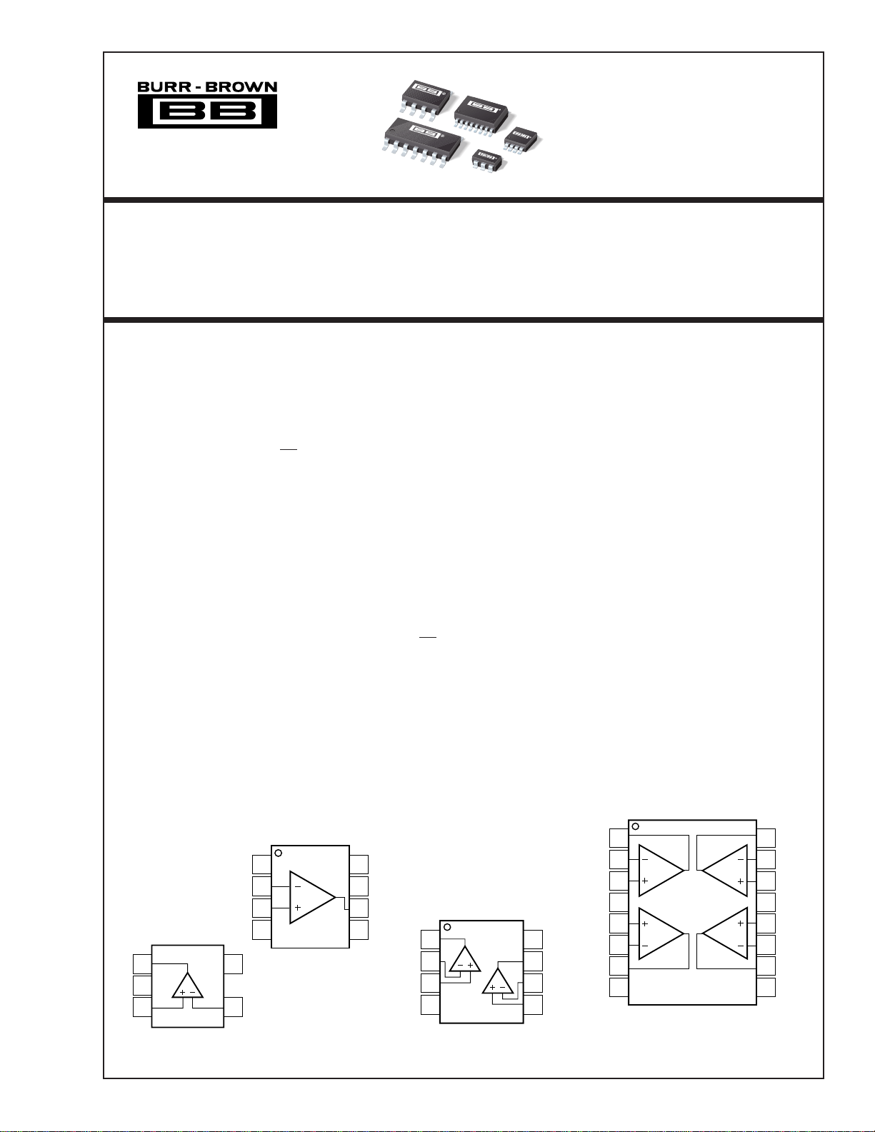
● SINGLE, DUAL, AND QUAD
DESCRIPTION
OPA353 series rail-to-rail CMOS operational amplifiers are designed for low cost, miniature applications.
They are optimized for low voltage, single-supply operation. Rail-to-rail input/output, low noise (5nV/√Hz),
and high speed operation (44MHz, 22V/µs) make them
ideal for driving sampling analog-to-digital converters.
They are also well suited for cell phone PA control
loops and video processing (75Ω drive capability) as
well as audio and general purpose applications. Single,
dual, and quad versions have identical specifications
for design flexibility.
The OPA353 series operates on a single supply as low as
2.5V with an input common-mode voltage range that
SPICE Model available at www.burr-brown.com
Amplifier
OPA4353
™
Series
APPLICATIONS
● CELL PHONE PA CONTROL LOOPS
● DRIVING A/D CONVERTERS
● VIDEO PROCESSING
● DATA ACQUISITION
● PROCESS CONTROL
● AUDIO PROCESSING
● COMMUNICATIONS
● ACTIVE FILTERS
● TEST EQUIPMENT
extends 300mV beyond the supply rails. Output voltage
swing is to within 10mV of the supply rails with a 10kΩ
load. Dual and quad designs feature completely independent circuitry for lowest crosstalk and freedom from
interaction.
The single (OPA353) packages are the tiny 5-lead SOT23-5 surface mount and SO-8 surface mount. The dual
(OPA2353) comes in the miniature MSOP-8 surface
mount and SO-8 surface mount. The quad (OPA4353)
packages are the space-saving SSOP-16 surface mount
and SO-14 surface mount. All are specified from –40°C
to +85°C and operate from –55°C to +125°C.
OPA4353
OPA353
NC
1
–In
2
+In
3
V–
OPA353
Out
1
V–
2
+In
3
SOT-23-5
International Airport Industrial Park • Mailing Address: PO Box 11400, Tucson, AZ 85734 • Street Address: 6730 S. Tucson Blvd., Tucson, AZ 85706 • Tel: (520) 746-1111
Twx: 910-952-1111 • Internet: http://www.burr-brown.com/ • Cable: BBRCORP • Telex: 066-6491 • FAX: (520) 889-1510 • Immediate Product Info: (800) 548-6132
© 1998 Burr-Brown Corporation PDS-1479B Printed in U.S.A. March, 1999
4
V+
5
–In
4
SO-8
NC
8
V+
7
Output
6
NC
5
Out A
–In A
+In A
V–
1
2
3
4
SO-8, MSOP-8
OPA2353
A
8
7
B
6
5
V+
Out B
–In B
+In B
Out A
–In A
+In A
+V
+In B
–In B
Out B
NC
1
2
AD
3
4
5
BC
6
7
8
SSOP-16
(SO-14 package not shown)
Out D
16
–In D
15
+In D
14
–V
13
+In C
12
–In C
11
Out C
10
NC
9
SPECIFICATIONS: VS = 2.7V to 5.5V
At TA = +25°C, RL = 1kΩ connected to VS/ 2 and V
Boldface limits apply over the specified temperature range, T
PARAMETER CONDITION MIN TYP
OFFSET VOLTAGE
Input Offset Voltage V
= –40°C to +85°C ±10 mV
T
A
vs Temperature T
vs Power Supply Rejection Ratio PSRR V
= –40°C to +85°C VS = 2.7V to 5.5V, VCM = 0V 175 µV/V
T
A
Channel Separation (dual, quad) dc 0.15 µV/V
INPUT BIAS CURRENT
Input Bias Current I
T
= –40°C to +85°C See Typical Curve
A
Input Offset Current I
NOISE
Input Voltage Noise, f = 100Hz to 400kHz 4 µVrms
Input Voltage Noise Density, f = 10kHz e
f = 100kHz 5 nV/√Hz
Current Noise Density, f = 10kHz i
INPUT VOLTAGE RANGE
Common-Mode Voltage Range V
Common-Mode Rejection Ratio CMRR –0.1V < V
= –40°C to +85°C VS = 5V, –0.1V < V
T
A
INPUT IMPEDANCE
Differential 10
Common-Mode 10
OPEN-LOOP GAIN
Open-Loop Voltage Gain A
= –40°C to +85°C RL = 10kΩ, 50mV < VO < (V+) – 50mV 100 dB
T
A
= –40°C to +85°C RL = 1kΩ, 200mV < VO < (V+) – 200mV 100 dB
T
A
FREQUENCY RESPONSE C
Gain-Bandwidth Product GBW G = 1 44 MHz
Slew Rate SR G = 1 22 V/ µs
Settling Time, 0.1% G = ±1, 2V Step 0.22 µs
0.01% G = ±1, 2V Step 0.5 µs
Overload Recovery Time V
Total Harmonic Distortion + Noise THD+N
Differential Gain Error G = 2, R
Differential Phase Error G = 2, R
OUTPUT
Voltage Output Swing from Rail
= –40°C to +85°C RL = 10kΩ, AOL ≥ 100dB 50 mV
T
A
= –40°C to +85°C RL = 1kΩ, A
T
A
Output Current I
Short-Circuit Current I
Capacitive Load Drive C
(4)
V
LOAD
OUT
OUT
POWER SUPPLY
Operating Voltage Range V
Minimum Operating Voltage 2.5 V
Quiescent Current (per amplifier) I
= –40°C to +85°C IO = 0 9 mA
T
A
TEMPERATURE RANGE
Specified Range –40 +85 °C
Operating Range –55 +125 °C
Storage Range –55 +125 °C
Thermal Resistance
SOT-23-5 200 °C/W
MSOP-8 Surface Mount 150 °C/W
SO-8 Surface Mount 150 °C/W
SSOP-16 Surface Mount 100 °C/W
SO-14 Surface Mount 100 °C/W
NOTES: (1) V
the output and power supply rails. (5) See typical performance curve, “Output Voltage Swing vs Output Swing.”
= +5V. (2) V
S
= 0.25V to 2.75V. (3) NTSC signal generator used. See Figure 6 for test circuit. (4) Output voltage swings are measured between
OUT
= VS/ 2, unless otherwise noted.
OUT
= –40°C to +85°C. VS = 5V.
A
OPA353NA, UA
OPA2353EA, UA
OPA4353EA, UA
(1)
OS
B
OS
n
n
CM
V
RL = 10kΩ, 50mV < VO < (V+) – 50mV 100 122 dB
OL
= 1kΩ, 200mV < VO < (V+) – 200mV 100 120 dB
R
L
RL = 600Ω, VO = 2.5Vp-p
VS = 5V ±3 ±8mV
= –40°C to +85°C ±5 µV/°C
A
= 2.7V to 5.5V, VCM = 0V 40 150 µV/V
S
±0.5 ±10 pA
±0.5 ±10 pA
7 nV/√Hz
4 fA/√Hz
–0.1 (V+) + 0.1 V
< (V+) – 2.4V 76 86 dB
CM
= 5V, –0.1V < V
S
= 100pF
L
• G = V
IN
= 600Ω, VO = 1.4V
L
= 600Ω, VO = 1.4V
L
< 5.1V 60 74 dB
CM
< 5.1V 58 dB
CM
13
|| 2.5 Ω || pF
13
|| 6.5 Ω || pF
S
(2)
, G = 1, f = 1kHz
(3)
(3)
0.1 µs
0.0006 %
0.17 %
0.17 deg
MAX UNITS
RL = 10kΩ, AOL ≥ 100dB 10 50 mV
= 1kΩ, AOL ≥ 100dB 25 200 mV
R
L
SC
S
Q
θ
JA
TA = –40°C to +85°C 2.7 5.5 V
≥ 100dB 200 mV
OL
±40
(5)
±80 mA
See Typical Curve
IO = 0 5.2 8 mA
mA
®
OPA353, 2353, 4353
2
PIN CONFIGURATION
Top View SO-14
OPA4353
Out A
–In A
+In A
V+
+In B
–In B
Out B
1
2
3
4
5
6
7
AD
BC
Out D
14
–In D
13
+In D
12
V–
11
+In C
10
–In C
9
Out C
8
ELECTROSTATIC
DISCHARGE SENSITIVITY
This integrated circuit can be damaged by ESD. Burr-Brown
recommends that all integrated circuits be handled with
appropriate precautions. Failure to observe proper handling
and installation procedures can cause damage.
ESD damage can range from subtle performance degradation to complete device failure. Precision integrated circuits
may be more susceptible to damage because very small
parametric changes could cause the device not to meet its
published specifications.
ABSOLUTE MAXIMUM RATINGS
Supply Voltage ................................................................................... 5.5V
Signal Input Terminals, Voltage
Output Short-Circuit
Operating Temperature ..................................................–55 °C to +125°C
Storage Temperature ..................................................... –55°C to +125°C
Junction Temperature ...................................................................... 150°C
Lead Temperature (soldering, 10s) ................................................. 300°C
NOTES: (1) Stresses above these ratings may cause permanent damage.
Exposure to absolute maximum conditions for extended periods may degrade device reliability. (2) Input terminals are diode-clamped to the power
supply rails. Input signals that can swing more than 0.3V beyond the supply
rails should be current-limited to 10mA or less. (3) Short circuit to ground,
one amplifier per package.
(3)
(2)
.................. (V–) – 0.3V to (V+) + 0.3V
(2)
Current
.............................................................. Continuous
.................................................... 10mA
(1)
PACKAGE/ORDERING INFORMATION
PACKAGE SPECIFIED
PRODUCT PACKAGE NUMBER
DRAWING TEMPERATURE PACKAGE ORDERING TRANSPORT
Single
OPA353NA 5-Lead SOT-23-5 331 –40°C to +85°C D53 OPA353NA/250 Tape and Reel
"""""OPA353NA /3K Tape and Reel
OPA353UA SO-8 Surface Mount 182 –40°C to +85°C OPA353UA OPA353UA Rails
"""""OPA353UA /2K5 Tape and Reel
Dual
OPA2353EA MSOP-8 Surface Mount 337 –40°C to +85°C E53 OPA2353EA /250 Tape and Reel
"""""OPA2353EA/2K5 Tape and Reel
OPA2353UA SO-8 Surface Mount 182 –40 °C to +85°C OPA2353UA OPA2353UA Rails
"""""OPA2353UA/2K5 Tape and Reel
Quad
OPA4353EA SSOP-16 Surface Mount 322 –40°C to +85°C OPA4353EA OPA4353EA /250 Tape and Reel
"""""OPA4353EA /2K5 Tape and Reel
OPA4353UA SO-14 Surface Mount 235 –40°C to +85°C OPA4353UA OPA4353UA Rails
"""""OPA4353UA/2K5 Tape and Reel
NOTES: (1) For detailed drawing and dimension table, please see end of data sheet, or Appendix C of Burr-Brown IC Data Book. (2) Models with a slash (/) are
available only in Tape and Reel in the quantities indicated (e.g., /2K5 indicates 2500 devices per reel). Ordering 2500 pieces of “OPA2353EA/2K5” will get a single
2500-piece Tape and Reel. For detailed Tape and Reel mechanical information, refer to Appendix B of Burr-Brown IC Data Book.
(1)
RANGE MARKING NUMBER
(2)
MEDIA
The information provided herein is believed to be reliable; however, BURR-BROWN assumes no responsibility for inaccuracies or omissions. BURR-BROWN assumes no responsibility
for the use of this information, and all use of such information shall be entirely at the user’s own risk. Prices and specifications are subject to change without notice. No patent rights or
licenses to any of the circuits described herein are implied or granted to any third party. BURR-BROWN does not authorize or warrant any BURR-BROWN product for use in life support
devices and/or systems.
®
3
OPA353, 2353, 4353
TYPICAL PERFORMANCE CURVES
At TA = +25°C, VS = +5V, and RL = 1kΩ connected to VS/2, unless otherwise noted.
160
140
120
100
80
60
Voltage Gain (dB)
40
20
0
0.1 1
100k
10k
1k
100
Voltage Noise (nV√Hz)
10
1
10 100 1k 10k 100k 1M 10M
OPEN-LOOP GAIN/PHASE vs FREQUENCY
G
10 100 1k 10k 100k 1M 10M 100M
Frequency (Hz)
INPUT VOLTAGE AND CURRENT NOISE
SPECTRAL DENSITY vs FREQUENCY
Current Noise
Voltage Noise
Frequency (Hz)
POWER SUPPLY AND COMMON-MODE
0
–45
φ
10k
1k
100
10
1
0.1
–90
–135
–180
Current Noise (fA√Hz)
100
90
80
70
60
50
Phase (°)
40
30
PSRR, CMRR (dB)
20
10
0
10 100 1k 10k 100k 1M 10M
140
130
120
110
100
90
80
Channel Separation (dB)
70
60
REJECTION RATIO vs FREQUENCY
PSRR
CMRR
(V
= +5V
S
V
= –0.1V to 5.1V)
CM
Frequency (Hz)
CHANNEL SEPARATION vs FREQUENCY
Dual and Quad
Versions
10010 1k 1M100k10k 10M
Frequency (Hz)
TOTAL HARMONIC DISTORTION + NOISE
1
G = 100, 3Vp-p (VO = 1V to 4V)
0.1
0.01
THD+N (%)
0.001
0.0001
G = 10, 3Vp-p (VO = 1V to 4V)
G = 1, 3Vp-p (VO = 1V to 4V)
Input goes through transition region
G = 1, 2.5Vp-p (VO = 0.25V to 2.75V)
Input does NOT go through transition region
10 100 1k 10k 100k
®
vs FREQUENCY
Frequency (Hz)
OPA353, 2353, 4353
RL = 600Ω
(–40dBc)
0.1
(–60dBc)
0.01
(–80dBc)
0.001
Harmonic Distortion (%)
(–100dBc)
0.0001
(–120dBc)
4
HARMONIC DISTORTION + NOISE vs FREQUENCY
1
G = 1
= 2.5Vp-p
V
O
= 600Ω
R
L
3rd Harmonic
1k 10k 100k 1M
2nd Harmonic
Frequency (Hz)
 Loading...