

Burr Brown OPA4243EA-2K5, OPA4243EA Datasheet
1
®
OPA4243
FEATURES
● MICRO-SIZE, TSSOP PACKAGE
● SINGLE-SUPPLY OPERATION
● WIDE SUPPLY RANGE: 2.2V to 36V
● LOW QUIESCENT CURRENT: 45µA/chan
● WIDE BANDWIDTH: 430kHz
● WIDE INPUT/OUTPUT SWING
DESCRIPTION
The OPA4243 is a four-channel op amp specifically
designed for high density, space-limited applications,
such as LCD bias drivers, PCMCIA cards, batterypacks and portable instruments. In addition to small
size, this part features wide output swing, very low
quiescent current, and low bias current. Other features
include unity gain stability and the best speed power
ratio available. Power supplies in the range of 2.2V to
36V (±1.1V to ±18V) can be used.
Each channel uses completely independent circuitry
for lowest crosstalk and freedom from interaction,
even when overloaded. In addition, the amplifier is
free from output inversion when the inputs are driven
to the rail. The OPA4243EA is supplied in the miniature TSSOP-14 surface mount package. Specifications
apply from –40°C to +85°C. However, as the extensive typical performance curves indicate, the OPA4243
can be used over the full –55°C to +125°C range. A
SPICE macromodel is available for design analysis.
Quad OPERATIONAL AMPLIFIER
Micro
POWER, Single-Supply
®
OPA4243
APPLICATIONS
● LCD DISPLAY DRIVERS
● BATTERY POWERED SYSTEMS
● PORTABLE EQUIPMENT
● PCMCIA CARDS
● BATTERY PACKS AND POWER SUPPLIES
● CONSUMER PRODUCTS
© 1999 Burr-Brown Corporation PDS-1562A Printed in U.S.A. November, 1999
For most current data sheet and other product
information, visit www.burr-brown.com
®
OPA4243
International Airport Industrial Park • Mailing Address: PO Box 11400, Tucson, AZ 85734 • Street Address: 6730 S. Tucson Blvd., Tucson, AZ 85706 • Tel: (520) 746-1111
Twx: 910-952-1111 • Internet: http://www.burr-brown.com/ • Cable: BBRCORP • Telex: 066-6491 • FAX: (520) 889-1510 • Immediate Product Info: (800) 548-6132
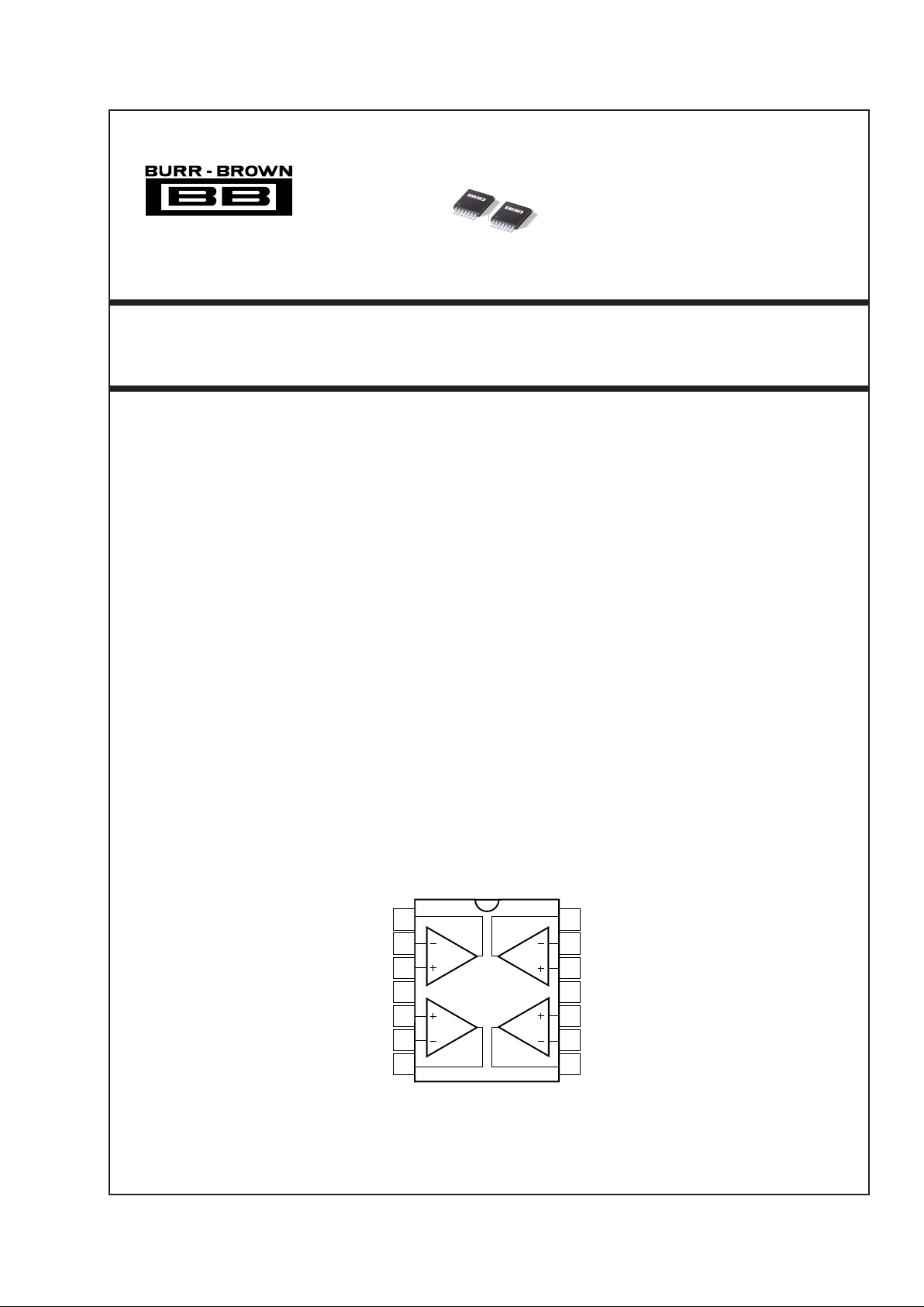
1
2
3
4
5
6
7
14
13
12
11
10
9
8
Output D
–Input D
+Input D
–V
+Input C
–Input C
Output C
Output A
–Input A
+Input A
+V
+Input B
–Input B
Output B
OPA4243EA
TSSOP-14
®
OPA4243

2
®
OPA4243
SPECIFICATIONS: VS = +2.6V to +36V
Boldface limits apply over the specified temperature range, TA = –40°C to +85°C
At TA = +25°C, RL = 20kΩ connected to ground, unless otherwise noted.
OPA4243EA
PARAMETER CONDITIONS MIN TYP
(1)
MAX UNITS
OFFSET VOLTAGE
Input Offset Voltage V
OS
VS = ±7.5V, V
CM
= 0 ±2 ±5mV
Over Temperature
±6 mV
vs Temperature dV
OS
/dT TA = –40°C to +85°C ±2.5 µV/°C
vs Power Supply PSRR V
S
= +2.6V to +36V 2.5 100 µV/V
Over Temperature V
S
= +2.6V to +36V 100 µV/V
Channel Separation 140 dB
INPUT BIAS CURRENT
Input Bias Current I
R
VCM = VS/2 –10 –25 nA
Input Offset Current I
OS
VCM = VS/2 ±1 ±10 nA
NOISE
Input Noise Voltage, f = 0.1 to 10Hz 0.4 µVp-p
Input Noise Voltage Density, f = 1kHz e
n
22 nV/√Hz
Current Noise Density, f = 1kHz i
n
40 fA/√Hz
INPUT VOLTAGE RANGE
Common-Mode Voltage Range V
CM
0 (V+) – 0.9 V
Common-Mode Rejection CMRR V
S
= ±18V, VCM = –18V to +17.1V 82 104 dB
Over Temperature V
S
= ±18V, VCM = –18V to +17.1V 82 dB
INPUT IMPEDANCE
Differential 10
6
|| 2 Ω || pF
Common-Mode 10
9
|| 2 Ω || pF
OPEN-LOOP GAIN
Open-Loop Voltage Gain A
OL
VO = 0.5V to (V+) – 0.9 86 104 dB
Over Temperature V
O
= 0.5V to (V+) – 0.9 86 dB
FREQUENCY RESPONSE
Gain-Bandwidth Product GBW 430 kHz
Slew Rate SR G = 1 –0.1, ±0.16 V/µs
Setting Time, 0.01% 10V Step 150 µs
Overload Recovery Time V
IN
• Gain = V
S
8 µs
OUTPUT
Voltage Output, Positive V
O
A
OL ≥
80dB, RL = 20kΩ to VS/2 (V+) – 0.9 (V+) – 0.75 V
Over Temperature A
OL ≥
80dB, RL = 20kΩ to VS/2 (V+) – 0.9 (V+) – 0.75 V
Voltage Output, Negative A
OL ≥
80dB, RL = 20kΩ to VS/2 0.5 0.2 V
Over Temperature A
OL ≥
80dB, RL = 20kΩ to VS/2 0.5 0.2 V
Voltage Output, Positive A
OL ≥
80dB, RL = 20kΩ to Ground (V+) – 0.75 V
Over Temperature A
OL ≥
80dB, RL = 20kΩ to Ground (V+) – 0.75 V
Voltage Output, Negative A
OL ≥
80dB, RL = 20kΩ to Ground 0.1 V
Over Temperature A
OL ≥
80dB, RL = 20kΩ to Ground 0.1 V
Short-Circuit Current I
SC
–25, +12 mA
Capacitive Load Drive C
LOAD
See Typical Curve
POWER SUPPLY
Specified Voltage Range V
S
Over Temperature +2.6 +36 V
Minimum Operating Voltage +2.2 V
Quiescent Current I
O
IO = 0 45 60 µA
Over Temperature I
O
= 0 70 µA
TEMPERATURE RANGE
Specified Range –40 85 °C
Operating Range –55 125 °C
Storage Range –65 150 °C
Thermal Resistance
θ
JA
TSSOP-14 Surface Mount 100 °C/W
NOTE: (1) V
S
= +15V.
3
®
OPA4243
Supply Voltage, V+ to V– .................................................................... 36V
Input Voltage Range
(2)
................................... (V–) – 0.3V to (V+) + 0.3V
Input Current
(2)
................................................................................. 10mA
Output Short-Circuit
(3)
.............................................................. Continuous
Operating Temperature .................................................. –55°C to +125°C
Storage Temperature ..................................................... –65°C to +150°C
Junction Temperature ...................................................................... 150°C
Lead Temperature (soldering, 10s) ................................................. 300°C
ESD Capability ................................................................................ 2000V
NOTES: (1) Stresses above these ratings may cause permanent damage.
Exposure to absolute maximum conditions for extended periods may degrade
device reliability. (2) Inputs are diode-clamped to the supply rails and should
be current-limited to 10mA or less if input voltages can exceed rails by more
than 0.3V. (3) Short-circuit to ground, one amplifier per package.
ABSOLUTE MAXIMUM RATINGS
(1)
PACKAGE/ORDERING INFORMATION
PACKAGE SPECIFIED
DRAWING TEMPERATURE PACKAGE ORDERING TRANSPORT
PRODUCT PACKAGE NUMBER RANGE MARKING NUMBER
(1)
MEDIA
OPA4243EA TSSOP-14 357 –40°C to +85°C OPA4243EA OPA4243EA/250 Tape and Reel
"""""OPA4243EA/2K5 Tape and Reel
NOTE: (1) Models with a slash (/) are available only in Tape and Reel in the quantities indicated (e.g., /2K5 indicates 2500 devices per reel). Ordering 2500 pieces
of “OPA4243EA” will get a single 2500-piece Tape and Reel.
ELECTROSTATIC
DISCHARGE SENSITIVITY
This integrated circuit can be damaged by ESD. Burr-Brown
recommends that all integrated circuits be handled with
appropriate precautions. Failure to observe proper handling
and installation procedures can cause damage.
ESD damage can range from subtle performance degradation to complete device failure. Precision integrated circuits
may be more susceptible to damage because very small
parametric changes could cause the device not to meet its
published specifications.
 Loading...