

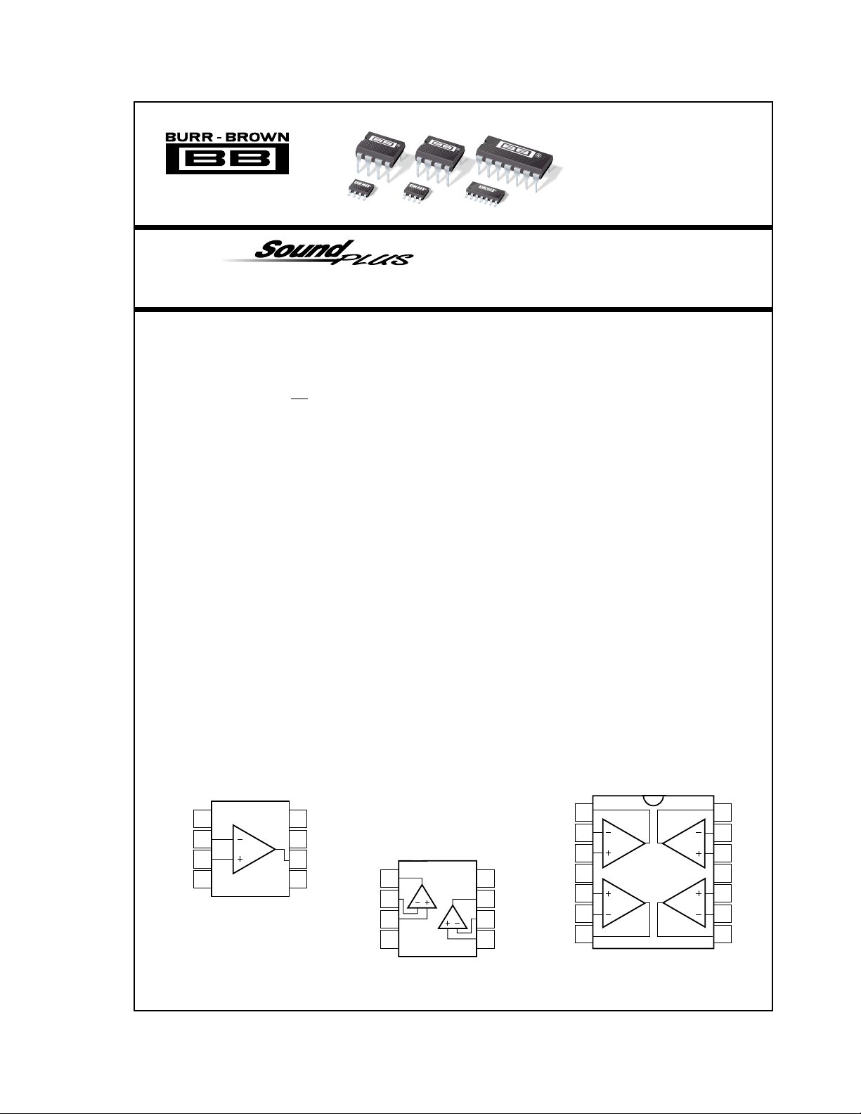
BURR-BROWN OPA134, OPA2134, OPA4134 User Manual
®
OPA134
OPA134
OPA2134
OPA2134
OPA4134
OPA4134
OPA134
OPA2134
OPA4134
High Performance
TM
AUDIO OPERATIONAL AMPLIFIERS
FEATURES
● SUPERIOR SOUND QUALITY
● ULTRA LOW DISTORTION: 0.00008%
● LOW NOISE: 8nV/√Hz
● TRUE FET-INPUT: I
= 5pA
B
● HIGH SPEED:
SLEW RATE: 20V/µs
BANDWIDTH: 8MHz
● HIGH OPEN-LOOP GAIN: 120dB (600Ω)
● WIDE SUPPLY RANGE:
±2.5V to ±18V
● SINGLE, DUAL, AND QUAD VERSIONS
APPLICATIONS
● PROFESSIONAL AUDIO AND MUSIC
● LINE DRIVERS
● LINE RECEIVERS
● MULTIMEDIA AUDIO
● ACTIVE FILTERS
● PREAMPLIFIERS
● INTEGRATORS
● CROSSOVER NETWORKS
OPA134
Offset Trim
International Airport Industrial Park • Mailing Address: PO Box 11400, Tucson, AZ 85734 • Street Address: 6730 S. Tucson Blvd., Tucson, AZ 85706 • Tel: (520) 746-1111 • Twx: 910-952-1111
1
2
–In
3
+In
4
V–
8-Pin DIP, SO-8
Internet: http://www.burr-brown.com/ • FAXLine: (800) 548-6133 (US/Canada Only) • Cable: BBRCORP • Telex: 066-6491 • FAX: (520) 889-1510 • Immediate Product Info: (800) 548-6132
8
7
6
5
Offset Trim
V+
Output
NC
Out A
–In A
+In A
OPA2134
1
A
2
3
4
V–
8-Pin DIP, SO-8
DESCRIPTION
The OPA134 series are ultra-low distortion, low noise
operational amplifiers fully specified for audio applications. A true FET input stage was incorporated to
provide superior sound quality and speed for exceptional audio performance. This in combination with
high output drive capability and excellent dc performance allows use in a wide variety of demanding
applications. In addition, the OPA134’s wide output
swing, to within 1V of the rails, allows increased
headroom making it ideal for use in any audio circuit.
OPA134 op amps are easy to use and free from phase
inversion and overload problems often found in common FET-input op amps. They can be operated from
±2.5V to ±18V power supplies. Input cascode cir-
cuitry provides excellent common-mode rejection and
maintains low input bias current over its wide input
voltage range, minimizing distortion. OPA134 series
op amps are unity-gain stable and provide excellent
dynamic behavior over a wide range of load conditions, including high load capacitance. The dual and
quad versions feature completely independent circuitry for lowest crosstalk and freedom from interaction, even when overdriven or overloaded.
Single and dual versions are available in 8-pin DIP
and SO-8 surface-mount packages in standard configurations. The quad is available in 14-pin DIP and
SO-14 surface mount packages. All are specified for
–40°C to +85°C operation. A SPICE macromodel is
available for design analysis.
OPA4134
1
Out A
2
–In A
+In A
V+
8
Out B
7
B
–In B
6
+In B
5
V+
+In B
–In B
Out B
AD
3
4
5
BC
6
7
14-Pin DIP
SO-14
Out D
14
–In D
13
+In D
12
V–
11
+In C
10
–In C
9
Out C
8
SBOS058
© 1996 Burr-Brown Corporation PDS-1339C Printed in U.S.A. December, 1997
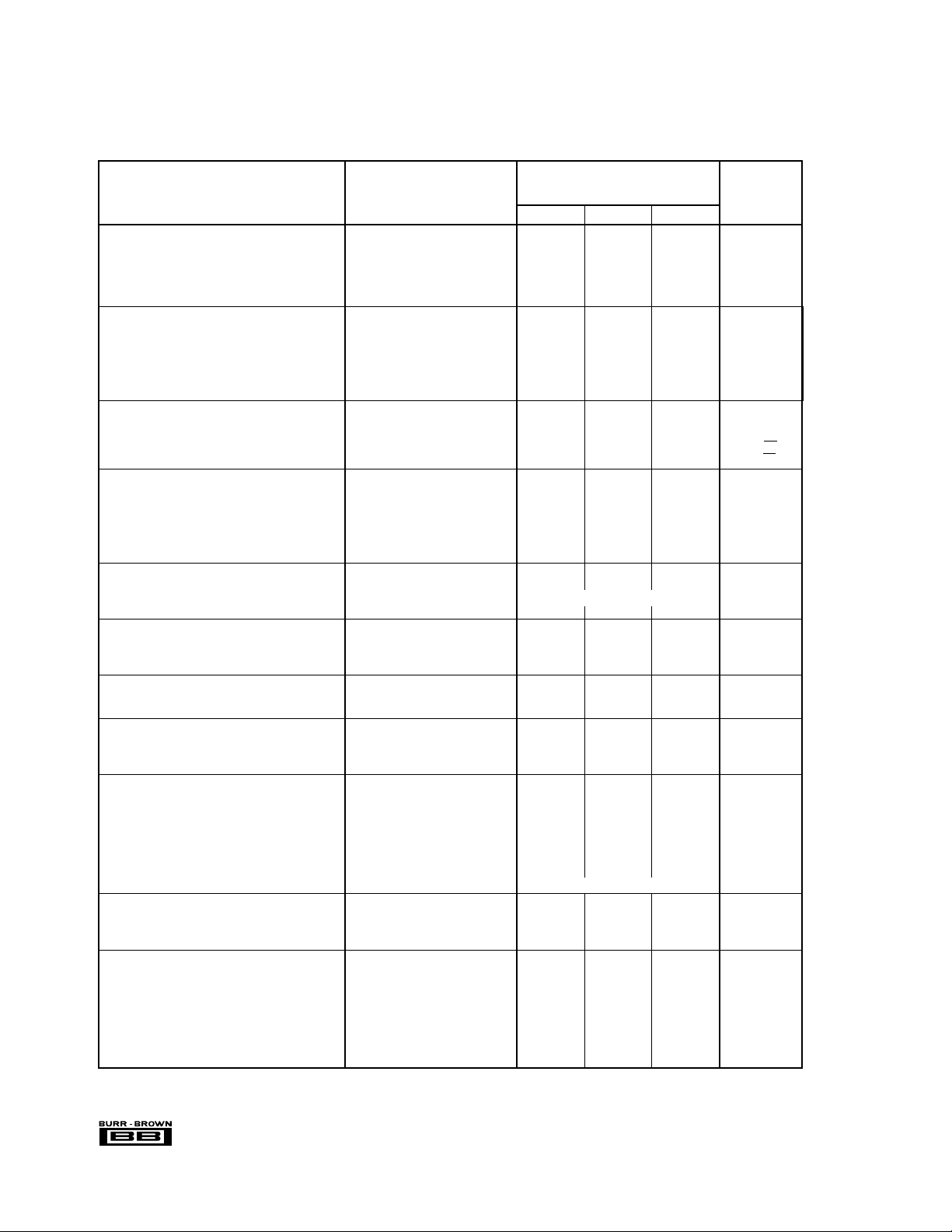
SPECIFICATIONS
At TA = +25°C, VS = ±15V, unless otherwise noted.
OPA134PA, UA
OPA2134PA, UA
OPA4134PA, UA
PARAMETER CONDITION MIN TYP MAX UNITS
AUDIO PERFORMANCE
Total Harmonic Distortion + Noise G = 1, f = 1kHz, V
Intermodulation Distortion G = 1, f = 1kHz, V
(1)
Headroom
THD < 0.01%, RL = 2kΩ, VS = ±18V 23.6 dBu
FREQUENCY RESPONSE
Gain-Bandwidth Product 8 MHz
(2)
Slew Rate
Full Power Bandwidth 1.3 MHz
Settling Time 0.1% G = 1, 10V Step, C
Overload Recovery Time (V
0.01% G = 1, 10V Step, C
IN
NOISE
Input Voltage Noise
Noise Voltage, f = 20Hz to 20kHz 1.2 µVrms
Noise Density, f = 1kHz 8 nV/√Hz
Current Noise Density, f = 1kHz 3 fA/√Hz
OFFSET VOLTAGE
Input Offset Voltage ±0.5 ±2mV
T
= –40°C to +85°C ±1 ±3
vs Temperature T
vs Power Supply (PSRR) V
Channel Separation (Dual, Quad) dc, R
A
= –40°C to +85°C ±2 µV/°C
A
= ±2.5V to ±18V 90 106 dB
S
f = 20kHz, R
INPUT BIAS CURRENT
Input Bias Current
vs Temperature
Input Offset Current
(4)
(3)
(4)
INPUT VOLTAGE RANGE
Common-Mode Voltage Range (V–)+2.5 ±13 (V+)–2.5 V
Common-Mode Rejection V
= –12.5V to +12.5V 86 100 dB
CM
T
= –40°C to +85°C90dB
A
INPUT IMPEDANCE
Differential 10
Common-Mode V
= –12.5V to +12.5V 1013 || 5 Ω || pF
CM
OPEN-LOOP GAIN
Open-Loop Voltage Gain R
= 10kΩ, VO = –14.5V to +13.8V 104 120 dB
L
R
= 2kΩ, VO = –13.8V to +13.5V 104 120 dB
L
R
= 600Ω, VO = –12.8V to +12.5V 104 120 dB
L
OUTPUT
Voltage Output R
Output Current ±35 mA
Output Impedance, Closed-Loop
(5)
Open-Loop f = 10kHz 10 Ω
Short-Circuit Current ±40 mA
Capacitive Load Drive (Stable Operation) See Typical Curve
POWER SUPPLY
Specified Operating Voltage ±15 V
Operating Voltage Range ±2.5 ±18 V
Quiescent Current (per amplifier) I
TEMPERATURE RANGE
Specified Range –40 +85 °C
Operating Range –55 +125 °C
Storage –55 +125 °C
Thermal Resistance,
8-Pin DIP 100 °C/W
θ
JA
SO-8 Surface-Mount 150 °C/W
14-Pin DIP 80 °C/W
SO-14 Surface-Mount 110 °C/W
NOTES: (1) dBu = 20*log (Vrms/0.7746) where Vrms is the maximum output voltage for which THD+Noise is less than 0.01%. See THD+Noise text. (2) Guaranteed
by design. (3) Guaranteed by wafer-level test to 95% confidence level. (4) High-speed test at T
typical curve.
®
OPA134/2134/4134
= 3Vrms
O
R
= 2kΩ 0.00008 %
L
R
= 600Ω 0.00015 %
L
= 1Vp-p –98 dB
O
±15 ±20 V/µs
= 100pF 0.7 µs
L
= 100pF 1 µs
L
) • (Gain) = V
S
= 2kΩ 135 dB
L
= 2kΩ 130 dB
L
0.5 µs
(3)
VCM =0V +5 ±100 pA
See Typical Curve ±5nA
VCM =0V ±2 ±50 pA
13
|| 2 Ω || pF
= 10kΩ (V–)+0.5 (V+)–1.2 V
L
R
= 2kΩ (V–)+1.2 (V+)–1.5 V
L
R
= 600Ω (V–)+2.2 (V+)–2.5 V
L
f = 10kHz 0.01 Ω
= 0 4 5 mA
O
= 25°C. (5) See “Closed-Loop Output Impedance vs Frequency”
J
2
mV
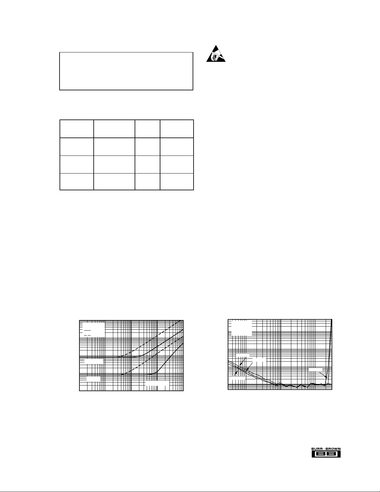
ABSOLUTE MAXIMUM RATINGS
Supply Voltage, V+ to V– .................................................................... 36V
Input Voltage .................................................... (V–) –0.7V to (V+) +0.7V
Output Short-Circuit
Operating Temperature ................................................. –40°C to +125°C
Storage Temperature ..................................................... –55°C to +125°C
Junction Temperature ...................................................................... 150° C
Lead Temperature (soldering, 10s)................................................. 300°C
NOTES: (1) Stresses above these ratings may cause permanent damage.
(2) Short-circuit to ground, one amplifier per package.
(2)
.............................................................. Continuous
(1)
PACKAGE/ORDERING INFORMATION
PACKAGE
DRAWING TEMPERATURE
PRODUCT PACKAGE NUMBER
Single
OPA134PA 8-Pin Plastic DIP 006 –40°C to +85°C
OPA134UA SO-8 Surface-Mount 182 –40°C to +85°C
Dual
OPA2134PA 8-Pin Plastic DIP 006 –40°C to +85°C
OPA2134UA SO-8 Surface-Mount 182 –40°C to +85°C
Quad
OPA4134PA 14-Pin Plastic DIP 010 –40°C to +85°C
OPA4134UA SO-14 Surface-Mount 235 –40°C to +85°C
NOTE: (1) For detailed drawing and dimension table, please see end of data
sheet, or Appendix C of Burr-Brown IC Data Book.
(1)
RANGE
ELECTROSTATIC
DISCHARGE SENSITIVITY
This integrated circuit can be damaged by ESD. Burr-Brown
recommends that all integrated circuits be handled with
appropriate precautions. Failure to observe proper handling
and installation procedures can cause damage.
ESD damage can range from subtle performance degradation to complete device failure. Precision integrated circuits
may be more susceptible to damage because very small
parametric changes could cause the device not to meet its
published specifications.
TYPICAL PERFORMANCE CURVES
At TA = +25°C, VS = ±15V, RL = 2kΩ, unless otherwise noted.
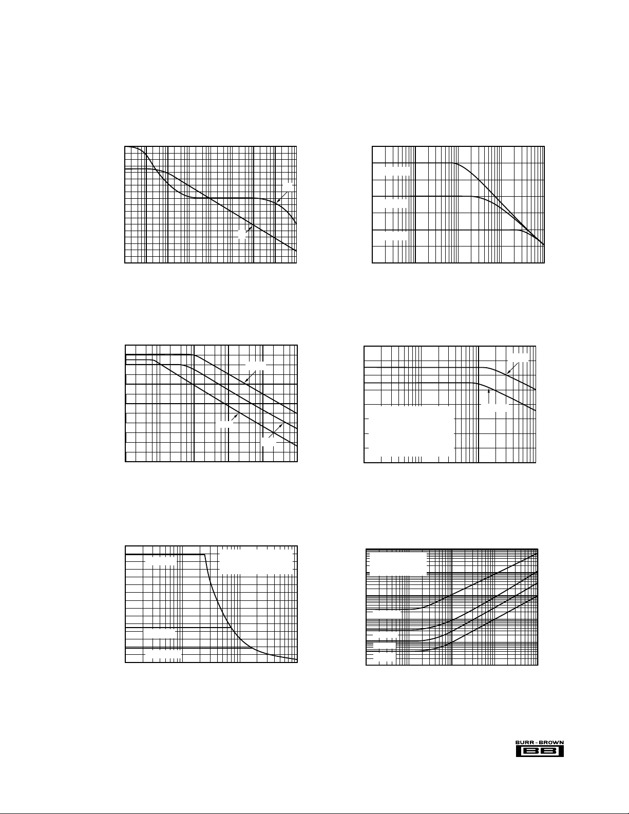
TOTAL HARMONIC DISTORTION + NOISE
0.1
0.01
0.001
THD+Noise (%)
0.0001
0.00001
The information provided herein is believed to be reliable; however, BURR-BROWN assumes no responsibility for inaccuracies or omissions. BURR-BROWN assumes
no responsibility for the use of this information, and all use of such information shall be entirely at the user’s own risk. Prices and specifications are subject to change
without notice. No patent rights or licenses to any of the circuits described herein are implied or granted to any third party. BURR-BROWN does not authorize or warrant
any BURR-BROWN product for use in life support devices and/or systems.
R
L
2kΩ
600Ω
G = +10
G = +1
10 100 1k 10k 100k
vs FREQUENCY
Frequency (Hz)
VO = 3Vrms
0.1
IMD (%)
0.010
0.001
0.0005
3 OPA134/2134/4134
SMPTE INTERMODULATION DISTORTION
5
1
30m
G = +1
f = 1kHz
= 2kΩ
R
L
OPA134
Baseline
vs OUTPUT AMPLITUDE
OP176
0.1 1
Output Amplitude (Vpp)
OPA134
10 30
®
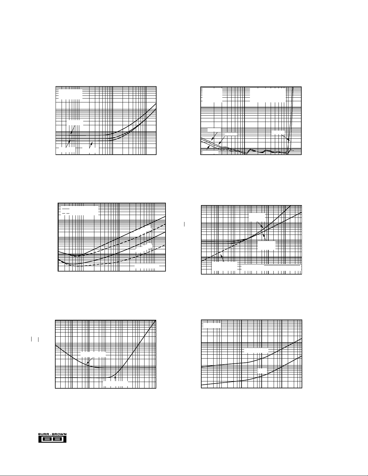
HEADROOM – TOTAL HARMONIC DISTORTION
+ NOISE vs OUTPUT AMPLITUDE
Output Amplitude (Vrms)
THD+Noise (%)
1
0.1
0.010
0.001
0.0005
0.1
1
10 20
VS = ±18V
R
L
= 2kΩ
f = 1kHz
THD < 0.01%
OPA134 – 11.7Vrms
OP176 – 11.1Vrms
Baseline
OP176
OPA134
OPA134
TYPICAL PERFORMANCE CURVES (CONT)
At TA = +25°C, VS = ±15V, RL = 2kΩ, unless otherwise noted.
TOTAL HARMONIC DISTORTION + NOISE
0.01
VO = 10Vrms
= 2kΩ
R
L
0.001
VS = ±16
0.0001
THD+Noise (%)
0.00001
0.00001
VS = ±17
20 100 1k 10k 20k
HARMONIC DISTORTION + NOISE vs FREQUENCY
0.01
2nd Harmonic
3rd Harmonic
0.001
0.0001
vs FREQUENCY
VS = ±18
Frequency (Hz)
Amplitude (% of Fundamentals)
0.000001
20 100 1k 10k 20k
Frequency (Hz)
= 600Ω
L
R
= 2kΩ
L
R
VO = 1Vrms
VOLTAGE NOISE vs SOURCE RESISTANCE
1k
OP176+
100
10
Resistor
OPA134+
Resistor
1
Voltage Noise (nV/√Hz)
Resistor Noise
Only
Vn (total) = √(inRS)2 + e
0.1
10 100 1k 10k 100k 1M 10M
Source Resistance (Ω)
2
+ 4kTR
n
S
INPUT VOLTAGE AND CURRENT NOISE
1k
100
10
Current Noise (fA/√Hz)
Voltage Noise (nV/√Hz)
1
SPECTRAL DENSITY vs FREQUENCY
Voltage Noise
10 100 1k 10k 100k 1M
1
®
Frequency (Hz)
OPA134/2134/4134
Current Noise
INPUT-REFERRED NOISE VOLTAGE
100
RS = 20Ω
10
1
Noise Voltage (µV)
0.1
1 10 100 1k 10k 100k
vs NOISE BANDWIDTH
Peak-to-Peak
RMS
Noise Bandwidth (Hz)
4
TYPICAL PERFORMANCE CURVES (CONT)
At TA = +25°C, VS = ±15V, RL = 2kΩ, unless otherwise noted.
160
140
120
100
80
60
40
Voltage Gain (dB)
20
–20
120
100
80
60
40
PSR, CMR (dB)
20
OPEN-LOOP GAIN/PHASE vs FREQUENCY
G
0
0.1 1 10 100 1k 10k 100k 1M 10M
Frequency (Hz)
POWER SUPPLY AND COMMON-MODE REJECTION
vs FREQUENCY
–PSR
+PSR
0
10 100 1k 10k 100k 1M
Frequency (Hz)
CMR
0
–45
φ
–90
–135
Phase Shift (°)
–180
50
40
30
20
10
0
Closed-Loop Gain (dB)
–10
–20
1k 10k 100k 1M 10M
160
140
120
Dual and quad devices.
G = 1, all channels.
Quad measured channel
100
A to D or B to C—other
Channel Separation (dB)
combinations yield improved
rejection.
80
100 1k 10k 100k
CLOSED-LOOP GAIN vs FREQUENCY
G = +100
G = +10
G = +1
Frequency (Hz)
CHANNEL SEPARATION vs FREQUENCY
RL = ∞
RL = 2kΩ
Frequency (Hz)
MAXIMUM OUTPUT VOLTAGE
30
VS = ±15V
20
10
Output Voltage (Vp-p)
VS = ±5V
0
VS = ±2.5V
10k 100k 1M 10M
vs FREQUENCY
Maximum output voltage
without slew-rate
induced distortion
Frequency (Hz)
CLOSED-LOOP OUTPUT IMPEDANCE vs FREQUENCY
10
Note: Open-Loop
Output Impedance
1
at f = 10kHz is 10Ω
0.1
G = +100
0.01
G = +10
0.001
G = +2
Closed-Loop Output Impedance (Ω)
0.0001
G = +1
10 100 1k 10k 100k
Frequency (Hz)
5 OPA134/2134/4134
®
 Loading...