

BURR-BROWN OPA130, OPA2130, OPA4130 User Manual
查询OPA130供应商
®
OPA130
OPA130
Low Power, Precision
FET-INPUT OPERATIONAL AMPLIFIERS
FEATURES
● LOW QUIESCENT CURRENT: 530µA/amp
● LOW OFFSET VOLTAGE: 1mV max
● HIGH OPEN-LOOP GAIN: 120dB min
● HIGH CMRR: 90 dB min
● FET INPUT: I
● EXCELLENT BANDWIDTH: 1MHz
● WIDE SUPPLY RANGE: ±2.25 to ±18V
● SINGLE, DUAL, AND QUAD VERSIONS
= 20pA max
B
OPA2130
OPA2130
OPA4130
OPA4130
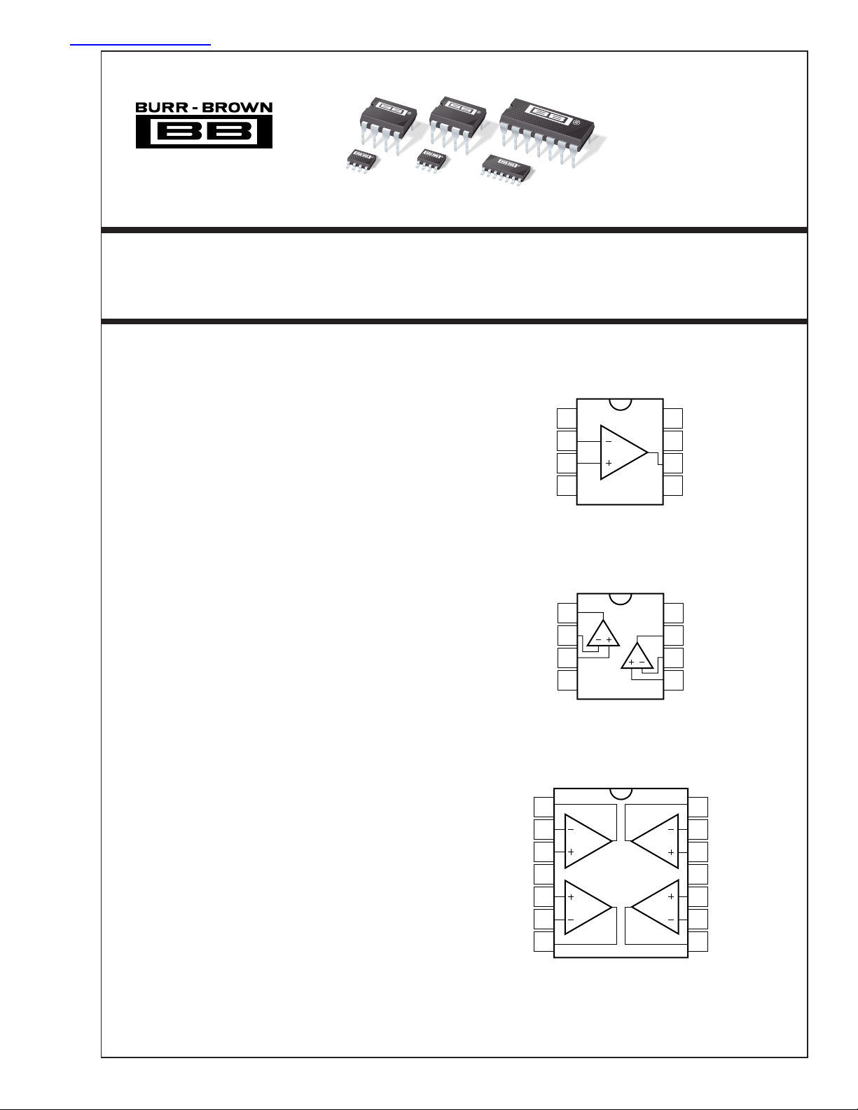
Offset Trim
–In
+In
V–
1
2
3
4
8-Pin DIP, SO-8
OPA130
OPA130
OPA2130
OPA4130
NC
8
V+
7
Output
6
Offset Trim
5
DESCRIPTION
The OPA130 series of FET-input op amps combine
precision dc performance with low quiescent current.
Single, dual, and quad versions have identical specifications for maximum design flexibility. They are ideal
for general-purpose, portable, and battery operated
applications, especially with high source impedance.
OPA130 op amps are easy to use and free from phase
inversion and overload problems often found in
common FET-input op amps. Input cascode circuitry
provides excellent common-mode rejection and
maintains low input bias current over its wide input
voltage range. OPA130 series op amps are stable in
unity gain and provide excellent dynamic behavior
over a wide range of load conditions, including high
load capacitance. Dual and quad designs feature
completely independent circuitry for lowest crosstalk
and freedom from interaction, even when overdriven
or overloaded.
Single and dual versions are available in 8-pin DIP
and SO-8 surface-mount packages. Quad is
available in 14-pin DIP and SO-14 surface-mount
packages. All are specified for –40°C to +85°C
operation.
Out A
–In A
+In A
V+
+In B
–In B
Out B
Out A
–In A
+In A
V–
OPA2130
1
A
2
3
4
8-Pin DIP, SO-8
1
2
3
4
5
6
7
AD
BC
14-Pin DIP
B
OPA4130
SO-14
V+
8
Out B
7
–In B
6
+In B
5
Out D
14
–In D
13
+In D
12
V–
11
+In C
10
–In C
9
Out C
8
International Airport Industrial Park • Mailing Address: PO Box 11400, Tucson, AZ 85734 • Street Address: 6730 S. Tucson Blvd., Tucson, AZ 85706 • Tel: (520) 746-1111 • Twx: 910-952-1111
Internet: http://www.burr-brown.com/ • FAXLine: (800) 548-6133 (US/Canada Only) • Cable: BBRCORP • Telex: 066-6491 • FAX: (520) 889-1510 • Immediate Product Info: (800) 548-6132
© 1995 Burr-Brown Corporation PDS-1298B Printed in U.S.A. May, 1998

SPECIFICATIONS
At TA = +25°C, VS = ±15V, and RL = 10kΩ, unless otherwise noted.
OPA130PA, UA
OPA2130PA, UA
OPA4130PA, UA
PARAMETER CONDITION MIN TYP MAX UNITS
OFFSET VOLTAGE
Input Offset Voltage ±0.2 ±1mV
vs Temperature
vs Power Supply V
Channel Separation (dual and quad) 0.3 µV/V
INPUT BIAS CURRENT
Input Bias Current VCM = 0V +5 ±10 pA
vs Temperature See Typical Curve
Input Offset Current V
NOISE
Input Voltage Noise
Noise Density, f = 10Hz 30 nV/√Hz
Current Noise Density, f = 1kHz 4 fA/√Hz
INPUT VOLTAGE RANGE
Common-Mode Voltage Range, Positive (V+)–2 (V+)–1.5 V
Common-Mode Rejection V
INPUT IMPEDANCE
Differential 1013 || 1 Ω || pF
Common-Mode V
OPEN-LOOP GAIN
Open-loop Voltage Gain V
FREQUENCY RESPONSE
Gain-Bandwidth Product 1 MHz
Slew Rate 2V/µs
Settling Time: 0.1% G = 1, 10V Step, C
Overload Recovery Time G = 1, V
Total Harmonic Distortion + Noise 1kHz, G = 1, V
OUTPUT
Voltage Output, Positive (V+)–2 (V+)–1.5 V
Short-Circuit Current ±18 mA
Capacitive Load Drive (Stable Operation) 10 nF
POWER SUPPLY
Specified Operating Voltage ±15 V
Operating Voltage Range ±2.25 ±18 V
Quiescent Current (per amplifier) I
TEMPERATURE RANGE
Operating Range –40 +85 °C
Storage –40 +125 °C
Thermal Resistance,
8-Pin DIP 100 °C/W
SO-8 Surface-Mount 150 °C/W
14-Pin DIP 80 °C/W
SO-14 Surface-Mount 110 °C/W
NOTES: (1) Guaranteed by wafer test. (2) High-speed test at T
(1)
(2)
Operating Temperature Range ±2 ±10 µV/° C
= ±2.25V to ±18V 2 20 µV/V
S
= 0V ±2 ±20 pA
CM
f = 100Hz 18 nV/√Hz
f = 1kHz 16 nV/√Hz
f = 10kHz 16 nV/√Hz
Negative (V–)+2 (V–)+1.2 V
= –13V to +13V 90 105 dB
CM
= –13V to +13V 1013 || 3 Ω || pF
CM
= –13.8V to +13V 120 135 dB
O
= 2kΩ, VO = –13V to +12V 120 135 dB
R
L
= 100pF 5.5 µs
L
0.01% G = 1, 10V Step, C
= 100pF 7 µs
L
= ±15V 2 µs
IN
= 3.5Vrms 0.0003 %
O
Negative (V–)+1.2 (V–)+1 V
Positive R
Negative R
θ
JA
= 25°C.
J
= 2kΩ (V+)–3 (V+)–2.5 V
L
= 2kΩ (V–)+2 (V–)+1.5 V
L
= 0 ±530 ±650 µA
O
The information provided herein is believed to be reliable; however, BURR-BROWN assumes no responsibility for inaccuracies or omissions. BURR-BROWN assumes
no responsibility for the use of this information, and all use of such information shall be entirely at the user’s own risk. Prices and specifications are subject to change
without notice. No patent rights or licenses to any of the circuits described herein are implied or granted to any third party. BURR-BROWN does not authorize or warrant
any BURR-BROWN product for use in life support devices and/or systems.
®
OPA130, 2130, 4130
2
ABSOLUTE MAXIMUM RATINGS
Supply Voltage, V+ to V–....................................................................36V
Input Voltage .................................................... (V–) –0.7V to (V+) +0.7V
Output Short-Circuit
Operating Temperature ................................................. –40°C to +125°C
Storage Temperature ..................................................... –40°C to +125°C
Junction Temperature...................................................................... 150°C
Lead Temperature (soldering, 10s)................................................. 300°C
NOTE: (1) Short-circuit to ground, one amplifier per package.
(1)
.............................................................. Continuous
PACKAGE/ORDERING INFORMATION
PACKAGE
DRAWING TEMPERATURE
(1)
PRODUCT PACKAGE NUMBER
Single
OPA130PA 8-Pin Plastic DIP 006 –40°C to +85°C
OPA130UA SO-8 Surface-Mount 182 –40°C to +85°C
Dual
OPA2130PA 8-Pin Plastic DIP 006 –40°C to +85°C
OPA2130UA SO-8 Surface-Mount 182 –40°C to +85°C
Quad
OPA4130PA 14-Pin Plastic DIP 010 –40°C to +85°C
OPA4130UA SO-14 Surface-Mount 235 –40°C to +85°C
NOTE: (1) For detailed drawing and dimension table, please see end of data
sheet, or Appendix C of Burr-Brown IC Data Book.
RANGE
ELECTROSTATIC
DISCHARGE SENSITIVITY
This integrated circuit can be damaged by ESD. Burr-Brown
recommends that all integrated circuits be handled with
appropriate precautions. Failure to observe proper handling
and installation procedures can cause damage.
ESD damage can range from subtle performance degradation to complete device failure. Precision integrated circuits
may be more susceptible to damage because very small
parametric changes could cause the device not to meet its
published specifications.
®
3
OPA130, 2130, 4130
 Loading...