

BURR-BROWN OPA350, OPA2350, OPA4350 User Manual
OPA2350
Please be aware that an important notice concerning availability, standard warranty, and use in critical applications of Texas Instruments
OPA4350
SBOS099C − SEPTEMBER 2000 − REVISED JANUARY 2005
High-Speed, Single-Supply, Rail-to-Rail
OPERATIONAL AMPLIFIERS
MicroAmplifiertSeries
OPA350
FEATURES
D RAIL-TO-RAIL INPUT
D RAIL-TO-RAIL OUTPUT (within 10mV)
D WIDE BANDWIDTH: 38MHz
D HIGH SLEW RATE: 22V/µs
D LOW NOISE: 5nV/√Hz
D LOW THD+NOISE: 0.0006%
D UNITY-GAIN STABLE
D MicroSIZE PACKAGES
D SINGLE, DUAL, AND QUAD
APPLICATIONS
D CELL PHONE PA CONTROL LOOPS
D DRIVING A/D CONVERTERS
D VIDEO PROCESSING
D DATA ACQUISITION
D PROCESS CONTROL
D AUDIO PROCESSING
D COMMUNICATIONS
D ACTIVE FILTERS
D TEST EQUIPMENT
DESCRIPTION
The OPA350 series rail-to-rail CMOS operational
amplifiers are optimized for low voltage, single-supply
operation. Rail-to-rail input/output, low noise (5nV/√Hz
and high speed operation (38MHz, 22V/µs) make them
ideal for driving sampling Analog-to-Digital (A/D)
converters. They are also well suited for cell phone PA
control loops and video processing (75Ω drive capability)
as well as audio and general purpose applications. Single,
dual, and quad versions have identical specifications for
maximum design flexibility.
The OPA350 series operates on a single supply as low as
2.5V with an input common-mode voltage range that
extends 300mV below ground and 300mV above the
positive supply. Output voltage swing is to within 10mV of
the supply rails with a 10kΩ load. Dual and quad designs
feature completely independent circuitry for lowest
crosstalk and freedom from interaction.
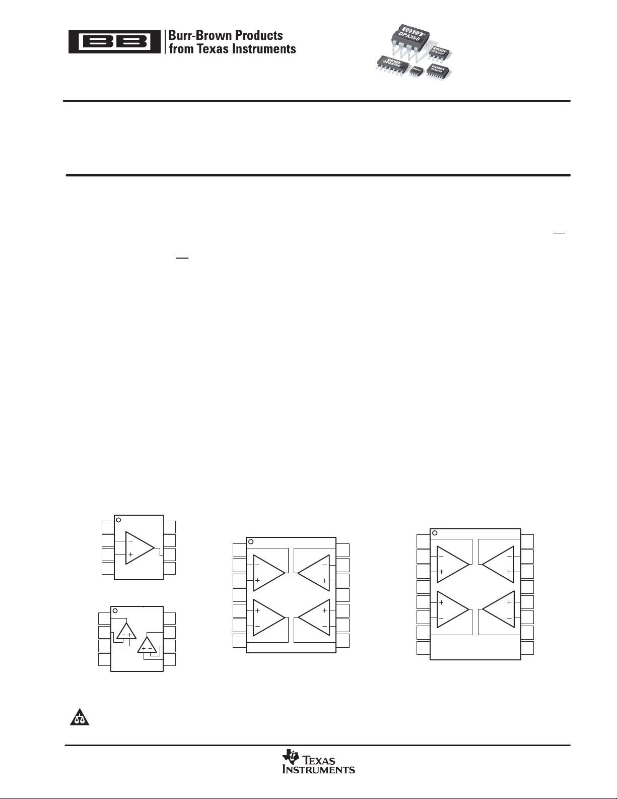
The single (OPA350) and dual (OPA2350) come in the
miniature MSOP-8 surface mount, SO-8 surface mount,
and DIP-8 packages. The quad (OPA4350) packages are
the space-saving SSOP-16 surface mount and SO-14
surface mount. All a r e s p e c i f i e d f r o m − 4 0 °C to +85°C and
operate from −55°C to +150°C.
),
OPA350
1
NC
2
−In
3
+In
−
4
V
DIP−8, SO−8, MSOP−8
OPA2350
1
OutA
A
2
−In A
3
+In A
−
4
DIP−8, SO−8, MSOP−8
semiconductor products and disclaimers thereto appears at the end of this data sheet.
All trademarks are the property of their respective owners.
! !
B
NC
8
V+
7
Output
6
NC
5
8
V+
7
Out B
6
−In B
5
+In B
Out A
−In A
+In A
V+
+In B
−In B
Out B
1
2
3
4
5
6
7
OPA4350
AD
BC
SO−14
SPICE model available at www.ti.com
Out A
−In A
+In A
+V
+In B
−In B
Out B
NC
Copyright 2000−2005, Texas Instruments Incorporated
www.ti.com
14
Out D
13
−In D
12
+In D
11
V
−
10
+In C
9
−In C
8
Out C
OPA4350
1
2
AD
3
4
5
BC
6
7
8
SSOP−16
16
Out D
15
−In D
14
+In D
−
13
V
12
+In C
11
−In C
10
Out C
9
NC
"#$
OPA350EA
MSOP-8
DGK
−40°C to +85°C
C50
OPA350UA
SO-8
D
−40°C to +85°C
OPA350UA
OPA2350EA
MSOP-8
DGK
−40°C to +85°C
D50
OPA2350UA
SO-8
D
−40°C to +85°C
OPA2350UA
OPA4350EA
SSOP-16
DBQ
−40°C to +85°C
OPA4350EA
OPA4350UA
SO-14
D
−40°C to +85°C
OPA4350UA
%"#$
&"#$
SBOS099C − SEPTEMBER 2000 − REVISED JANUARY 2005
www.ti.com
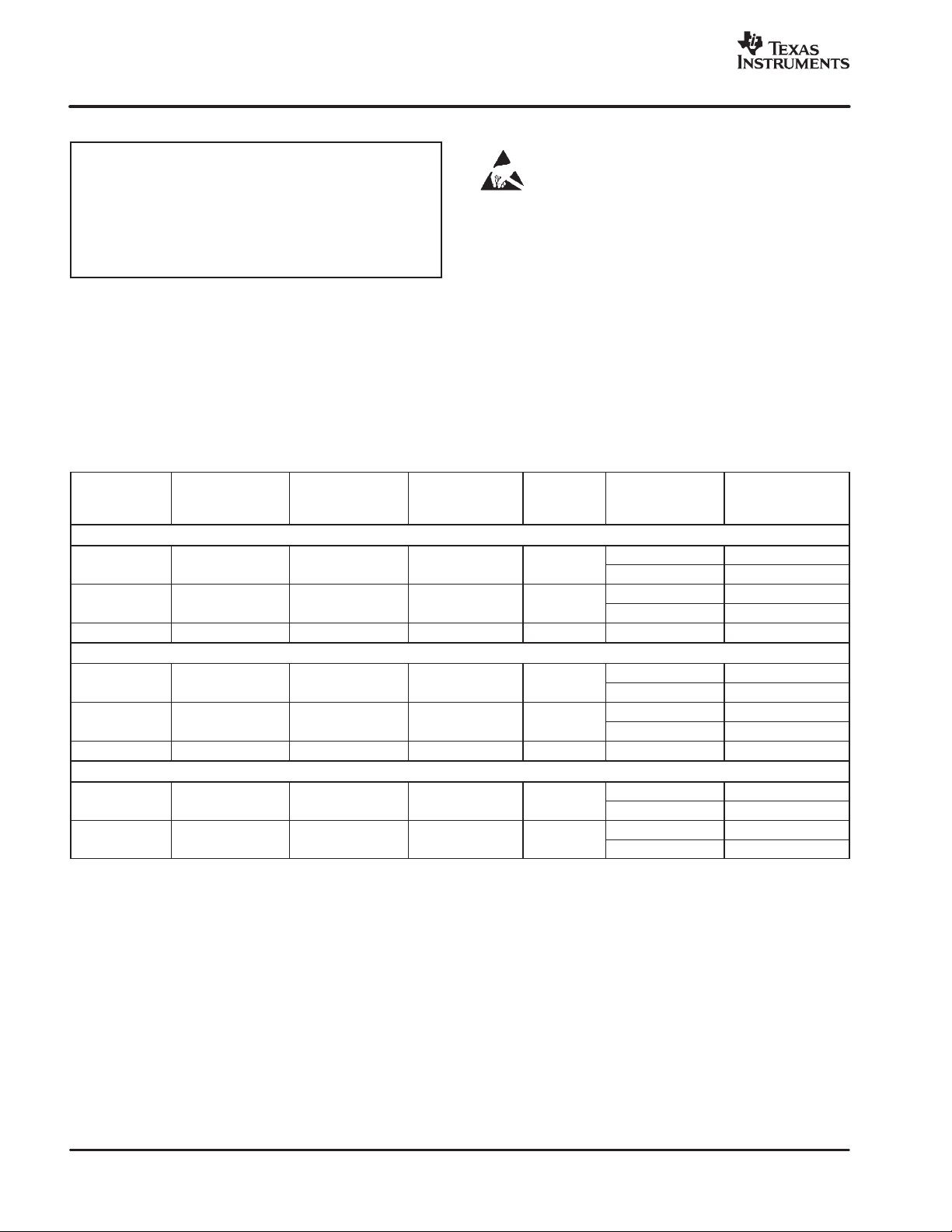
ABSOLUTE MAXIMUM RATINGS
Supply Voltage 7.0V. . . . . . . . . . . . . . . . . . . . . . . . . . . . . . . . . . . . . .
Signal Input Terminals
Open Short-Circuit Current
Operating Temperature Range −55°C to +150°C. . . . . . . . . . . . . . .
Storage Temperature Range −55°C to +150°C. . . . . . . . . . . . . . . . .
Junction Temperature +150°C. . . . . . . . . . . . . . . . . . . . . . . . . . . . . . .
Lead Tem perature (soldering, 10s) +300°C. . . . . . . . . . . . . . . . . . . . .
(1)
Stresses above these ratings may cause permanent damage.
Exposure to absolute maximum conditions for extended periods
may degrade device reliability. These are stress ratings only , an d
functional operation of the device at these or any other conditions
beyond those specified is not implied.
(2)
Input terminals are diode-clamped to the power-supply rails.
Input signals that can swing more than 0.3V beyond the supply
rails should be current limited to 10mA or less.
(3)
Short-circuit to ground, one amplifier per package.
(2)
,Voltage (V−) − 0.3V to (V+) + 0.3V. . . . .
Current 10mA. . . . . . . . . . . . . . . . . . . . . .
(3)
PACKAGE/ORDERING INFORMATION
PRODUCT PACKAGE-LEAD
SINGLE
OPA350PA DIP-8 P −40°C to +85°C OPA350PA OPA350PA Rails
DUAL
OPA2350PA DIP-8 P −40°C to +85°C OPA2350PA OPA2350PA Rails
QUAD
(1)
For the most current package and ordering information, see the Package Option Addendum located at the end of this data sheet.
(1)
Continuous. . . . . . . . . . . . . . . . . . . .
PACKAGE
DESIGNATOR
(1)
TEMPERATURE
ELECTROSTATIC DISCHARGE SENSITIVITY
This integrated circuit can be damaged by ESD. Texas
Instruments recommends that all integrated circuits be
handled with appropriate precautions. Failure to observe
proper handling and installation procedures can cause damage.
ESD damage can range from subtle performance degradation to
complete device failure. Precision integrated circuits may be more
susceptible t o damage because very small parametric changes could
cause the device not to meet its published specifications.
SPECIFIED
RANGE
PACKAGE
MARKING
ORDERING
NUMBER
OPA350EA/250 Tape and Reel, 250
OPA350EA/2K5 Tape and Reel, 2500
OPA350UA Rails
OPA350UA/2K5 Tape and Reel, 2500
OPA2350EA/250 Tape and Reel, 250
OPA2350EA/2K5 Tape and Reel, 2500
OPA2350UA Rails
OPA2350UA/2K5 Tape and Reel, 2500
OPA4350EA/250 Tape and Reel, 250
OPA4350EA/2K5 Tape and Reel, 2500
OPA4350UA Rails
OPA4350UA/2K5 Tape and Reel, 2500
MEDIA, QUANTITY
TRANSPORT
2
"#$
%"#$
www.ti.com
SBOS099C − SEPTEMBER 2000 − REVISED JANUARY 2005
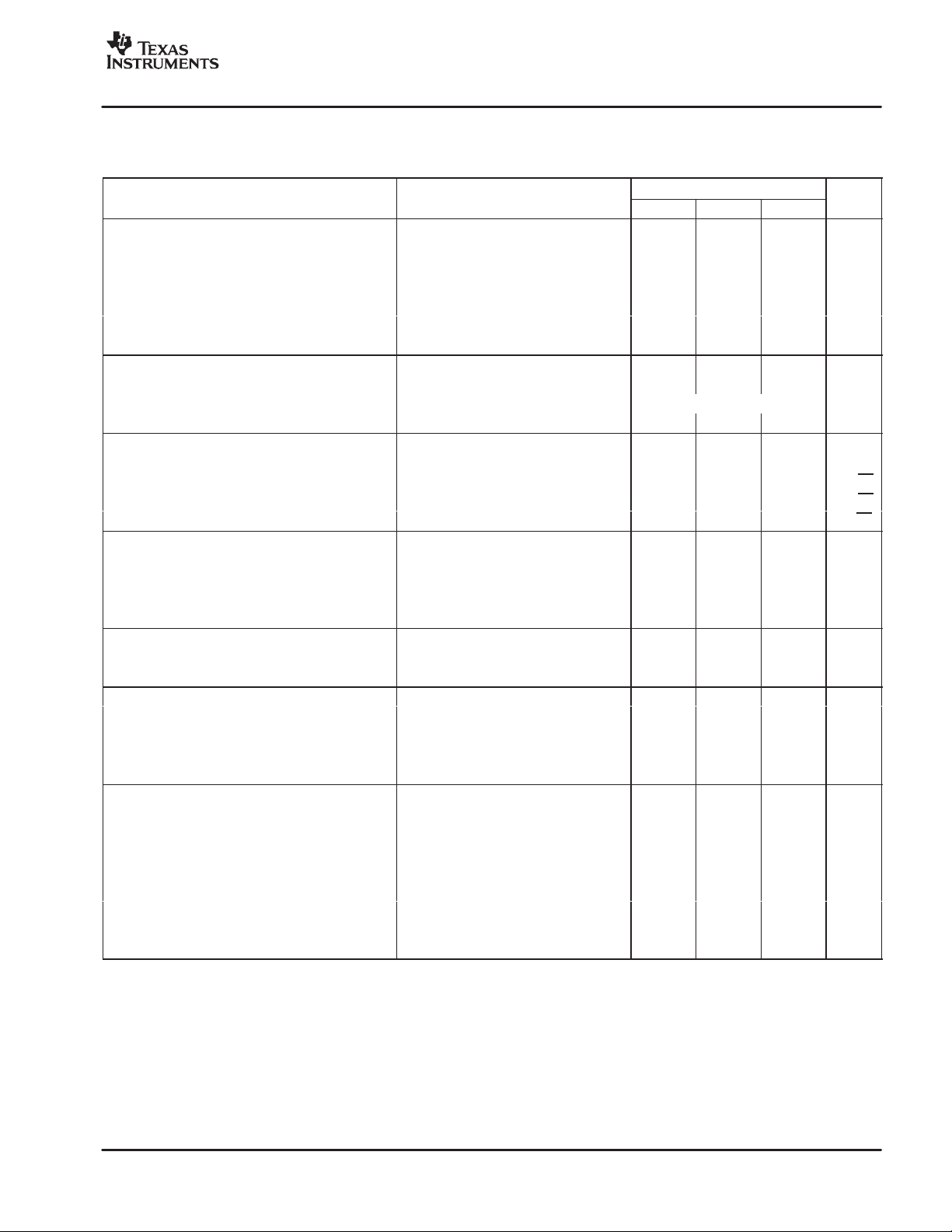
ELECTRICAL CHARACTERISTICS: VS = 2.7V to 5.5V
Boldface limits apply over the temperature range, TA = −40°C to +85°C. VS = 5V.
All specifications at TA = +25°C, RL = 1kΩ connected to VS/2 and V
PARAMETER TEST CONDITIONS MIN TYP
OFFSET VOLTAGE
Input Offset Voltage V
TA = −40°C to +85°C ±1 mV
vs Temperature TA = −40°C to +85°C ±4 µV/°C
vs Power-Supply Rejection Ratio PSRR VS = 2.7V to 5.5V , VCM = 0V 40 150 µV/V
TA = −40°C to +85°C VS = 2.7V to 5.5V , VCM = 0V 175 µV/V
Channel Separation (dual, quad) dc 0.15 µV/V
INPUT BIAS CURRENT
Input Bias Current I
vs Temperature See Typical Characteristics
Input Offset Current I
NOISE
Input Voltage Noise, f = 100Hz to 400kHz 4 µVrms
Input Voltage Noise Density, f = 10kHz e
Input Current Noise Density, f = 100kHz 5 nV/√Hz
Current Noise Density, f = 10kHz i
INPUT VOLTAGE RANGE
Common-Mode Voltage Range V
Common-Mode Rejection Ratio CMRR VS = 2.7V , −0.1V < VCM < 2.8V 66 84 dB
TA = −40°C to +85°C VS = 5.5 V, −0.1V < VCM < 5.6V 74 dB
INPUT IMPEDANCE
Differential 1013 || 2.5 Ω || pF
Common-Mode 1013 || 6.5 Ω || pF
OPEN-LOOP GAIN
Open-Loop Voltage Gain A
TA = −40°C to +85°C RL = 10kW, 50mV < VO < (V+) −50mV 100 dB
TA = −40°C to +85°C RL = 1kW, 200mV < VO < (V+) −200mV 100 dB
FREQUENCY RESPONSE CL = 100pF
Gain-Bandwidth Product GBW G = 1 38 MHz
Slew Rate SR G = 1 22 V/µs
Settling Time: 0.1% G = ±1, 2V Step 0.22 µs
0.01% G = ±1, 2V Step 0.5 µs
Overload Recovery Time VIN • G = V
Total Harmonic Distortion + Noise THD+N RL = 600Ω, VO = 2.5V
Differential Gain Error G = 2, RL = 600Ω, VO = 1.4V
Differential Phase Error G = 2, RL = 600Ω, VO = 1.4V
(1)
VS = +5V .
(2)
V
= 0.25V to 2.75V .
OUT
(3)
NTSC signal generator used. See Figure 6 for test circuit.
(4)
Output voltage swings are measured between the output and power supply rails.
(5)
See typical characteristic curve, Output Voltage Swing vs Output Current.
OS
B
OS
n
n
CM
VS = 5.5V , −0.1V < VCM < 5.6V 74 90 dB
OLRL
= 10kΩ, 50mV < VO < (V+) −50mV 100 122 dB
RL = 1kΩ, 200mV < VO < (V+) −200mV 100 120 dB
= VS/2, unless otherwise noted.
OUT
OPA350, OPA2350, OPA4350
(1)
VS = 5V ±150 ±500 µV
±0.5 ±10 pA
±0.5 ±10 pA
7 nV/√Hz
4 fA/√Hz
TA = −40°C to +85°C −0.1 (V+) + 0 .1 V
S
(2)
, G = 1, f = 1kHz 0.0006 %
PP
(3)
(3)
0.1 µs
0.17 %
0.17 deg
&"#$
MAX UNIT
3
"#$
%"#$
&"#$
SBOS099C − SEPTEMBER 2000 − REVISED JANUARY 2005
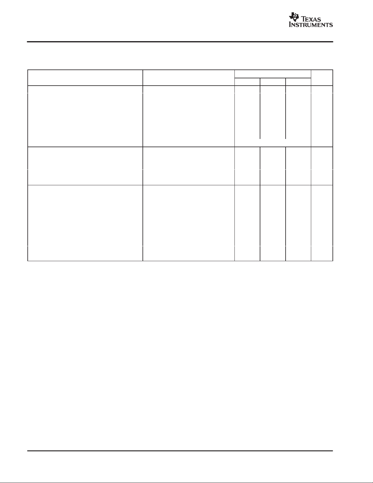
ELECTRICAL CHARACTERISTICS: VS = 2.7V to 5.5V (continued)
Boldface limits apply over the temperature range, TA = −40°C to +85°C. VS = 5V.
All specifications at TA = +25°C, RL = 1kΩ connected to VS/2 and V
PARAMETER UNITMAXTYP
OUTPUT
Voltage Output Swing from Rail
TA = −40°C to +85°C RL = 10kW, AOL 100dB 50 mV
TA = −40°C to +85°C RL = 1kW, AOL 100dB 200 mV
Output Current I
Short-Circuit Current I
Capacitive Load Drive C
POWER SUPPLY
Operating Voltage Range V
Minimum Operating Voltage 2.5 V
Quiescent Current (per amplifier) I
TA = −40°C to +85°C IO = 0 8.5 mA
TEMPERATURE RANGE
Specified Range −40 +85 °C
Operating Range −55 +150 °C
Storage Range −55 +150 °C
Thermal Resistance q
MSOP-8 Surface Mount 150 °C/W
SO-8 Surface Mount 150 °C/W
DIP-8 100 °C/W
SO-14 Surface Mount 100 °C/W
SSOP-16 Surface Mount 100 °C/W
(1)
VS = +5V .
(2)
V
= 0.25V to 2.75V .
OUT
(3)
NTSC signal generator used. See Figure 6 for test circuit.
(4)
Output voltage swings are measured between the output and power supply rails.
(5)
See typical characteristic curve, Output Voltage Swing vs Output Current.
(4)
V
OUT
OUT
SC
LOAD
JA
RL = 10kΩ, AOL ≥ 100dB 10 50 mV
RL = 1kΩ, AOL ≥ 100dB 25 200 mV
S
Q
= VS/2, unless otherwise noted.
OUT
OPA350, OPA2350, OPA4350
MINTEST CONDITIONS
See Typical Characteristics
TA = −40°C to +85°C 2.7 5.5 V
IO = 0 5.2 7.5 mA
(1)
(5)
±40
±80 mA
www.ti.com
mA
4
www.ti.com
THD+N (%)
Harmonic Distortion (%)
SBOS099C − SEPTEMBER 2000 − REVISED JANUARY 2005
TYPICAL CHARACTERISTICS
All specifications at TA = +25°C, VS = +5V , and RL = 1kΩ connected to VS/2, unless otherwise noted.
POWER SUPPLY ANDCOMMON−MODE
160
140
120
100
80
60
Voltage Gain (dB)
40
20
0
OPEN-LOOP GAIN/PHASE vs FREQUENCY
0.1 1
φ
G
10 100 1k 10k 100k 1M 10M 100M
Frequency (Hz)
0
45
−
)
_
90
−
Phase (
135
−
180
−
100
90
80
70
60
50
40
30
PSRR,CMRR (dB)
20
10
0
10 100 1k 10k 100k 1M 10M
REJECTION RATIOvs FREQUENCY
CMRR
(V
S
=−0.1V to 5.1V)
V
CM
Frequency(Hz)
"#$
%"#$
&"#$
PSRR
=+5V
INPUT VOLTAGE AND CURRENT NOISE
100k
10k
1k
100
VoltageNoise (nV√Hz)
10
1
10 100 1k 10k 100k 1M 10M
1
0.1
0.01
0.001
0.0001
SPECTRAL DENSITY vs FREQUENCY
Current Noise
Voltage Noise
Frequency (Hz)
TOTAL HARMONIC DISTORTION + NOISE
G = 100, 3VPP(VO=1Vto4V)
G=10,3VPP(VO=1Vto4V)
G = 1, 3VPP(VO=1Vto4V)
Input goes through transition region
G = 1, 2.5VPP(VO= 0.25Vto 2.75V)
Input does NOT go through transition region
10 100 1k 10k 100k
vs FREQUENCY
Frequency (Hz)
RL= 600Ω
10k
1k
100
10
1
0.1
140
130
120
110
100
90
Current Noise (fA√Hz)
80
Channel Separation (dB)
70
60
(−40dBc)
0.1
(−60dBc)
0.01
(−80dBc)
0.001
(−100dBc)
0.0001
(−120dBc)
CHANNEL SEPARATION vs FREQUENCY
Dual and quad devices.
10010 1k 1M100k10k 10M
Frequency (Hz)
HARMON ICDISTORTION + NOISE vs FREQUEN CY
1
G=1
VO=2.5V
PP
RL= 600Ω
3rd−Harmonic
1k 10k 100k 1M
2nd− Harmonic
Frequency (Hz)
5
"#$
0
%"#$
&"#$
SBOS099C − SEPTEMBER 2000 − REVISED JANUARY 2005
TYPICAL CHARACTERISTICS (continued)
All specifications at TA = +25°C, VS = +5V , and RL = 1kΩ connected to VS/2, unless otherwise noted.
www.ti.com
DIFFERENTIAL GAIN/PHASE vs RESISTIVE LOAD
0.5
0.4
)
_
0.3
0.2
Differential Gain (%)
Differential Phase (
0.1
0
0 100 200 300 500400 600 800700 900 100
COMMON−MODEAND POWER−SUPPLY REJECTION RATIO
100
90
80
CMRR (dB)
70
60
−75 −50 −25 0 2 5 50 75 100 125
Phase
Gain
Resistive Load (Ω)
vs TEMP ERATUR E
CMRR, VS=5.5V
(VCM=−0.1V to +5.6V)
CMRR, VS=2.7V
(V
CM
PSRR
Temperature (_C)
G=2
=1.4V
V
O
NTSC Signal Generator
SeeFigure6fortestcircuit.
= −0.1Vto +2.8V)
110
100
90
80
70
130
125
120
115
Open−Loop Gain (dB)
110
−
75−50−250255075100125
40
35
30
s)
µ
25
20
PSRR(dB)
15
Slew Rate (V/
10
5
0
−75−50−
OPEN−LOOP GAIN vs TEMPERATURE
Ω
RL=1k
Ω
RL=10k
Ω
RL=600
Temperature (_C)
SLEW RATE vs TEMPERATURE
Negative Slew Rate
Positive Slew Rate
250 255075100125
Temperature (_C)
Quiescent Current (mA)
6
QUIESCENT CURRENT AND
SHORT−CIRCUIT CURRENT vs TEMPERATURE
7.0
6.5
6.0
5.5
5.0
4.5
4.0
3.5
−75−50−
25 0 25 50 75 100 125
Temperature (_C)
+I
I
−
SC
I
Q
QUIESCENT CURRENT vs SUPPLY VOLTAGE
SC
100
90
80
70
60
50
Short−C ircuitCurrent (mA)
40
30
6.0
Per Amplifier
5.5
5.0
4.5
4.0
QuiescentCurrent (mA)
3.5
3.0
2.0 2.5 3.0 3.5 4.0 4.5 5.0 5.5
Supply Voltage (V)
www.ti.com
M
0
SBOS099C − SEPTEMBER 2000 − REVISED JANUARY 2005
TYPICAL CHARACTERISTICS (continued)
All specifications at TA = +25°C, VS = +5V , and RL = 1kΩ connected to VS/2, unless otherwise noted.
"#$
%"#$
&"#$
)
Ω
Output Impedance (
100
Input Bias Current (pA)
0.001
1k
10
1
0.1
100
10
0.1
0.01
INPUT BIAS CURRENT vs TEMPERATURE
−75−50−
CLOSED−LOOP OUTPUT IMPEDANCE vs FREQUENCY
1
25 0 25 50 75 100 125
Temperature (_C)
G = 100
G=10
G=1
INPUT BIAS CURRENT
1.5
1.0
0.5
0.0
Input Bias Current (pA)
−
0.5
−0.5 0.0 0.5 1.0 2.01.5 2.5 3.0 3.5 4.0 5.04.5 5.5
6
5
)
PP
4
3
2
Output Voltage (V
1
vs INPUT COMMON−MODE VOLTAGE
Common−Mode Voltage (V)
MAXIMUM OUTPUT VOLTAGE vs FREQUENCY
VS=5.5V
VS=2.7V
Maximum output
voltage without
slewrate−induced
distortion.
0.0001
1 10 100 1k 10k 100k 1M 10M 100
Frequency (Hz)
OUTPUT VOLTAGE SWING vs OUTPUT CURRENT
V+
(V+)−1
(V+)−2
(V−)+2
Output Voltage (V)
(V−)+1
(V−)
+125_C
Depending on circuit configuration
(including closed−loop gain) performance
may be degraded in shaded region.
+125_C
0
±
10
Output Current (mA)
−55_
+25_C
±
20
0
100k
Frequency (Hz)
OPEN−LOOPGAIN vs OUTPUT VOLTAGE SWING
140
I
=250µA
OUT
130
+25_C
C
−55_
C
±
30
±
4
120
110
100
90
80
Open−Loop Gain (dB)
70
60
0204060 10080 120 160140 180 200
Output Voltage Swing from Rails (mV)
I
I
OUT
=2.5mA
OUT
=4.2mA
100M1M 10M
7
"#$
%"#$
&"#$
SBOS099C − SEPTEMBER 2000 − REVISED JANUARY 2005
TYPICAL CHARACTERISTICS (continued)
All specifications at TA = +25°C, VS = +5V , and RL = 1kΩ connected to VS/2, unless otherwise noted.
www.ti.com
OFFSET VOLTAGE
18
16
14
12
10
8
6
4
Perce n tof Amplifiers (%)
2
0
−500
SMALL−SIGNAL OVERSHOOT vs LOAD CAPACITANCE
80
70
60
50
40
30
Overshoot (%)
20
10
0
10
PRODUC TIONDISTRIBUTION
450−400−350
−
250−200−150−100
−300
−
Offset Voltage (µV)
G=1
G=−1
Load Capacitance (pF)
0
50
−
G=±10
50
Typ ic a ldistributionof
packaged units.
100
150
200
250
300
350
400
450
500
1M100 1k 10k 100k
OFFSET VOLTAGE DRIFT
20
18
16
14
12
10
8
6
Percent of Amplifiers (%)
4
2
0
0123456789101112131415
10
s)
µ
1
Settling Time (
0.1
−
1
PRODUCTION DISTRIBUTION
Typicalproduction
distributi on of
packagedunits.
Offset VoltageDrift (µV/_ C)
SETTLING TIME vs CLOSED−LOOP GAIN
0.01%
0.1%
−
10
Closed−Loop Gain (V/V)
−
100
SMALL−SIGNALSTEP RESPONSE
50mV/div
= 100pF
C
L
100ns/div
1V/div
LARGE−SIGNALSTEP RESPONSE
= 100pF
C
L
200ns/div
8
 Loading...