

Burr Brown OPA2338EA-3K, OPA2338UA, OPA337EA-250, OPA337UA, OPA338UA Datasheet
...
1
®
OPA337, OPA2337
OPA338, OPA2338
®
International Airport Industrial Park • Mailing Address: PO Box 11400, Tucson, AZ 85734 • Street Address: 6730 S. Tucson Blvd., Tucson, AZ 85706 • Tel: (520) 746-1111
Twx: 910-952-1111 • Internet: http://www.burr-brown.com/ • Cable: BBRCORP • Telex: 066-6491 • FAX: (520) 889-1510 • Immediate Product Info: (800) 548-6132
PDS-1410C
© 1997 Burr-Brown Corporation PDS-1410D Printed in U.S.A. June, 2000
FEATURES
●
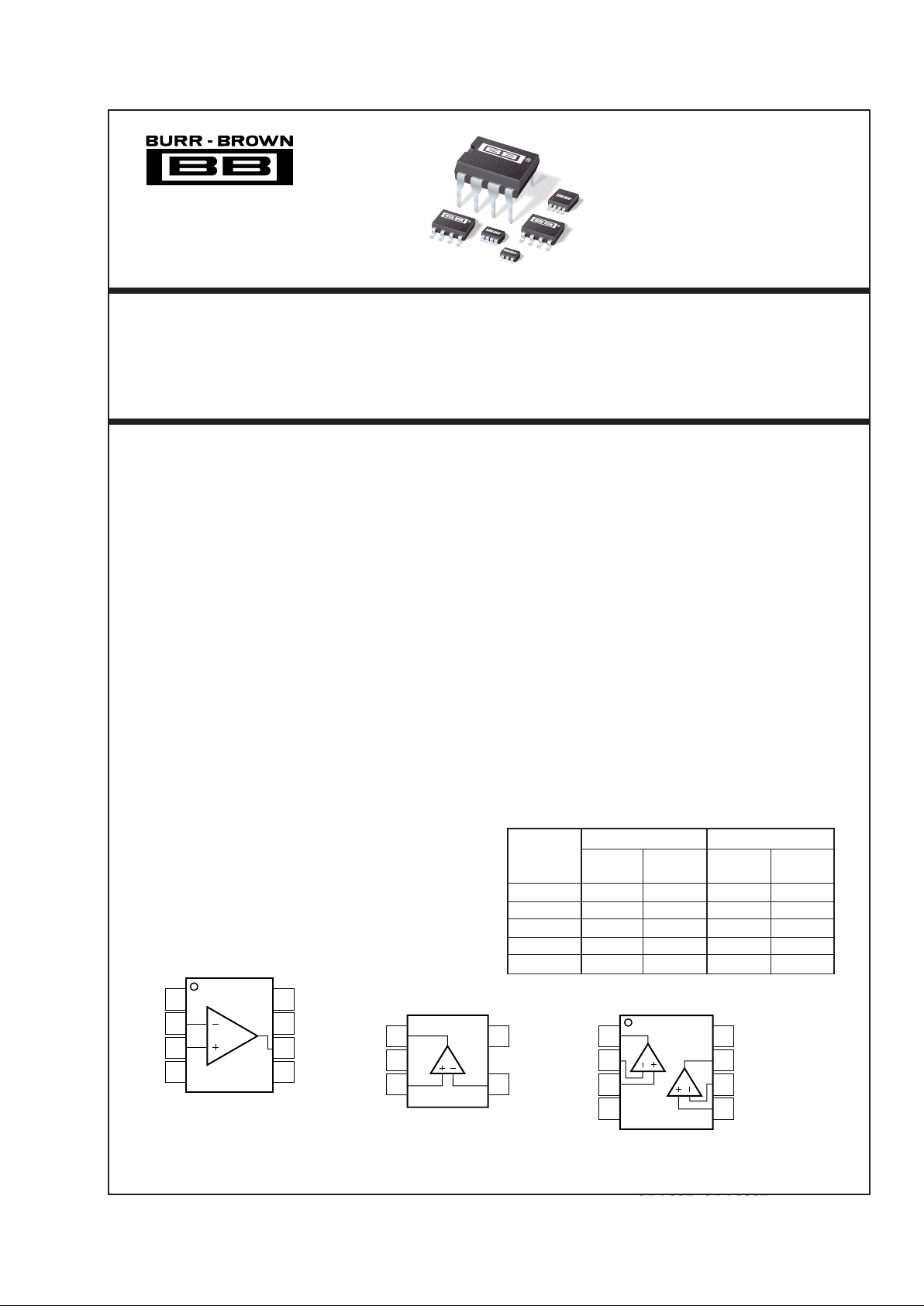
Micro
SIZE PACKAGES:
SOT23-5
SOT23-8
● SINGLE-SUPPLY OPERATION
● RAIL-TO-RAIL OUTPUT SWING
● FET-INPUT: IB = 10pA max
● HIGH SPEED:
OPA337: 3MHz, 1.2V/µs (G = 1)
OPA338: 12.5MHz, 4.6V/µs (G = 5)
● OPERATION FROM 2.5V to 5.5V
● HIGH OPEN-LOOP GAIN: 120dB
● LOW QUIESCENT CURRENT: 525µA/amp
● SINGLE AND DUAL VERSIONS
DESCRIPTION
The OPA337 and OPA338 series rail-to-rail output CMOS
operational amplifiers are designed for low cost and miniature applications. Packaged in the new SOT23-8, the
OPA2337EA and OPA2338EA are Burr-Brown’s smallest
dual op amps. At 1/4 the size of a conventional SO-8 surface
mount, they are ideal for space-sensitive applications.
Utilizing advanced CMOS technology, OPA337 and
OPA338 op amps provide low bias current, high-speed
operation, high open-loop gain, and rail-to-rail output
swing. They operate on a single supply with operation as
low as 2.5V while drawing only 525µA quiescent current.
In addition, the input common-mode voltage range includes ground—ideal for single-supply operation.
The OPA337 series is unity-gain stable. The OPA338
series is optimized for gains greater than or equal to five.
They are easy to use and free from phase inversion and
overload problems found in some other op amps. Excellent performance is maintained as the amplifiers swing to
their specified limits. The dual versions feature completely
independent circuitry for lowest crosstalk and freedom
from interaction, even when overdriven or overloaded.
Micro
SIZE, Single-Supply
CMOS OPERATIONAL AMPLIFIERS
Micro
Amplifier
™
Series
APPLICATIONS
● BATTERY-POWERED INSTRUMENTS
● PHOTODIODE PRE-AMPS
● MEDICAL INSTRUMENTS
● TEST EQUIPMENT
● AUDIO SYSTEMS
● DRIVING ADCs
● CONSUMER PRODUCTS
1
2
3
4
8
7
6
5
V+
Out B
–In B
+In B
Out A
–In A
+In A
V–
OPA2337, OPA2338
8-Pin DIP
(1)
, SO-8, SOT23-8
A
B
1
2
3
4
8
7
6
5
NC
V+
Output
NC
NC
–In
+In
V–
OPA337, OPA338
8-Pin DIP
(1)
, SO-8, MSOP-8
(1)
1
2
3
5
4
V+
–In
Out
V–
+In
OPA337, OPA338
SOT23-5
NOTE: (1) DIP AND MSOP-8 versions for OPA337, OPA2337 only.
SPICE Model available at www.burr-brown.com
For most current data sheet and other product
information, visit www.burr-brown.com
OPA337
OPA2337
OPA338
OPA2338
G = 1 STABLE G ≥ 5 STABLE
SINGLE DUAL SINGLE DUAL
PACKAGE OPA337 OPA2337 OPA338 OPA2338
SOT23-5 ✔✔
SOT23-8 ✔✔
MSOP-8 ✔
SO-8 ✔✔ ✔✔
DIP-8 ✔✔
OPA337
OPA2337
OPA2338
2
®
OPA337, OPA2337
OPA338, OPA2338
SPECIFICATIONS: VS = 2.7V to 5.5V
At TA = +25°C, and RL = 25kΩ connected to VS/2, unless otherwise noted.
Boldface limits apply over the specified temperature range, –40°C to +85°C, V
S
= 5V.
The information provided herein is believed to be reliable; however, BURR-BROWN assumes no responsibility for inaccuracies or omissions. BURR-BROWN assumes
no responsibility for the use of this information, and all use of such information shall be entirely at the user’s own risk. Prices and specifications are subject to change
without notice. No patent rights or licenses to any of the circuits described herein are implied or granted to any third party. BURR-BROWN does not authorize or warrant
any BURR-BROWN product for use in life support devices and/or systems.
OPA337NA, EA, UA, PA
OPA2337EA, UA, PA
OPA338NA, UA
OPA2338EA, UA
PARAMETER CONDITION MIN TYP
(1)
MAX UNITS
OFFSET VOLTAGE
Input Offset Voltage V
OS
±0.5 ±3mV
T
A
= –40°C to +85°C ±3.5 mV
vs Temperature dV
OS
/dT ±2 µV/°C
vs Power Supply Rejection Ratio PSRR V
S
= 2.7V to 5.5V 25 125 µV/V
T
A
= –40°C to +85°C VS = 2.7V to 5.5V 125 µV/V
Channel Separation (dual versions) dc 0.3 µV/V
INPUT BIAS CURRENT
Input Bias Current I
B
±0.2 ±10 pA
T
A
= –40°C to +85°C See Typical Curve
Input Offset Current I
OS
±0.2 ±10 pA
NOISE
Input Voltage Noise, f = 0.1Hz to 10Hz 6 µVp-p
Input Voltage Noise Density, f = 1kHz e
n
26 nV/√Hz
Current Noise Density, f = 1kHz i
n
0.6 fA/√Hz
INPUT VOLTAGE RANGE
Common-Mode Voltage Range V
CM
TA = –40°C to +85°C –0.2 (V+) – 1.2 V
Common-Mode Rejection Ratio CMRR –0.2V < V
CM
< (V+) – 1.2V 74 90 dB
T
A
= –40°C to +85°C –0.2V < V
CM
< (V+) – 1.2V 74 dB
INPUT IMPEDANCE
Differential 10
13
|| 2 Ω || pF
Common-Mode 10
13
|| 4 Ω || pF
OPEN-LOOP GAIN
Open-Loop Voltage Gain A
OLRL
= 25kΩ, 125mV < VO < (V+) – 125mV 100 120 dB
T
A
= –40°C to +85°C RL = 25kΩ, 125mV < VO < (V+) – 125mV 100 dB
R
L
= 5kΩ, 500mV < VO < (V+) – 500mV 100 114 dB
T
A
= –40°C to +85°C RL = 5kΩ, 500mV < VO < (V+) – 500mV 100 dB
OPA337 FREQUENCY RESPONSE
Gain-Bandwidth Product GBW V
S
= 5V, G = 1 3 MHz
Slew Rate SR V
S
= 5V, G = 1 1.2 V/µs
Settling Time: 0.1% V
S
= 5V, 2V Step, CL = 100pF, G = 1 2 µs
0.01% V
S
= 5V, 2V Step, CL = 100pF, G = 1 2.5 µs
Overload Recovery Time V
IN
• G = V
S
2 µs
Total Harmonic Distortion + Noise THD+N V
S
= 5V, VO = 3Vp-p, G = 1, f = 1kHz 0.001 %
OPA338 FREQUENCY RESPONSE
Gain-Bandwidth Product GBW V
S
= 5V, G = 5 12.5 MHz
Slew Rate SR V
S
= 5V, G = 5 4.6 V/µs
Settling Time: 0.1% V
S
= 5V, 2V Step, CL = 100pF, G = 5 1.4 µs
0.01% V
S
= 5V, 2V Step, CL = 100pF, G = 5 1.9 µs
Overload Recovery Time V
IN
• G = V
S
0.5 µs
Total Harmonic Distortion + Noise THD+N V
S
= 5V, VO = 3Vp-p, G = 5, f = 1kHz 0.0035 %
OUTPUT
Voltage Output Swing from Rail
(2)
RL = 25kΩ, AOL ≥ 100dB 40 125 mV
T
A
= –40°C to +85°C RL = 25kΩ, AOL ≥ 100dB 125 mV
R
L
= 5kΩ, AOL ≥ 100dB 150 500 mV
T
A
= –40°C to +85°C RL = 5kΩ, AOL ≥ 100dB 500 mV
Short-Circuit Current I
SC
±9mA
Capacitive Load Drive C
LOAD
See Typical Curve
POWER SUPPLY
Specified Voltage Range V
S
TA = –40°C to +85°C 2.7 5.5 V
Minimum Operating Voltage 2.5 V
Quiescent Current (per amplifier) I
Q
IO = 0 0.525 1 mA
T
A
= –40°C to +85°C IO = 0 1.2 mA
3
®
OPA337, OPA2337
OPA338, OPA2338
PACKAGE SPECIFIED
DRAWING TEMPERATURE PACKAGE ORDERING TRANSPORT
PRODUCT DESCRIPTION PACKAGE NUMBER RANGE MARKING NUMBER
(1)
MEDIA
OPA337 Series
OPA337NA Single, G = 1 Stable 5-Lead SOT23-5 331 –40 °C to +85°C C37 OPA337NA/250 Tape and Reel
"" """"OPA337NA/3K Tape and Reel
OPA337EA Single, G = 1 Stable MSOP-8 337 –40 °C to +85°C G37 OPA337EA/250 Tape and Reel
"" """"OPA337EA/2K5 Tape and Reel
OPA337PA Single, G = 1 Stable 8-Pin DIP 006 –40°C to +85°C OPA337PA OPA337PA Rails
OPA337UA Single, G = 1 Stable SO-8 Surface Mount 182 –40°C to +85°C OPA337UA OPA337UA Rails
"" """"OPA337UA/2K5 Tape and Reel
OPA2337EA Dual, G = 1 Stable 8-Lead SOT23-8 348 –40°C to +85°C A7 OPA2337EA/250 Tape and Reel
"" """"OPA2337EA/3K Tape and Reel
OPA2337PA Dual, G = 1 Stable 8-Pin DIP 006 –40°C to +85°C OPA2337PA OPA2337PA Rails
OPA2337UA Dual, G = 1 Stable SO-8 Surface Mount 182 –40°C to +85°C OPA2337UA OPA2337UA Rails
"" """"OPA2337UA/2K5 Tape and Reel
OPA338 Series
OPA338NA Single, G ≥ 5 Stable 5-Lead SOT23-5 331 –40°C to +85°C A38 OPA338NA/250 Tape and Reel
"" """"OPA338NA/3K Tape and Reel
OPA338UA Single, G
≥ 5 Stable SO-8 Surface Mount 182 –40°C to +85°C OPA338UA OPA338UA Rails
"" """"OPA338UA/2K5 Tape and Reel
OPA2338EA Dual, G
≥ 5 Stable 8-Lead SOT23-8 348 –40°C to +85°C A8 OPA2338EA/250 Tape and Reel
"" """"OPA2338EA/3K Tape and Reel
OPA2338UA Dual, G
≥ 5 Stable SO-8 Surface Mount 182 –40°C to +85°C OPA2338UA OPA2338UA Rails
"" """"OPA2338UA/2K5 Tape and Reel
NOTES: (1) Models with a slash (/) are available only in Tape and Reel in the quantities indicated (e.g., /2K5 indicates 2500 devices per reel). Ordering 2500 pieces
of “OPA2337UA/2K5” will get a single 2500-piece Tape and Reel.
SPECIFICATIONS: VS = 2.7V to 5.5V (Cont.)
At TA = +25°C, and RL = 25kΩ connected to VS/2, unless otherwise noted.
Boldface limits apply over the specified temperature range, –40°C to +85°C, V
S
= 5V.
OPA337NA, EA, UA, PA
OPA2337EA, UA, PA
OPA338NA, UA
OPA2338EA, UA
PARAMETER CONDITION MIN TYP MAX UNITS
TEMPERATURE RANGE
Specified Range –40 +85 °C
Operating Range –55 +125 °C
Storage Range –55 +125 °C
Thermal Resistance
θ
JA
SOT23-5 Surface Mount 200 °C/W
SOT23-8 Surface Mount 200 °C/W
MSOP-8 150 °C/W
SO-8 Surface Mount 150 °C/W
8-Pin DIP 100 °C/W
NOTES: (1) V
S
= 5V. (2) Output voltage swings are measured between the output and negative and positive power supply rails.
ELECTROSTATIC
DISCHARGE SENSITIVITY
This integrated circuit can be damaged by ESD. Burr-Brown
recommends that all integrated circuits be handled with
appropriate precautions. Failure to observe proper handling
and installation procedures can cause damage.
ESD damage can range from subtle performance degradation to complete device failure. Precision integrated circuits
may be more susceptible to damage because very small
parametric changes could cause the device not to meet its
published specifications.
Supply Voltage ................................................................................... 5.5V
Input Voltage
(2)
.................................................. (V–) –0.5V to (V+) +0.5V
Input Current
(2)
................................................................................. 10mA
Output Short Circuit
(3)
.............................................................. Continuous
Operating Temperature .................................................. –55 °C to +125°C
Storage Temperature ..................................................... –55°C to +125°C
Junction Temperature ...................................................................... 150°C
Lead Temperature (soldering, 10s) ................................................. 300°C
NOTES: (1) Stresses above these ratings may cause permanent damage.
Exposure to absolute maximum ratings for extended periods may degrade
device reliability. (2) Input signal voltage is limited by internal diodes
connected to power supplies. See text. (3) Short circuit to ground, one
amplifier per package.
ABSOLUTE MAXIMUM RATINGS
(1)
PACKAGE/ORDERING INFORMATION
 Loading...