

Burr Brown OPA37GU, OPA37GU-2K5, OPA27GU-2K5, OPA27GU, OPA27GP Datasheet
...
®
OPA27
OPA27
Ultra-Low Noise Precision
OPERATIONAL AMPLIFIERS
OPA27
OPA37
FEATURES
● LOW NOISE: 4.5nV/√Hz max at 1kHz
● LOW OFFSET: 100
● LOW DRIFT: 0.4
µV max
µV/°C
● HIGH OPEN-LOOP GAIN: 117dB min
● HIGH COMMON-MODE REJECTION:
100dB min
● HIGH POWER SUPPLY REJECTION:
94dB min
● FITS OP-07, OP-05, AD510, AD517
SOCKETS
DESCRIPTION
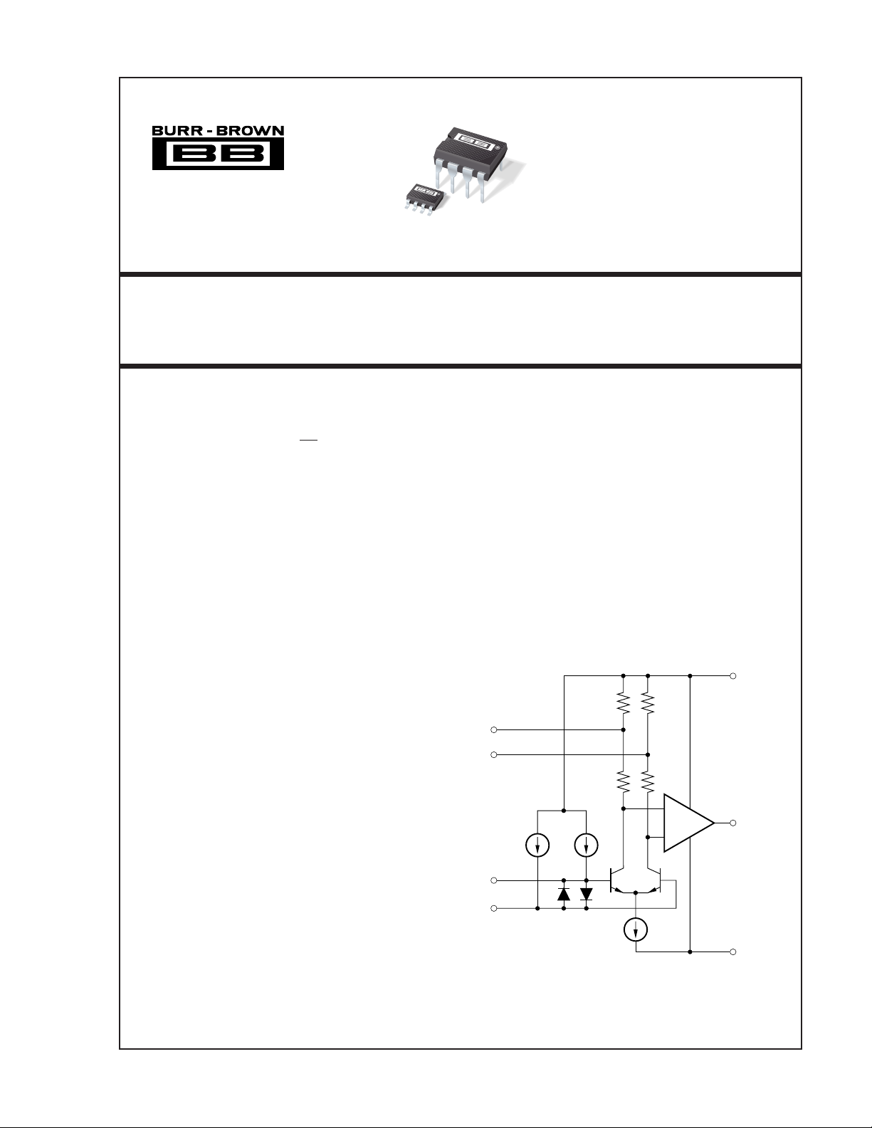
The OPA27/37 is an ultra-low noise, high precision
monolithic operational amplifier.
Laser-trimmed thin-film resistors provide excellent
long-term voltage offset stability and allow superior
voltage offset compared to common zener-zap techniques.
A unique bias current cancellation circuit allows bias
and offset current specifications to be met over the full
–55°C to +125°C temperature range.
The OPA27 is internally compensated for unity-gain
stability. The decompensated OPA37 requires a closedloop gain ≥ 5.
The Burr-Brown OPA27/37 is an improved replacement for the industry-standard OP-27/OP-37.
APPLICATIONS
● PRECISION INSTRUMENTATION
● DATA ACQUISITION
● TEST EQUIPMENT
● PROFESSIONAL AUDIO EQUIPMENT
● TRANSDUCER AMPLIFIER
● RADIATION HARD EQUIPMENT
8
Trim
1
Trim
2
–In
3
+In
7
6
4
+V
CC
Output
–V
CC
International Airport Industrial Park • Mailing Address: PO Box 11400, Tucson, AZ 85734 • Street Address: 6730 S. Tucson Blvd., Tucson, AZ 85706 • Tel: (520) 746-1111 • Twx: 910-952-1111
Internet: http://www.burr-brown.com/ • FAXLine: (800) 548-6133 (US/Canada Only) • Cable: BBRCORP • Telex: 066-6491 • FAX: (520) 889-1510 • Immediate Product Info: (800) 548-6132
®
© 1984 Burr-Brown Corporation PDS-466M Printed in U.S.A. March, 1998
1
OPA27, 37
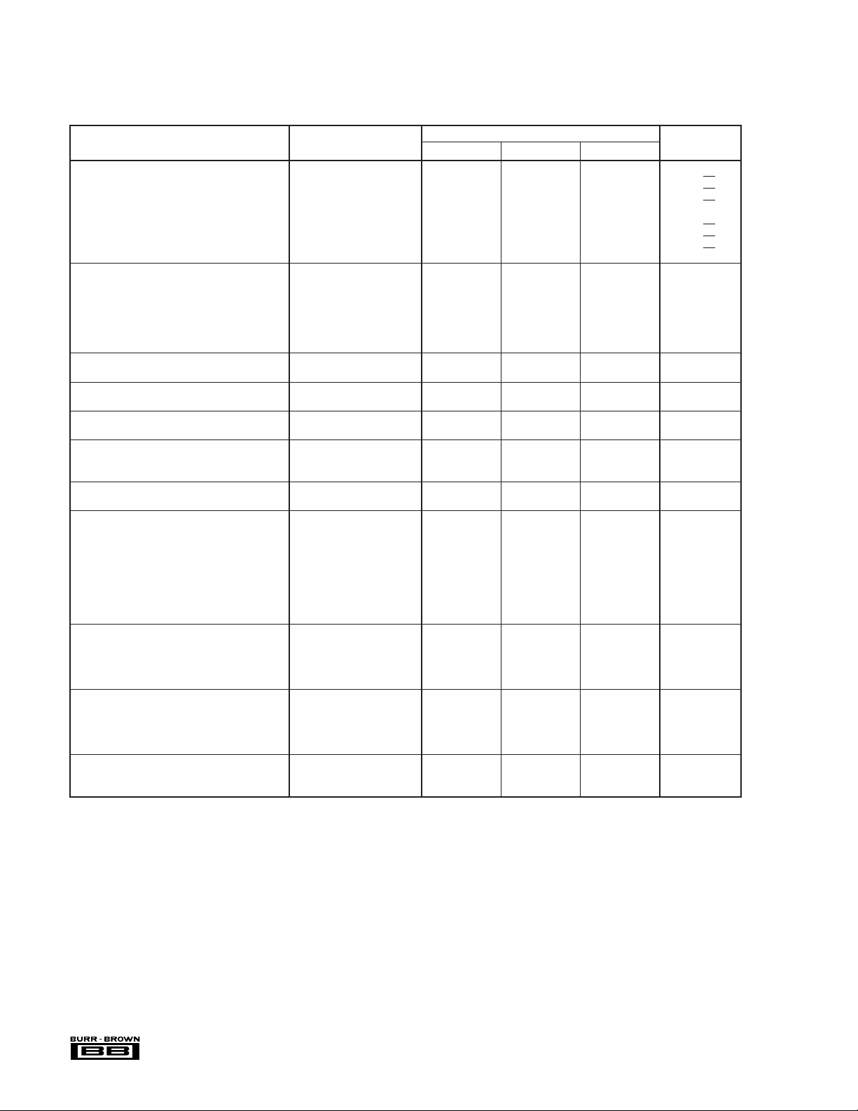
SPECIFICATIONS
At V
= ±15V and TA = +25°C, unless otherwise noted.
CC
OPA27/37G
PARAMETER CONDITIONS MIN TYP MAX UNITS
INPUT NOISE
Voltage, fO = 10Hz 3.8 8.0 nV/√Hz
Current,
OFFSET VOLTAGE
Input Offset Voltage ±25 ±100 µV
Average Drift
Long Term Stability
(6)
f
= 30Hz 3.3 5.6 nV/√Hz
O
f
= 1kHz 3.2 4.5 nV/√Hz
O
f
= 0.1Hz to 10Hz 0.09 0.25 µVp-p
B
(1)
fO = 10Hz 1.7 pA/√Hz
f
= 30Hz 1.0 pA/√Hz
O
f
= 1kHz 0.4 0.6 pA/√Hz
O
(2)
(3)
(4)
T
A MIN
to T
A MAX
±0.4 ±1.8
0.4 2.0 µV/mo
(6)
µV/°C
Supply Rejection ±V
= 4 to 18V 94 120 dB
CC
±V
= 4 to 18V ±1 ±20 µV/V
CC
BIAS CURRENT
Input Bias Current ±15 ±80 nA
OFFSET CURRENT
Input Offset Current 10 75 nA
IMPEDANCE
Common-Mode 2 || 2.5 GΩ || pF
VOLTAGE RANGE
Common-Mode Input Range ±11 ±12.3 V
Common-Mode Rejection V
OPEN-LOOP VOLTAGE GAIN, DC R
FREQUENCY RESPONSE
Gain-Bandwidth Product
Slew Rate
(5)
(5)
= ±11VDC 100 122 dB
IN
≥ 2kΩ 117 124 dB
L
R
≥ 1kΩ 124 dB
L
OPA27 5
OPA37 45
(6)
(6)
8 MHz
63 MHz
VO = ±10V,
R
= 2kΩ
L
OPA27, G = +1 1.7
OPA37, G = +5 11
(6)
(6)
1.9 V/µs
11.9 V/µs
Settling Time, 0.01% OPA27, G = +1 25 µs
OPA37, G = +5 25 µs
RATED OUTPUT
Voltage Output R
Output Resistance DC, Open Loop 70 Ω
Short Circuit Current R
≥ 2kΩ±12 ±13.8 V
L
R
≥ 600Ω±10 ±12.8 V
L
= 0Ω 25 60
L
(6)
mA
POWER SUPPLY
Rated Voltage ±15 VDC
Voltage Range,
Derated Performance ±4 ±22 VDC
Current, Quiescent I
= 0mADC 3.3 5.7 mA
O
TEMPERATURE RANGE
Specification –40 +85 °C
Operating –40 +85 °C
NOTES: (1) Measured with industry-standard noise test circuit (Figures 1 and 2). Due to errors introduced by this method, these current noise specifications should
be used for comparison purposes only. (2) Offset voltage specification are measured with automatic test equipment after approximately 0.5 seconds from power turnon. (3) Unnulled or nulled with 8kΩ to 20kΩ potentiometer. (4) Long-term voltage offset vs time trend line does not include warm-up drift. (5) Typical specification only
on plastic package units. Slew rate varies on all units due to differing test methods. Minimum specification applies to open-loop test. (6) This parameter guaranteed by
design.
®
OPA27, 37
2
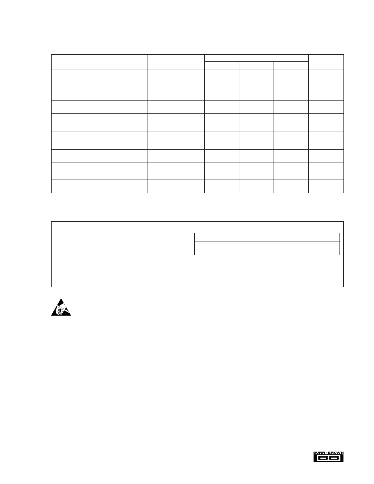
SPECIFICATIONS
At V
= ±15V and TA = +25°C, unless otherwise noted.
CC
OPA27/37G
PARAMETER CONDITIONS MIN TYP MAX UNITS
INPUT VOLTAGE
Input Offset Voltage ±48 ±220
Average Drift
Supply Rejection ±V
BIAS CURRENT
Input Bias Current ±21 ±150
OFFSET CURRENT
Input Offset Current
E, F, G 20 135
VOLTAGE RANGE
Common-Mode Input Range ±10.5
Common-Mode Rejection V
OPEN-LOOP GAIN, DC
Open-Loop Voltage Gain R
RATED OUTPUT
Voltage Output R
Short Circuit Current V
TEMPERATURE RANGE
Specification –40 +85 °C
NOTES: (1) Offset voltage specification are measured with automatic test equipment after approximately 0.5s from power turn-on. (2) Unnulled or nulled with 8kΩ to
20kΩ potentiometer. (3) This parameter guaranteed by design.
(1)
(2)
T
to T
A MIN
A MAX
= 4.5 to 18V
CC
±V
= 4.5 to 18V 90
CC
= ±11VDC 96
IN
≥ 2kΩ 113
L
= 2kΩ±11.0
L
= 0VDC 25 mA
O
(3)
(3)
(3)
(3)
(3)
±0.4 ±1.8
122 dB
±11.8 V
122 dB
120 dB
±13.4 V
(3)
(3)
(3)
(3)
µV
µV/°C
nA
nA
ABSOLUTE MAXIMUM RATINGS
Supply Voltage ................................................................................... ±22V
Internal Power Dissipation
Input Voltage ...................................................................................... ±V
Output Short-Circuit Duration
Differential Input Voltage
Differential Input Current
Storage Temperature Range ..........................................–55°C to +125°C
Operating Temperature Range.........................................–40°C to +85°C
Lead Temperature:
P (soldering, 10s) ....................................................................... +300°C
U (soldering, 3s) ......................................................................... +260°C
(1)
........................................................500mW
(2)
.................................................Indefinite
(3)
............................................................. ±0.7V
(3)
........................................................... ±25mA
CC
ELECTROSTATIC
DISCHARGE SENSITIVITY
This integrated circuit can be damaged by ESD. Burr-Brown
recommends that all integrated circuits be handled with
appropriate precautions. Failure to observe proper handling
and installation procedures can cause damage.
ESD damage can range from subtle performance degradation
to complete device failure. Precision integrated circuits may
be more susceptible to damage because very small parametric
changes could cause the device not to meet its published
specifications.
PACKAGE TYPE
8-Pin Plastic DIP (P) 100 °C/W
8-Pin SOIC (U) 160 °C/W
NOTES: (1) Maximum package power dissipation vs ambient temperature. (2) To
common with ±V
Current limiting resistors are not used in order to achieve low noise. If differential
input voltage exceeds ±0.7V, the input current should be limited to 25mA.
= 15V. (3) The inputs are protected by back-to-back diodes.
CC
θ
JA
UNITS
The information provided herein is believed to be reliable; however, BURR-BROWN assumes no responsibility for inaccuracies or omissions. BURR-BROWN assumes
no responsibility for the use of this information, and all use of such information shall be entirely at the user’s own risk. Prices and specifications are subject to change
without notice. No patent rights or licenses to any of the circuits described herein are implied or granted to any third party. BURR-BROWN does not authorize or warrant
any BURR-BROWN product for use in life support devices and/or systems.
3
OPA27, 37
®

CONNECTION DIAGRAMS
Top View P, U Packages
Offset Trim
–V
–In
+In
1
2
3
4
CC
10Ω
8
7
6
5
0.1µF
100kΩ
DUT
Voltage Gain
Total = 50,000
Offset Trim
+V
CC
Output
NC
2kΩ
4.7µF
PACKAGE/ORDERING INFORMATION
(1)
PRODUCT
OPA27GP Plastic –40 to +85 ±100 006
OPA27GU
NOTE: (1) Packages for OPA37 are same as for OPA27. (2) OPA27GU may
be marked OPA27U. Likewise, OPA37GU may be marked OPA37U. (3) For
detailed drawing and dimension table, please see end of data sheet, or
Appendix C of Burr-Brown IC Data Book.
OPA111
100kΩ
PACKAGE RANGE (°C) MAX (µV), 25°C NUMBER
(2)
SOIC –40 to +85 ±100 182
4.3kΩ
TEMPERATURE VOLTAGE DRAWING
22µF
2.2µF
OFFSET PACKAGE
Scope
x1
= 1MΩ
R
IN
(3)
NOTE: All capacitor values are for nonpolarized capacitors only.
FIGURE 1. 0.1Hz to 10Hz Noise Test Circuit.
0.1µF
24.3kΩ
0.1Hz TO 10Hz NOISE
1s/div 40nV/div
110kΩ
FIGURE 2. Low Frequency Noise.
®
OPA27, 37
4
 Loading...