

Burr Brown OPA2277U, OPA277PA, OPA277UA, OPA4277PA, OPA4277UA-2K5 Datasheet
...
®
For most current data sheet and other product
information, visit www.burr-brown.com
OPERATIONAL AMPLIFIERS
O
P
A
2
7
7
OPA277
O
P
A
2
27
7
OPA2277
O
PA
OPA4277
4277
High Precision
OPA277
OPA2277
OPA4277
FEATURES
● ULTRA LOW OFFSET VOLTAGE: 10µV
● ULTRA LOW DRIFT: ±0.1µV/°C
● HIGH OPEN-LOOP GAIN: 134dB
● HIGH COMMON-MODE REJECTION: 140dB
● HIGH POWER SUPPLY REJECTION: 130dB
● LOW BIAS CURRENT: 1nA max
● WIDE SUPPLY RANGE: ±2V to ±18V
● LOW QUIESCENT CURRENT: 800 µA/amp
● SINGLE, DUAL, AND QUAD VERSIONS
● REPLACES OP-07, OP-77, OP-177
DESCRIPTION
The OPA277 series precision op amps replace the industry
standard OP-177. They offer improved noise, wider output
voltage swing, and are twice as fast with half the quiescent
current. Features include ultra low offset voltage and drift, low
bias current, high common-mode rejection, and high power
supply rejection. Single, dual, and quad versions have identical
specifications for maximum design flexibility.
OPA277 series op amps operate from ±2V to ±18V supplies
with excellent performance. Unlike most op amps which
are specified at only one supply voltage, the OPA277 series
is specified for real-world applications; a single limit applies over the ±5V to ±15V supply range.
High performance
is maintained as the amplifiers swing to their specified limits.
APPLICATIONS
● TRANSDUCER AMPLIFIER
● BRIDGE AMPLIFIER
● TEMPERATURE MEASUREMENTS
● STRAIN GAGE AMPLIFIER
● PRECISION INTEGRATOR
● BATTERY POWERED INSTRUMENTS
● TEST EQUIPMENT
Because the initial offset voltage (±20µV max) is so low, user
adjustment is usually not required. However, the single version
(OPA277) provides external trim pins for special applications.
OPA277 op amps are easy to use and free from phase inversion
and overload problems found in some other op amps. They are
stable in unity gain and provide excellent dynamic behavior
over a wide range of load conditions. Dual and quad versions
feature completely independent circuitry for lowest crosstalk
and freedom from interaction, even when overdriven or overloaded.
Single (OPA277) and dual (OPA2277) versions are available
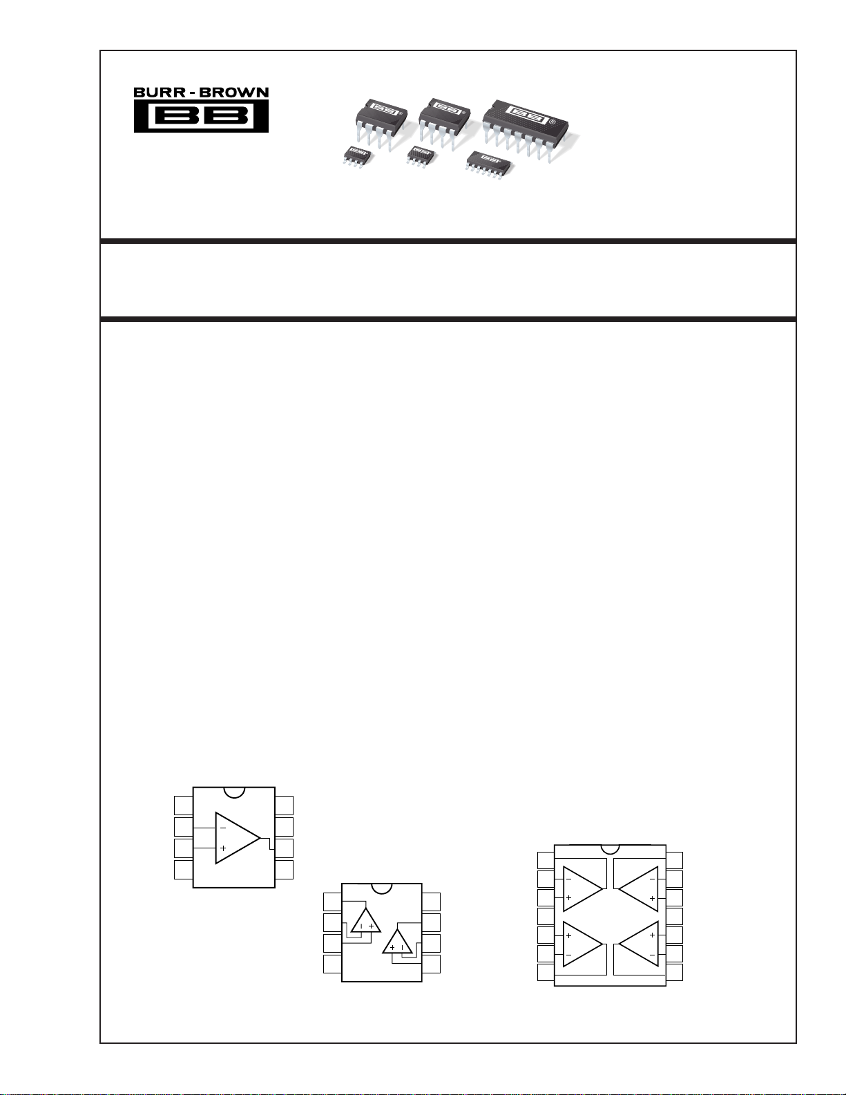
OPA277
Offset Trim
1
2
–In
3
+In
4
V–
8-Pin DIP, SO-8
IInternational Airport Industrial Park • Mailing Address: PO Box 11400, Tucson, AZ 85734 • Street Address: 6730 S. Tucson Blvd., Tucson, AZ 85706 • Tel: (520) 746-1111
Twx: 910-952-1111 • Internet: http://www.burr-brown.com/ • Cable: BBRCORP • Telex: 066-6491 • FAX: (520) 889-1510 • Immediate Product Info: (800) 548-6132
8
7
6
5
Out A
–In A
+In A
Offset Trim
V+
Output
NC
1
2
3
V–
4
OPA2277
A
B
8-Pin DIP, SO-8
in 8-pin DIP and SO-8 surface-mount packages. The quad
(OPA4277) comes in 14-pin DIP and SO-14 surface-mount
packages. All are fully specified from
–40°C to +85°C and
operate from –55°C to +125°C.
OPA4277
Out A
1
–In A
2
V+
8
Out B
7
–In B
6
+In B
5
+In A
V+
+In B
–In B
Out B
AD
3
4
5
BC
6
7
14-Pin DIP, SO-14
Out D
14
–In D
13
+In D
12
V–
11
+In C
10
–In C
9
Out C
8
© 1997 Burr-Brown Corporation PDS-1413D Printed in U.S.A. March, 1999

SPECIFICATIONS: VS = ±5V to VS = ±15V
At TA = +25°C, and RL = 2kΩ, unless otherwise noted.
Boldface limits apply over the specified temperature range, –40°C to +85°C.
OPA277P, U OPA2277PA, UA
OPA2277P, U OPA4277PA, UA
(1)
PARAMETER CONDITION MIN TYP
MAX MIN TYP
OFFSET VOLTAGE
Input Offset Voltage: V
OPA277P, U (high grade, single) ±10 ±20 µV
OS
OPA2277P, U (high grade, dual) ±10 ±25 µV
All PA, UA Versions ±20 ±50 µV
Input Offset Voltage Over Temperature
OPA277P, U (high grade, single) T
OPA2277P, U (high grade, dual) T
All PA, UA Versions T
Input Offset Voltage Drift dV
OPA277P, U (high grade, single) T
/dT
OS
OPA2277P, U (high grade, dual) T
All PA, UA Versions T
= –40°C to +85°C ±30 µV
A
= –40°C to +85°C ±50 µV
A
= –40°C to +85°C ±100 µV
A
= –40°C to +85°C ±0.1 ±0.15 µV/°C
A
= –40°C to +85°C ±0.1 ±0.25 µV/°C
A
= –40°C to +85°C ±0.15 ±1 µV/°C
A
Input Offset Voltage: (all models)
vs Time 0.2 ✻ µV/mo
vs Power Supply PSRR V
= –40°C to +85°C VS = ±2V to ±18V ±0.5 ±1 µV/V
T
A
Channel Separation (dual, quad) dc 0.1 ✻ µV/V
= ±2V to ±18V ±0.3 ±0.5 ✻ ±1 µV/V
S
INPUT BIAS CURRENT
Input Bias Current I
= –40°C to +85°C ±2 ±4 nA
T
A
Input Offset Current I
= –40°C to +85°C ±2 ±4 nA
T
A
B
OS
±0.5 ±1 ✻ ±2.8 nA
±0.5 ±1 ✻ ±2.8 nA
NOISE
Input Voltage Noise, f = 0.1 to 10Hz 0.22 ✻ µVp-p
0.035 ✻ µVrms
Input Voltage Noise Density, f = 10Hz e
f = 100Hz 8 ✻ nV/√Hz
n
12 ✻ nV/√Hz
f = 1kHz 8 ✻ nV/√Hz
f = 10kHz 8 ✻ nV/√Hz
Current Noise Density, f = 1kHz i
n
0.2 ✻ pA/√Hz
INPUT VOLTAGE RANGE
Common-Mode Voltage Range V
Common-Mode Rejection CMRR V
= –40°C to +85°C VCM = (V–) +2V to (V+) –2V 128 115 dB
T
A
CM
= (V–) +2V to (V+) –2V 130 140 115 ✻ dB
CM
(V–) +2 (V+) –2 ✻✻V
INPUT IMPEDANCE
Differential 100 || 3 ✻ MΩ || pF
Common-Mode V
= (V–) +2V to (V+) –2V 250 || 3 ✻ GΩ || pF
CM
OPEN-LOOP GAIN
Open-Loop Voltage Gain A
= –40°C to +85°C
T
A
= (V–)+0.5V to (V+)–1.2V, RL = 10kΩ
OLVO
VO = (V–)+0.5V to (V+)–1.5V, RL = 2kΩ
VO = (V–)+0.5V to (V+)–1.5V, RL = 2kΩ
126 134 ✻✻ dB
126 ✻ dB
140 ✻ dB
FREQUENCY RESPONSE
Gain-Bandwidth Product GBW 1 ✻ MHz
Slew Rate SR 0.8 ✻ V/µs
Settling Time, 0.1% V
0.01% V
Overload Recovery Time V
Total Harmonic Distortion + Noise THD+N 1kHz, G = 1, V
= ±15V, G = 1, 10V Step 14 ✻ µs
S
= ±15V, G = 1, 10V Step 16 ✻ µs
S
• G = V
IN
S
= 3.5Vrms 0.002 ✻ %
O
3 ✻ µs
OUTPUT
Voltage Output V
= –40°C to +85°C RL = 10kΩ (V–) +0.5 (V+) –1.2 ✻✻V
T
A
= –40°C to +85°C RL = 2kΩ (V–) +1.5 (V+) –1.5 ✻✻V
T
A
Short-Circuit Current I
Capacitive Load Drive C
O
SC
LOAD
RL = 10kΩ (V–) +0.5 (V+) –1.2 ✻✻V
= 2kΩ (V–) +1.5 (V+) –1.5 ✻✻V
R
L
±35 ✻ mA
See Typical Curve ✻
OPA277PA, UA
(1)
MAX UNITS
The information provided herein is believed to be reliable; however, BURR-BROWN assumes no responsibility for inaccuracies or omissions. BURR-BROWN assumes
no responsibility for the use of this information, and all use of such information shall be entirely at the user’s own risk. Prices and specifications are subject to change
without notice. No patent rights or licenses to any of the circuits described herein are implied or granted to any third party. BURR-BROWN does not authorize or warrant
any BURR-BROWN product for use in life support devices and/or systems.
®
OPA277, 2277, 4277
2

SPECIFICATIONS: VS = ±5V to VS = ±15V (CONT)
At TA = +25°C, and RL = 2kΩ, unless otherwise noted.
Boldface limits apply over the specified temperature range, –40°C to +85°C.
OPA277P, U OPA2277PA, UA
OPA2277P, U OPA4277PA, UA
(1)
PARAMETER CONDITION MIN TYP
MAX MIN TYP
OPA277PA, UA
(1)
MAX UNITS
POWER SUPPLY
Specified Voltage Range V
Operating Voltage Range ±2 ±18 ✻✻V
Quiescent Current (per amplifier) I
= –40°C to +85°C IO = 0 ±900 ✻ µA
T
A
TEMPERATURE RANGE
Specified Range –40 85 ✻✻°C
Operating Range –55 125 ✻✻°C
Storage Range –55 125 ✻✻°C
Thermal Resistance
SO-8 Surface-Mount 150 ✻ °C/W
8-Pin DIP 100 ✻ °C/W
14-Pin DIP 80 ✻ °C/W
SO-14 Surface-Mount 100 ✻ °C/W
✻ Specifications same as OPA277P, U.
NOTE: (1) V
= ±15V.
S
ABSOLUTE MAXIMUM RATINGS
Supply Voltage .................................................................................... 36V
Input Voltage ..................................................... (V–) –0.7V to (V+) +0.7V
Output Short-Circuit
Operating Temperature .................................................. –55°C to +125°C
Storage Temperature ..................................................... –55°C to +125°C
Junction Temperature ...................................................................... 150°C
Lead Temperature (soldering, 10s) ................................................. 300°C
NOTE: (1) Stresses above these rating may cause permanent damage.
Exposure to absolute maximum conditions for extended periods may degrade
device reliability. (2) Short-circuit to ground, one amplifier per package.
(2)
.............................................................. Continuous
S
Q
θ
JA
(1)
IO = 0 ±790 ±825 ✻✻µA
±5 ±15 ✻✻V
ELECTROSTATIC
DISCHARGE SENSITIVITY
This integrated circuit can be damaged by ESD. Burr-Brown
recommends that all integrated circuits be handled with
appropriate precautions. Failure to observe proper handling
and installation procedures can cause damage.
ESD damage can range from subtle performance degradation to complete device failure. Precision integrated circuits
may be more susceptible to damage because very small
parametric changes could cause the device not to meet its
published specifications.
PACKAGE/ORDERING INFORMATION
OFFSET OFFSET PACKAGE
VOLTAGE VOLTAGE DRIFT DRAWING TEMPERATURE ORDERING TRANSPORT
PRODUCT max,
Single
OPA277PA ±50 ±1 8-Pin DIP 006 –40°C to +85°C OPA277PA Rails
OPA277P ±20 ±0.15 8-Pin DIP 006 –40°C to +85°C OPA277P Rails
OPA277UA ±50 ±1 SO-8 Surface Mount 182 –40°C to +85°C OPA277UA Rails
" " " " " " OPA277UA/2K5 Tape and Reel
OPA277U ±20 ±0.15 SO-8 Surface Mount 182 –40°C to +85°C OPA277U Rails
" " " " " " OPA277U/2K5 Tape and Reel
Dual
OPA2277PA ±50 ±1 8-Pin DIP 006 –40°C to +85°C OPA2277PA Rails
OPA2277P ±25 ±0.25 8-Pin DIP 006 –40°C to +85°C OPA2277P Rails
OPA2277UA ±50 ±1 SO-8 Surface Mount 182 –40°C to +85°C OPA2277UA Rails
" " " " " " OPA2277UA/2K5 Tape and Reel
OPA2277U ±25 ±0.25 SO-8 Surface Mount 182 –40°C to +85°C OPA2277U Rails
" " " " " " OPA2277U/2K5 Tape and Reel
Quad
OPA4277PA ±50 ±1 14-Pin DIP 010 –40°C to +85°C OPA4277PA Rails
OPA4277UA ±50 ±1 SO-14 Surface Mount 235 –40°C to +85°C OPA4277UA Rails
" " " " " " OPA4277UA/2K5 Tape and Reel
NOTE: (1) For detailed drawing and dimension table, please see end of data sheet, or Appendix C of Burr-Brown IC Data Book. (2) Products followed by a slash
(/) are only available in Tape and Reel in the quantities indicated (e.g. /2K5 indicates 2500 devices per reel). Ordering 2500 pieces of “OPA277UA/2K5” will get
a single 2500 piece Tape and Reel. For detailed Tape and Reel mechanical information, refer to Appendix B of Burr-Brown IC Data Book.
µV max, µV/°C PACKAGE NUMBER
(1)
RANGE NUMBER(2) MEDIA
®
3
OPA277, 2277, 4277
 Loading...