

Burr Brown OPA2686U-2K5, OPA2686U Datasheet
1
®
OPA2686
OPA2686
®
Dual, Wideband, Low Noise,
Voltage Feedback OPERATIONAL AMPLIFIER
TM
©
1998 Burr-Brown Corporation PDS-1371B Printed in U.S.A. May, 2000
OPA2686 RELATED PRODUCTS
INPUT NOISE GAIN BANDWIDTH
SINGLES VOLTAGE (nV/
√Hz) PRODUCT (MHz)
OPA643 2.3 800
OPA686 1.3 1600
OPA687 0.95 3600
APPLICATIONS
● LOW NOISE, DIFFERENTIAL AMPLIFIERS
● xDSL RECEIVER AMPLIFIER
● ULTRASOUND HIGH GAIN PREAMP
● DIFFERENTIAL ADC PREAMP
● MATCHED I AND Q CHANNEL AMPLIFIERS
● MATCHED TRANSIMPEDANCE AMPLIFIERS
● PROFESSIONAL AUDIO DUAL
TRANSIMPEDANCE
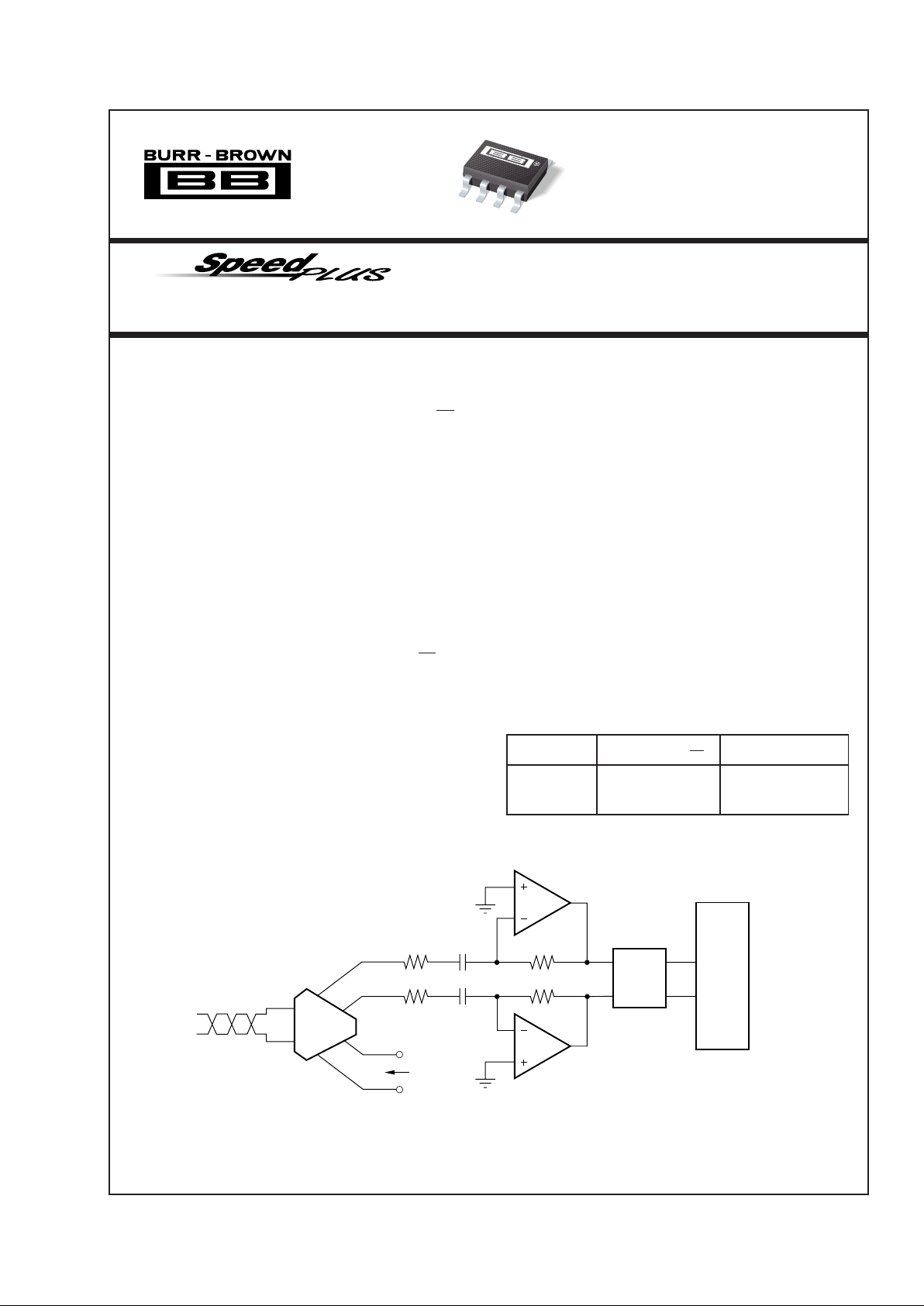
The dual channel OPA2686 provides matched channels
for high speed differencing transimpedance requirements. With over 200MHz bandwidth at a gain of
20dB, excellent gain and phase matching is provided at
IF frequencies for matched I and Q channel amplifiers.
DESCRIPTION
The OPA2686 provides two very low noise, high gain
bandwidth, voltage feedback op amps in a single
package. Operating from a low 12mA/channel quiescent current, each channel provides a 1.4nV/√Hz input
voltage noise with a 1.6GHz gain bandwidth product.
Minimum stable gain is specified at +7V/V while
exceptional flatness is guaranteed at a gain of +10.
The combination of low noise, high slew rate
(600V/µs), and broad bandwidth allow exceptional xDSL
differential receivers to be implemented. Additionally,
de-compensated, low-noise voltage-feedback op amps
are ideal for broadband transimpedance requirements.
FEATURES
● HIGH GAIN BANDWIDTH: 1.6GHz
● LOW INPUT VOLTAGE NOISE: 1.4nV/√Hz
● VERY LOW DISTORTION: –90dBc (5MHz)
● LOW SUPPLY CURRENT: 12mA/chan.
● HIGH CHANNEL ISOLATION: 70dB
● ±5V OPERATION
● STABLE FOR GAINS ≥ +7
OPA2686
1/2
OPA2686
1/2
OPA2686
R
F
R
F
R
G
R
G
Diplexer
Driver
Passive
Filter
Analog
Front
End
Low Noise VDSL Receiver
International Airport Industrial Park • Mailing Address: PO Box 11400, Tucson, AZ 85734 • Street Address: 6730 S. Tucson Blvd., Tucson, AZ 85706 • Tel: (520) 746-1111
Twx: 910-952-1111 • Internet: http://www.burr-brown.com/ • Cable: BBRCORP • Telex: 066-6491 • FAX: (520) 889-1510 • Immediate Product Info: (800) 548-6132
2
®
OPA2686
OPA2686U
TYP GUARANTEED
0°C to –40°C to
MIN/
TEST
PARAMETER CONDITIONS +25°C +25°C
(2)
70°C
(3)
+85°C
(3)
UNITS MAX
LEVEL
(1)
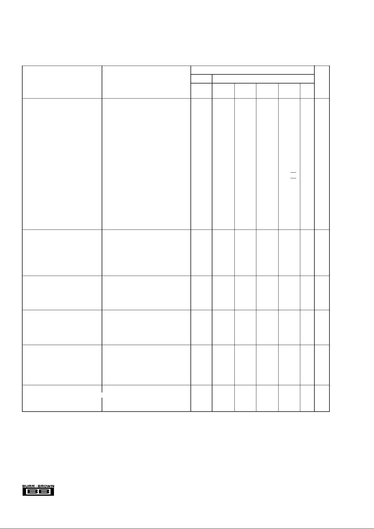
SPECIFICATIONS: VS = ±5V
RF = 453Ω, RL = 100Ω, and G =+10, unless otherwise noted. Figure 1 for AC performance.
AC PERFORMANCE (Figure 1)
Closed-Loop Bandwidth G = +7, R
G
= 50Ω, VO = 200mVp-p 425 MHz typ C
G = +10, R
G
= 50Ω, VO = 200mVp-p 250 200 170 140 MHz min B
G = +20, R
G
= 50Ω, VO = 200mVp-p 100 80 65 55 MHz min B
Gain Bandwidth Product (GBP) G ≥ +40 1600 1250 1100 1000 MHz min B
Bandwidth for 0.1dB Gain Flatness G = +10, R
L
= 100Ω, VO = 200mVp-p 40 35 30 25 MHz min B
Peaking at a Gain of +7 2 dB typ C
Harmonic Distortion G = +10, f = 5MHz, V
O
= 2Vp-p
2nd Harmonic R
L
= 100Ω –72 –67 –65 –60 dBc max B
R
L
= 500Ω –90 –85 –80 –75 dBc max B
3rd Harmonic R
L
= 100Ω –95 –90 –85 –80 dBc max B
R
L
= 500Ω –110 –105 –100 –95 dBc max B
Two-Tone, 3rd-Order Intercept G = +10, f = 10MHz 43 40 39 37 dBm min B
Input Voltage Noise f > 1MHz 1.4 1.6 1.7 1.8 nV/√Hz max B
Input Current Noise f > 1MHz 1.8 2.3 2.4 2.5 pA/√Hz max B
Rise/Fall Time 0.2V Step 1.4 1.75 2 2.5 ns max B
Slew Rate 2V Step 600 500 400 310 V/µs min B
Settling Time to 0.01% 2V Step 18 ns typ C
0.1% 2V Step 16 14 21 25 ns max B
1% 2V Step 11 12 14 18 ns max B
Differential Gain G = +10, NTSC, R
L
= 150Ω 0.02 % typ C
Differential Phase G = +10, NTSC, R
L
= 150Ω 0.02 deg typ C
Channel-to-Channel Crosstalk Input Referred, f = 5MHz –70 dBc typ C
DC PERFORMANCE
(4)
Open-Loop Voltage Gain (AOL)V
O
= 0V 80 75 70 70 dB min A
Input Offset Voltage V
CM
= 0V ±0.35 ±1.0 ±1.2 ±1.5 mV max A
Average Offset Voltage Drift V
CM
= 0V 5 10 µV/°C max B
Input Bias Current V
CM
= 0V –10 –17 –18 –20 µA max A
Input Bias Current Drift V
CM
= 0V 50 100 nA/°C max B
Input Offset Current V
CM
= 0V ±0.5 ±1.0 ±1.5 ±1.8 µA max A
Input Offset Current Drift V
CM
= 0V 5 10 nA/°C max B
INPUT
Common-Mode Input Range (CMIR)
(5)
±3.2 ±3.0 ±2.9 ±2.8 V min A
Common-Mode Rejection (CMR) V
CM
= 0V, Input Referred 100 90 85 75 dB min A
Input Impedance
Differential-Mode V
CM
= 0V 6 || 2 kΩ || pF typ C
Common-Mode V
CM
= 0V 2.9 || 1 MΩ || pF typ C
OUTPUT
Output Voltage Swing ≥ 400Ω Load ±3.5
±3.2 ±3.1 ±3.0 V min A
100Ω Load ±3.3
±3.0 ±2.8 ±2.8 V min A
Current Output, Sourcing V
O
= 0V 80 60 55 50 mA min A
Current Output, Sinking V
O
= 0V –80 –60 –55 –40 mA min A
Closed-Loop Output Impedance G = +10, f = 100kHz 0.008 Ω typ C
POWER SUPPLY
Specified Operating Voltage ±5 V typ C
Maximum Operating Voltage
±6 ±6 ±6 V max A
Max Quiescent Current V
S
= ±5V 24.8 25.8 26 27.8 mA max A
Min Quiescent Current V
S
= ±5V 24.8 23.8 23.8 22 mA min A
Power Supply Rejection Ratio
+PSRR, –PSRR |V
S
| = 4.5 to 5.5, Input Referred 78 70 70 65 dB min A
THERMAL CHARACTERISTICS
Specified Operating Range: U, N Package
–40 to +85
°C typ C
Thermal Resistance,
θ
JA
Junction-to-Ambient
U SO-8 Surface Mount 125 °C/W typ C
NOTES: (1) Test Levels: (A) 100% tested at 25°C. Over temperature limits by characterization and simulation. (B) Limits set by characterization and simulation.
(C) Typical value only for information. (2) Junction temperature = ambient for 25°C guaranteed specifications. (3) Junction temperature = ambient at low temperature
limit: junction temperature = ambient +23°C at high temperature limit for over temperature guaranteed specifications. (4) Current is considered positive out-of-node.
V
CM
is the input common-mode voltage. (5) Tested < 3dB below minimum specified CMR at ±CMIR limits.
3
®
OPA2686
The information provided herein is believed to be reliable; however, BURR-BROWN assumes no responsibility for inaccuracies or omissions. BURR-BROWN assumes
no responsibility for the use of this information, and all use of such information shall be entirely at the user’s own risk. Prices and specifications are subject to change
without notice. No patent rights or licenses to any of the circuits described herein are implied or granted to any third party. BURR-BROWN does not authorize or warrant
any BURR-BROWN product for use in life support devices and/or systems.
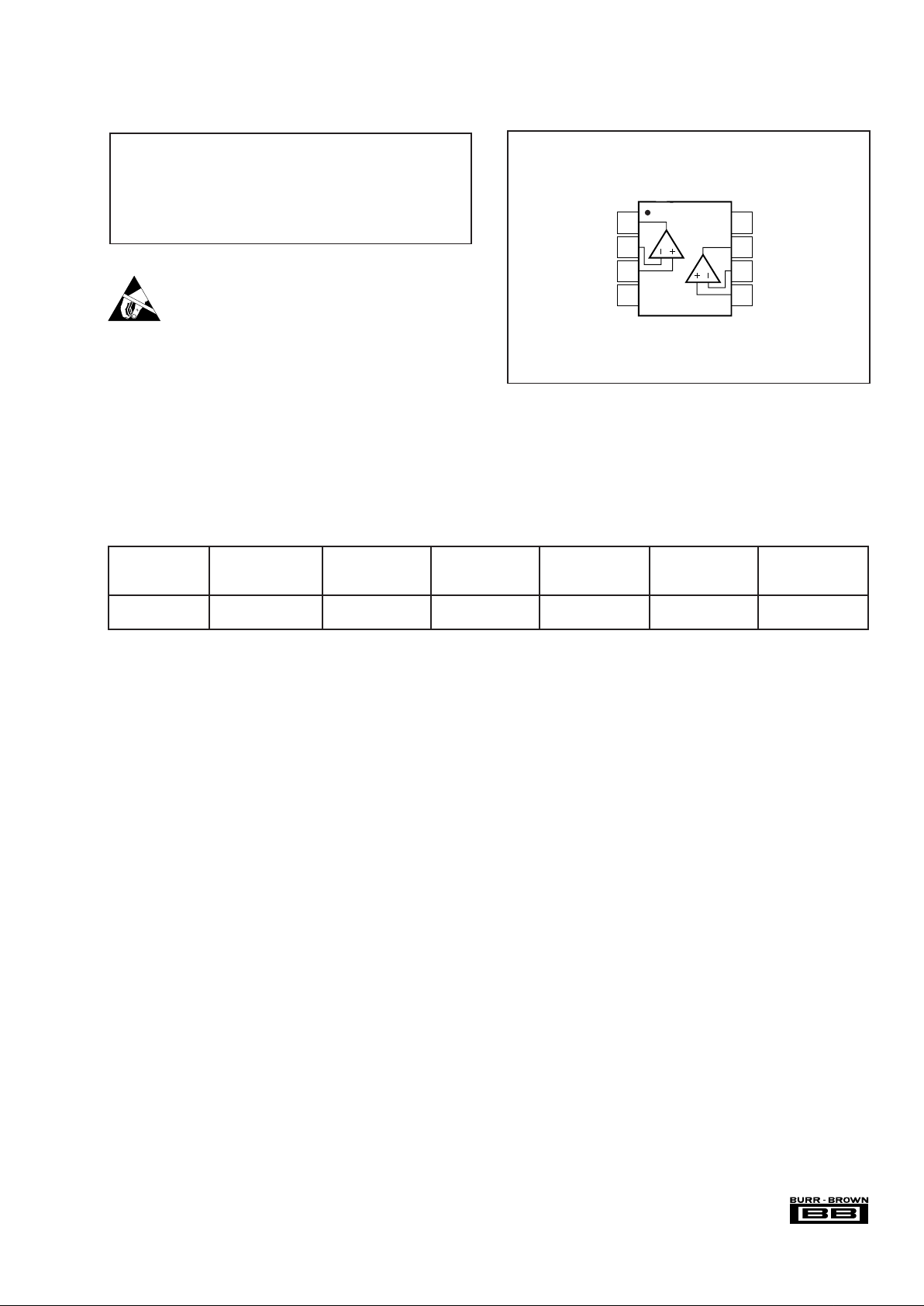
PIN CONFIGURATION
ELECTROSTATIC
DISCHARGE SENSITIVITY
This integrated circuit can be damaged by ESD. Burr-Brown
recommends that all integrated circuits be handled with appropriate
precautions. Failure to observe proper handling and installation
procedures can cause damage.
ESD damage can range from subtle performance degradation to
complete device failure. Precision integrated circuits may be more
susceptible to damage because very small parametric changes
could cause the device not to meet its published specifications.
PACKAGE
DRAWING TEMPERATURE PACKAGE ORDERING TRANSPORT
PRODUCT PACKAGE NUMBER RANGE MARKING NUMBER
(1)
MEDIA
OPA2686U SO-8 Surface Mount 182 –40°C to +85°C OPA2686U OPA2686U Rails
" """"OPA2686U/2K5 Tape and Reel
NOTES: (1) Models with a slash (/) are available only in Tape and Reel in the quantities indicated (e.g., /2K5 indicates 2500 devices per reel). Ordering 2500 pieces
of “OPA2686U/2K5” will get a single 2500-piece Tape and Reel.
PACKAGE/ORDERING INFORMATION
ABSOLUTE MAXIMUM RATINGS
Power Supply ............................................................................... ±6.5V
DC
Internal Power Dissipation ...................................... See Thermal Analysis
Differential Input Voltage .................................................................. ±1.2V
Input Voltage Range ............................................................................ ±V
S
Storage Temperature Range: U..................................... –40°C to +125°C
Lead Temperature (soldering, 10s) .............................................. +300°C
Junction Temperature (T
J
) ........................................................... +175°C
Top View SO-8
1
2
3
4
8
7
6
5
V+
Out B
–In B
+In B
Out A
–In A
+In A
V–
OPA2686
4
®
OPA2686
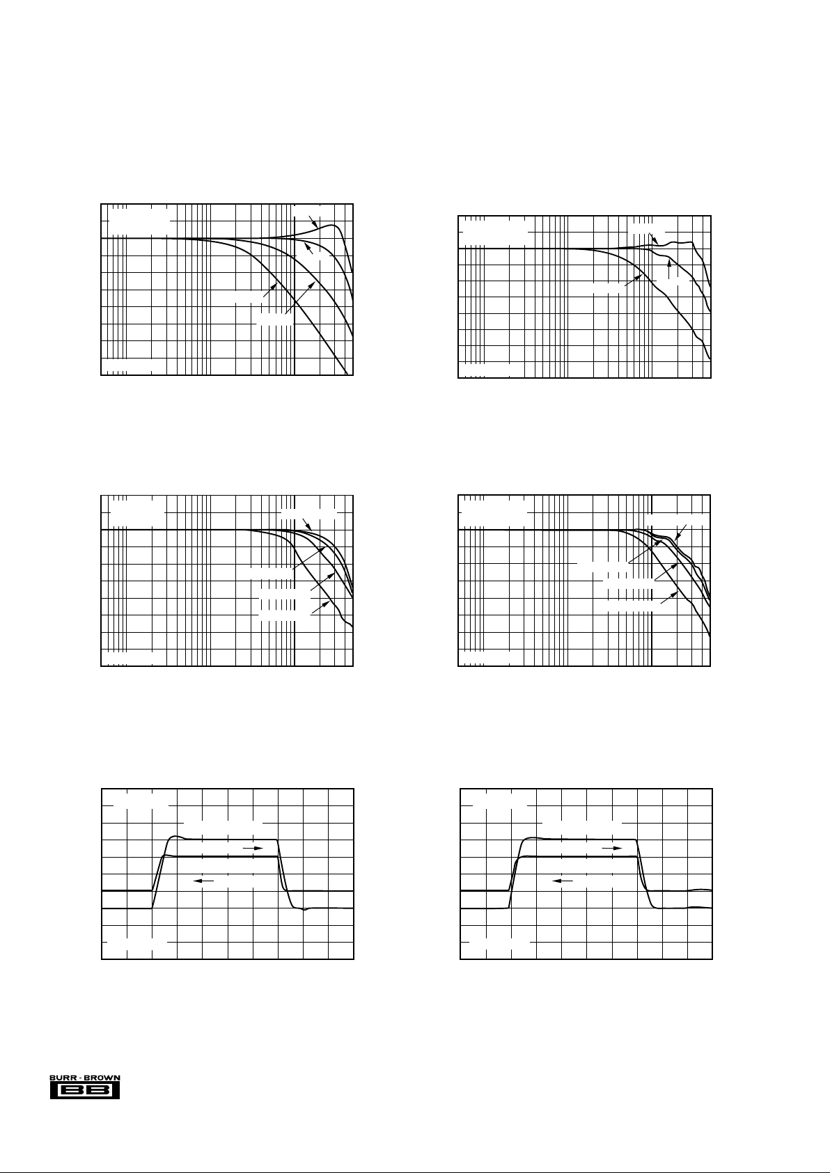
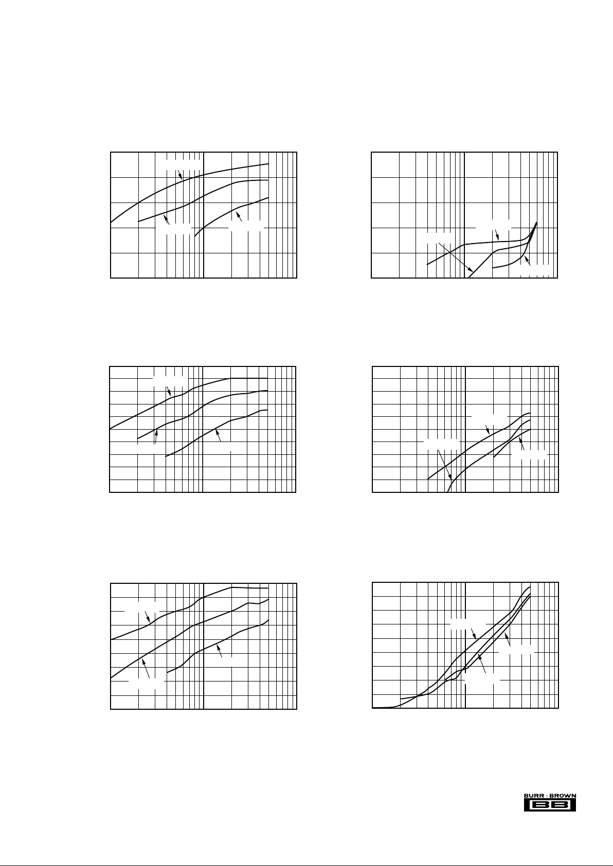
TYPICAL PERFORMANCE CURVES: VS = ±5V
At TA = +25°C, G = +10, RF = 453Ω, and RL = 100Ω, unless otherwise noted.
6
3
0
–3
–6
–9
–12
–15
–18
–21
–24
NON-INVERTING SMALL-SIGNAL
FREQUENCY RESPONSE
Frequency (MHz)
Normalized Gain (3dB/div)
0.5 10 100 500
G = +50
See Figure 1
RG = 50Ω
V
O
= 0.2Vp-p
G = +20
G = +7
G = +10
6
3
0
–3
–6
–9
–12
–15
–18
–21
–24
INVERTING SMALL-SIGNAL
FREQUENCY RESPONSE
Frequency (MHz)
Normalized Gain (3dB/div)
0.5 10 100 500
RG = RS = 50Ω
V
O
= 0.2Vp-p
G = –12
G = –50
G = –20
See Figure 2
26
23
20
17
14
11
8
5
2
–1
–4
NON-INVERTING LARGE-SIGNAL
FREQUENCY RESPONSE
Frequency (MHz)
Gain (3dB/div)
0.5 10 100 500
RG = 50Ω
G = +10V/V
VO = 0.2Vp-p
VO = 1Vp-p
VO = 2Vp-p
V
O
= 5Vp-p
See Figure 1
100
0
–100
1.5
1.0
0.5
0
–0.5
–1.0
–1.5
NON-INVERTING PULSE RESPONSE
Time (5ns/div)
Output Voltage (100mV/div)
Output Voltage (500mV/div)
G = +10V/V
Large Signal ±1V
Small Signal ±100mV
Right Scale
Left Scale
See Figure 1
100
0
–100
1.5
1.0
0.5
0
–0.5
–1.0
–1.5
INVERTING PULSE RESPONSE
Time (5ns/div)
Output Voltage (100mV/div)
Output Voltage (500mV/div)
G = –20V/V
Large Signal ±1V
Small Signal ±100mV
Right Scale
Left Scale
See Figure 2
30
29
26
23
20
17
14
11
8
5
2
INVERTING LARGE-SIGNAL
FREQUENCY RESPONSE
Frequency (MHz)
Gain (3dB/div)
0.1 10 100 500
RG = RS = 50Ω
G = –20V/V
VO = 0.2Vp-p
VO = 1Vp-p
VO = 2Vp-p
V
O
= 5Vp-p
See Figure 2
5
®
OPA2686
TYPICAL PERFORMANCE CURVES: VS = ±5V (Cont.)
At TA = +25°C, G = +10, RF = 453Ω, and RL = 100Ω, unless otherwise noted. See Figure 1.
–60
–70
–80
–90
–100
–110
Output Voltage (Vp-p)
0.1 101
5MHz 2nd HARMONIC DISTORTION
vs OUTPUT VOLTAGE
2nd Harmonic Distortion (dBc)
RL = 100Ω
RL = 500Ω
RL = 200Ω
–60
–70
–80
–90
–100
–110
Output Voltage (Vp-p)
0.1 101
5MHz 3rd HARMONIC DISTORTION
vs OUTPUT VOLTAGE
3rd Harmonic Distortion (dBc)
RL = 500Ω
RL = 200Ω
RL = 100Ω
–55
–60
–65
–70
–75
–80
–85
–90
–95
–100
–105
Output Voltage (Vp-p)
0.1 101
10MHz 2nd HARMONIC DISTORTION
vs OUTPUT VOLTAGE
2nd Harmonic Distortion (dBc)
RL = 200Ω
RL = 100Ω
RL = 500Ω
–55
–60
–65
–70
–75
–80
–85
–90
–95
–100
–105
Output Voltage (Vp-p)
0.1 101
10MHz 3rd HARMONIC DISTORTION
vs OUTPUT VOLTAGE
3rd Harmonic Distortion (dBc)
RL = 100Ω
RL = 200Ω
RL = 500Ω
–50
–55
–60
–65
–70
–75
–80
–85
–90
–95
Output Voltage (Vp-p)
0.1 101
20MHz 2nd HARMONIC DISTORTION
vs OUTPUT VOLTAGE
2nd Harmonic Distortion (dBc)
RL = 200Ω
RL = 100Ω
RL = 500Ω
–50
–55
–60
–65
–70
–75
–80
–85
–90
–95
Output Voltage (Vp-p)
0.1 101
20MHz 3rd HARMONIC DISTORTION
vs OUTPUT VOLTAGE
3rd Harmonic Distortion (dBc)
RL = 200Ω
RL = 100Ω
RL = 500Ω
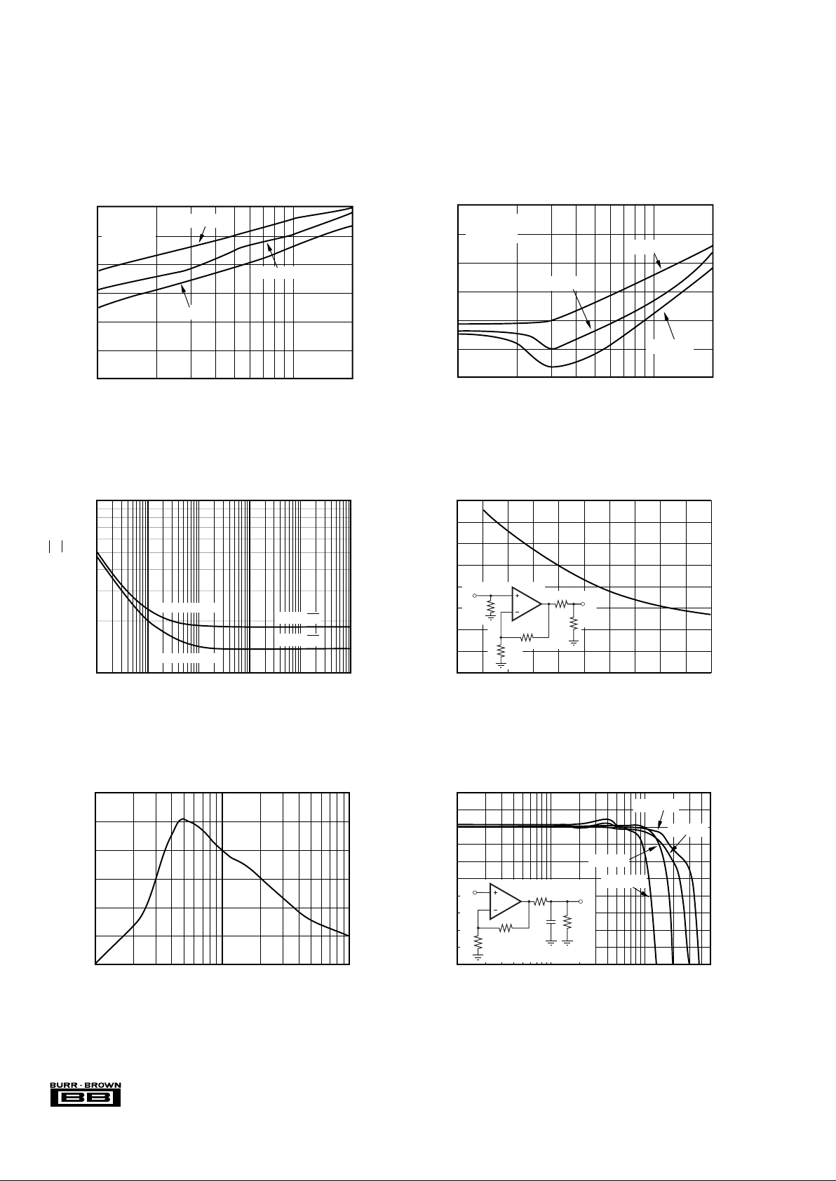
6
®
OPA2686
TYPICAL PERFORMANCE CURVES: VS = ±5V (Cont.)
At TA = +25°C, G = +10, RF = 453Ω, and RL = 100Ω, unless otherwise noted. See Figure 1.
60
50
40
30
20
10
0
R
S
vs CAPACITIVE LOAD
Capacitive Load (pF)
1 10 100
R
S
(Ω)
22
21
20
19
18
17
16
15
14
13
12
Frequency (MHz)
FREQUENCY RESPONSE vs CAPACITIVE LOAD
1 10010 500
Gain to Capacitive Load (1dB/div)
CL = 10pF
CL = 50pF
CL = 20pF
CL = 100pF
OPA2686
R
S
V
IN
V
O
C
L
1kΩ
453Ω
50Ω
1kΩ is optional
–45
–55
–65
–75
–85
–95
–105
Frequency (MHz)
12010
2nd HARMONIC DISTORTION
vs FREQUENCY
2nd Harmonic Distortion (dBc)
VO = 2Vp-p
R
L
= 100Ω
G = +50V
G = +20
G = +10
50
45
40
35
30
25
20
15
0
TWO-TONE, 3rd-0RDER INTERMODULATION
INTERCEPT vs FREQUENCY
Frequency (MHz)
0 5 10 15 20 25 30 35 40 45 50
Intercept (dBm)
OPA2686
P
I
P
O
50Ω
50Ω
50Ω
453Ω
50Ω
–45
–55
–65
–75
–85
–95
–105
Frequency (MHz)
12010
3rd HARMONIC DISTORTION
vs FREQUENCY
3rd Harmonic Distortion (dBc)
VO = 2Vp-p
R
L
= 100Ω
G = +10
G = +50
G = +20
10
1
INPUT VOLTAGE and CURRENT NOISE DENSITY
Frequency (Hz)
100 10M1k 10k 100k 1M
Current Noise (pA/√Hz)
Voltage Noise (nV/√Hz)
1.8pA/√Hz
1.4nV/√Hz
Current Noise
Voltage Noise
 Loading...