

Burr Brown OPA2677N, OPA2677U, OPA2677U-2K5, OPA2677H Datasheet
Dual, Wideband, High Output Current
OPERATIONAL AMPLIFIER
DESCRIPTION
The OPA2677 provides the high output current and low distortion
required in emerging ADSL and HDSL2 driver applications.
Operating on a single +12V supply, the OPA2677 consumes a
low 9mA/chan quiescent current to deliver a very high 500mA
peak output current. Guaranteed output current supports even the
most demanding ADSL CPE requirements with > 380mA minimum output current with low harmonic distortion. Differential
driver applications will deliver < –85dBc distortion at the peak
upstream power levels of full rate ADSL. The high 200MHz
bandwidth will also support the most demanding VDSL line
driver requirements.
OPA2677
®
FEATURES
●
WIDEBAND +12V OPERATION: 200MHz (G = +4)
● UNITY GAIN STABLE: 220MHz (G = 1)
● HIGH OUTPUT CURRENT: 500mA
● OUTPUT VOLTAGE SWING: ±5V
● HIGH SLEW RATE: 1800V/µs
● LOW SUPPLY CURRENT: 18mA
● FLEXIBLE POWER CONTROL
APPLICATIONS
● xDSL LINE DRIVER
● CABLE MODEM DRIVER
● MATCHED I/Q CHANNEL AMPLIFIER
● BROADBAND VIDEO LINE DRIVER
● ARB LINE DRIVER
● PERFORMANCE UPGRADE TO AD8017
Power control features are included in the SO-14 package version
to allow system power to be minimized. Two logic control lines
allow four quiescent power settings. These include full power,
power cutback for short loops, idle state for no signal transmission
but line match maintenance, and shutdown for power off with a
high impedance output.
Specified on ±6V supplies (to support +12V operation), the
OPA2677 will also support a single +5V or dual ±5V supply.
Video applications will benefit from its very high output
current to drive up to 10 parallel video loads (15Ω) with < 0.1%/
0.1° dG/dØ non-linearity.
TM
International Airport Industrial Park • Mailing Address: PO Box 11400, Tucson, AZ 85734 • Street Address: 6730 S. Tucson Blvd., Tucson, AZ 85706 • Tel: (520) 746-1111
Twx: 910-952-1111 • Internet: http://www.burr-brown.com/ • Cable: BBRCORP • Telex: 066-6491 • FAX: (520) 889-1510 • Immediate Product Info: (800) 548-6132
OPA2677 RELATED PRODUCTS
SINGLES DUALS TRIPLES NOTES
OPA681 OPA2681 OPA3681 Single +12V Capable
— OPA2607 — ±12V Capable
©
2000 Burr-Brown Corporation PDS-1593A Printed in U.S.A. April, 2000
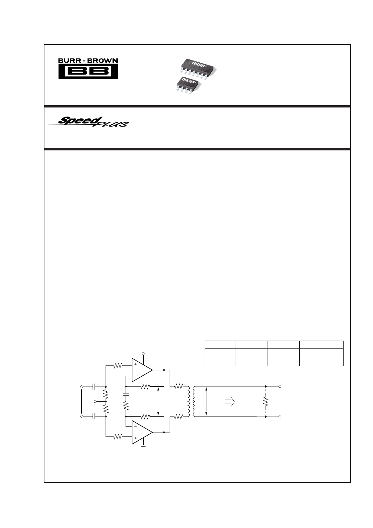
Single Supply ADSL Upstream Driver
82.5Ω
2kΩ
2kΩ
1µF
17.4Ω
100Ω
2Vp-p
AFE
Output
324Ω
20Ω
324Ω
1/2
OPA2677
1/2
OPA2677
+12V
1:1.7
15Vp-p Twisted Pair17.7Vp-p
20Ω
17.4Ω
+6.0V
OPA2677
OPA2677
For most current data sheet and other product
information, visit www.burr-brown.com
2
®
OPA2677
SPECIFICATIONS: VS = ±6V
At TA = +25°C, G = +4, RF = 402Ω, and RL = 100Ω, unless otherwise noted. See Figure 1 for AC performance only
OPA2677U, H, N
TYP GUARANTEED
0°C to –40°C to
MIN/
TEST
PARAMETER CONDITIONS +25°C +25°C
(2)
70°C
(3)
+85°C
(3)
UNITS MAX
LEVEL
(1)
AC PERFORMANCE (Figure 1)
Small-Signal Bandwidth (VO = 0.5Vp-p) G = +1, RF = 511Ω 220 MHz typ C
G = +2, R
F
= 475Ω 200 MHz typ C
G = +4, R
F
= 402Ω 200 MHz typ C
G = +8, R
F
= 250Ω 250 MHz typ C
Bandwidth for 0.1dB Gain Flatness G = +4, V
O
= 0.5Vp-p 80 MHz typ C
Large-Signal Bandwidth G = +4, V
O
= 5Vp-p 200 MHz typ C
Slew Rate G = +4, 5V Step 1800 V/µs typ C
Rise/Fall Time G = +4, V
O
= 2V Step 2 ns typ C
Spurious Free Dynamic Range V
O
= 2Vp-p, 5MHz, 100Ω 74 dB typ C
V
O
= 2Vp-p, 100kHz, 100Ω 96 dB typ C
Input Voltage Noise 2.0 nV/√Hz typ C
Non-Inverting Input Current Noise 14 pA/√Hz typ C
Inverting Input Current Noise 21 pA/√Hz typ C
Differential Gain NTSC, G = +2, R
L
= 150Ω 0.03 % typ C
NTSC, G = +2, R
L
= 37.5Ω 0.05 % typ C
Differential Phase NTSC, G = +2, R
L
= 150Ω 0.01 degrees typ C
NTSC, G = +2, R
L
= 37.5Ω 0.04 degrees typ C
Channel-to-Channel Crosstalk f = 5MHz, Input Referred –80 dB typ C
DC PERFORMANCE
(4)
Open-Loop Transimpedance Gain
VO = 0V, RL = 100Ω 135 95 90 85 kΩ min A
Input Offset Voltage V
CM
= 0V ±1.0 ±5.5 ±7 ±7.5 mV max A
Average Offset Voltage Drift V
CM
= 0V 35 40 µV/°C max B
Non-Inverting Input Bias Current V
CM
= 0V ±10 ±30 ±45 ±55 µA max A
Average Non-Inverting Input Bias Current Drift V
CM
= 0V 250 350 nA/°C max B
Inverting Input Bias Current VCM = 0V ±10 ±30 ±45 ±55 µA max A
Average Inverting Input Bias Current Drift V
CM
= 0V 250 350 nA°/C max B
INPUT
(4)
Common-Mode Input Range (CMIR)
(5)
±4.5 ±4.2 ±4.1 ±4.0 V min A
Common-Mode Rejection Ratio(CMRR) V
CM
= 0V, Input Referred 55 52 51 50 dB min A
Non-Inverting Input Impedance 250 || 2 kΩ || pF typ C
Minimum Inverting Input Resistance
Open-Loop 22 14 Ω min B
Maximum Inverting Input Resistance
Open-Loop 22 30 Ω max B
OUTPUT
(4)
Voltage Output Swing No Load ±5.1 ±4.9 ±4.8 ±4.7 V min A
R
L
= 100Ω±5.0 ±4.8 ±4.7 ±4.5 V min A
R
L
= 25Ω±4.8 V typ C
Current Output, Sourcing VO = 0 500 380 340 290 mA min A
Current Output, Sinking V
O
= 0 500 380 340 290 mA min A
Closed-Loop Output Impedance G = +4, f = 100kHz 0.003 Ω typ C
Power Control
(SO-14 only)
Maximum Logic 0 A0, A1 1.8 1.0 V max A
Minimum Logic 1 A0, A1 2.3 2.6 V min A
Logic Input Current A0 = A1 = 0 50 100 µA max A
Supply Current at Full Power A0 = 1, A1 = 1 18 mA typ C
Supply Current at Power Cutback A0 = 0, A1 = 1 13.5 mA typ C
Supply Current at Idle Power A0 = 1, A1 = 0 3.8 mA typ C
Supply Current at Shutdown A0 = 0, A1 = 0 0.8 mA typ C
Output Impedance in Idle Power G = +4, f = 100kHz 0.1 Ω typ C
Output Impedance in Shutdown 100 || 4 kΩ || pF typ C
Supply Current Step Time 10% to 90% Change 200 ns typ C
Output Switching Glitch Inputs at GND ±20 mV typ C
Shutdown Isolation G = +4, 1MHz, A0 = 0, A1 = 0 85 dB typ C
POWER SUPPLY
Specified Operating Voltage ±6 V typ C
Maximum Operating Voltage ±6.3 ±6.3 ±6.3 V max A
Maximum Quiescent Current V
S
= ±6V, Full Power 18 18.5 19 19.5 mA max A
Minimum Quiescent Current V
S
= ±6V, Full Power 18 17.5 16.6 16.3 mA min A
Power Supply Rejection Ratio (PSRR) f = 100kHz, Input Referred 56 52 50 49 dB min A
TEMPERATURE RANGE
Specification: U, N
–40 to +85
°C
Thermal Resistance,
θ
JA
U SO-8 Junction-to-Ambient 125 °C/W
H PSO-8 55 °C/W
N SO-14 100 °C/W
NOTES: (1) Test Levels: (A) 100% tested at 25°C. Over temperature limits by characterization and simulation. (B) Limits set by characterization and simulation.
(C) Typical value only for information. (2) Junction temperature = ambient for 25°C guaranteed specifications. (3) Junction temperature = ambient at low temperature
limit: junction temperature = ambient +23°C at high temperature limit for over temperature guaranteed specifications. (4) Current is considered positive-out-of node.
V
CM
is the input common-mode voltage. (5) Tested < 3dB below minimum CMRR limit at ± CMIR limits.
3
®
OPA2677
SPECIFICATIONS: VS = +5V
At TA = +25°C, G = +2, RF = 453Ω, and RL = 100Ω, unless otherwise noted. See Figure 2 for AC performance only
OPA2677U, H, N
TYP GUARANTEED
0°C to –40°C to
MIN/
TEST
PARAMETER CONDITIONS +25°C +25°C
(2)
70°C
(3)
+85°C
(3)
UNITS MAX
LEVEL
(1)
AC PERFORMANCE (Figure 2)
Small-Signal Bandwidth (V
O
= 0.5Vp-p) G = +1, RF = 536Ω 160 MHz typ C
G = +2, R
F
= 511Ω 150 MHz typ C
G = +4, RF = 453Ω 160 MHz typ C
G = +8, R
F
= 332Ω 160 MHz typ C
Bandwidth for 0.1dB Gain Flatness G = +4, V
O
= 0.5Vp-p 70 MHz typ C
Large-Signal Bandwidth G = +4, V
O
= 2Vp-p 100 MHz typ C
Slew Rate G = +4, 2V Step 1100 V/µs typ C
Rise/Fall Time G = +4, V
O
= 2V Step 2 ns typ C
Spurious Free Dynamic Range VO = 2Vp-p, 5MHz, 100Ω 67 dB typ C
V
O
= 2Vp-p, 100kHz, 100Ω 87 dB typ C
Input Voltage Noise 2.0 nV/√Hz typ C
Non-Inverting Input Current Noise 14 pA/√Hz typ C
Inverting Input Current Noise 21 pA/√Hz typ C
Channel-to-Channel Crosstalk f = 5MHz, Input Referred –80 dB typ C
DC PERFORMANCE
(4)
Open-Loop Transimpedance Gain
VO = 0V, RL = 100Ω 125 90 85 80 kΩ min A
Input Offset Voltage V
CM
= 0V ±0.8 ±4.0 ±5.5 ±6.0 mV max A
Average Offset Voltage Drift V
CM
= 0V 35 40 µV/°C max B
Non-Inverting Input Bias Current V
CM
= 0V ±10 ±30 ±45 ±55 µA max A
Average Non-Inverting Input Bias Current Drift V
CM
= 0V 250 350 nA/°C max B
Inverting Input Bias Current VCM = 0V ±10 ±30 ±45 ±55 µA max A
Average Inverting Input Bias Current Drift V
CM
= 0V 250 350 nA°/C max B
INPUT
(4)
Most Positive Input Voltage 3.7 3.4 3.3 3.2 V min A
Least Positive Input Voltage 1.3 1.6 1.7 1.8 V max A
Common-Mode Rejection Ratio(CMRR) V
CM
= 2.5V, Input Referred 52 50 49 48 dB min A
Non-Inverting Input Impedance 250 || 2 kΩ || pF typ C
Minimum Inverting Input Resistance
Open-Loop 29 20 Ω min B
Maximum Inverting Input Resistance
Open-Loop 29 37 Ω max B
OUTPUT
(4)
Most Positive Output Voltage No Load 4.2 4.0 3.9 3.7 V min A
R
L
= 100Ω 4.0 3.9 3.8 3.6 V min A
Least Positive Output Voltage No Load 0.8 1.0 1.1 1.3 V max A
R
L
= 100Ω 1.0 1.1 1.2 1.5 V max A
Current Output, Sourcing V
O
= 2.5V 300 200 160 120 mA min A
Current Output, Sinking V
O
= 2.5V 300 200 160 120 mA min A
Closed-Loop Output Impedance G = +4, f = 100kHz 0.02 Ω typ C
Power Control
(SO-14 only)
Maximum Logic 0 A0, A1 1.8 1.0 V max A
Minimum Logic 1 A0, A1 2.3 2.6 V min A
Logic Input Current A0 = A1 = 0 50 100 µA max A
Supply Current at Full Power A0 = 1, A1 = 1 13.5 mA typ C
Supply Current at Power Cutback A0 = 0, A1 = 1 11 mA typ C
Supply Current at Idle Power A0 = 1, A1 = 0 2 mA typ C
Supply Current at Shutdown A0 = 0, A1 = 0 0.8 mA typ C
Output Impedance in Idle Power G = +4, f = 100kHz 0.1 Ω typ C
Output Impedance in Shutdown 100 || 4 kΩ || pF typ C
Supply Current Step Time 10% to 90% Change 200 ns typ C
Output Switching Glitch Inputs at GND ±20 mV typ C
Shutdown Isolation G = +4, 1MHz, A0 = 0, A1 = 0 85 dB typ C
POWER SUPPLY
Specified Operating Voltage +5 V typ C
Maximum Operating Voltage +12.6 +12.6 +12.6 V max A
Maximum Quiescent Current V
S
= +5V, Full Power 13.5 14.5 15 15.5 mA max A
Minimum Quiescent Current V
S
= +5V, Full Power 13.5 12.5 12 11.5 mA min A
Power Supply Rejection Ratio (PSRR) f = 100kHz, Input Referred 52 dB typ C
TEMPERATURE RANGE
Specification: U, N
–40 to +85
°C
Thermal Resistance,
θ
JA
U SO-8 Junction-to-Ambient 125 °C/W
H PSO-8 55 °C/W
N SO-14 100 °C/W
NOTES: (1) Test Levels: (A) 100% tested at 25°C. Over temperature limits by characterization and simulation. (B) Limits set by characterization and simulation.
(C) Typical value only for information. (2) Junction temperature = ambient for 25°C guaranteed specifications. (3) Junction temperature = ambient at low temperature
limit: junction temperature = ambient +23°C at high temperature limit for over temperature guaranteed specifications. (4) Current is considered positive-out-of node.
V
CM
is the input common-mode voltage. (5) Tested < 3dB below minimum specified CMRR at ± CMIR limits.
4
®
OPA2677
ABSOLUTE MAXIMUM RATINGS
Power Supply .............................................................................. ±6.5VDC
Internal Power Dissipation
(1)
............................ See Thermal Information
Differential Input Voltage ..................................................................±1.2V
Input Voltage Range ............................................................................ ±V
S
Storage Temperature Range: U, N, H ........................... –40°C to +125°C
Lead Temperature (soldering, 10s) .............................................. +300°C
Junction Temperature (T
J
) ........................................................... +175°C
NOTE:: (1) Packages must be derated based on specified
θ
JA
. Maximum T
J
must be observed.
ELECTROSTATIC
DISCHARGE SENSITIVITY
Electrostatic discharge can cause damage ranging from performance degradation to complete device failure. Burr-Brown
Corporation recommends that all integrated circuits be handled
and stored using appropriate ESD protection methods.
ESD damage can range from subtle performance degradation to
complete device failure. Precision integrated circuits may be
more susceptible to damage because very small parametric
changes could cause the device not to meet published specifications.
The information provided herein is believed to be reliable; however, BURR-BROWN assumes no responsibility for inaccuracies or omissions. BURR-BROWN assumes
no responsibility for the use of this information, and all use of such information shall be entirely at the user’s own risk. Prices and specifications are subject to change
without notice. No patent rights or licenses to any of the circuits described herein are implied or granted to any third party. BURR-BROWN does not authorize or warrant
any BURR-BROWN product for use in life support devices and/or systems.
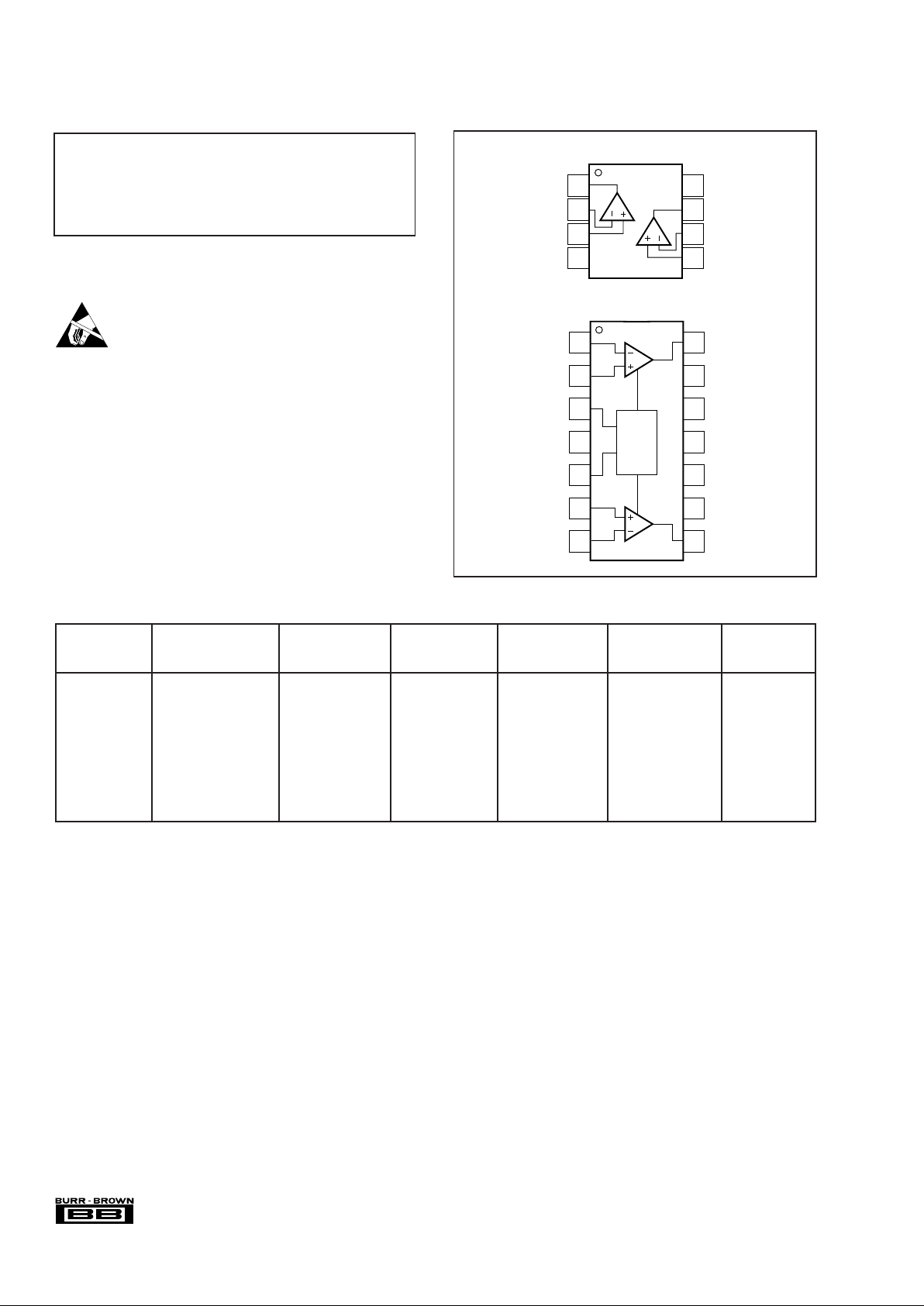
PIN CONFIGURATIONS
Top View SO-8, PSO-8
SO-14
PACKAGE SPECIFIED
DRAWING TEMPERATURE PACKAGE ORDERING TRANSPORT
PRODUCT PACKAGE NUMBER RANGE MARKING NUMBER
(1)
MEDIA
OPA2677U SO-8 Surface Mount 182 –40°C to +85°C OPA2677U OPA2677U Rails
"""""OPA2677U/2K5 Tape and Reel
OPA2677H PSO-8 Surface Mount 182-1 –40°C to +85°C OPA2677H — Rails
"""""— Tape and Reel
OPA2677N SO-14 Surface Mount 235 –40°C to –85°C OPA2677N — Rails
"""""— Tape and Reel
NOTE: (1) Models with a slash (/) are available only as Tape and Reel in the quantity indicated after the slash (e.g. /2K5 indicates 2500 devices per reel). Ordering 2500
pieces of the OPA2677U/2K5 will get a single 2500-piece Tape and Reel.
PACKAGE/ORDERING INFORMATION
1
2
3
4
8
7
6
5
+V
S
Out B
–In B
+In B
OPA2677U, H
Out A
–In A
+In A
–V
S
1
2
3
4
5
6
7
14
13
12
11
10
9
8
–In A
+In A
A0
–V
S
A1
+In B
–In B
Out A
NC
NC
+V
S
NC
NC
Out B
Power
Control
OPA2677N
 Loading...