

Burr Brown OPA2662AU Datasheet
OPA2662
OPA2662
OPA2662
Dual, Wide Bandwidth
OPERATIONAL TRANSCONDUCTANCE AMPLIFIER
FEATURES
● 370MHz BANDWIDTH
● 58mA/ns SLEW RATE
● HIGH OUTPUT CURRENT:
±75mA
● 400Mbit/s DATA RATE
● VOLTAGE-CONTROLLED CURRENT
SOURCE
● ENABLE/DISABLE FUNCTION
APPLICATIONS
● HEAD DRIVE AMPLIFIER FOR ANALOG/
DIGITAL VIDEO TAPES AND DATA RECORDERS
● LED AND LASER DIODE DRIVER
● HIGH CURRENT VIDEO BUFFER OR LINE
DRIVER
● RF OUTPUT STAGE DRIVER
● HIGH DENSITY DISK DRIVES
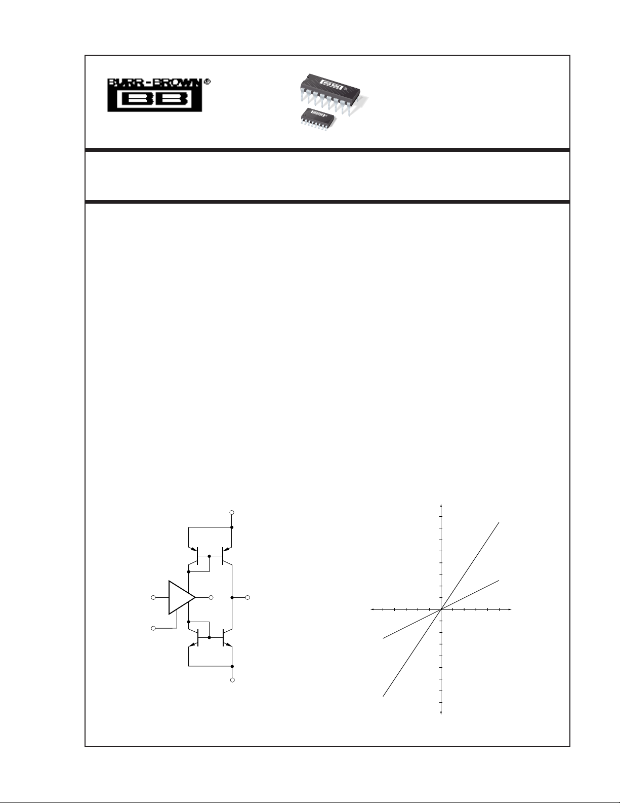
+V
CCOUT
(16)
–V
C
(11,14)
(9)
CCOUT
B
(2,7)
EN
(3, 6)
+1
1/2 OPA2662
E
(10,15)
DESCRIPTION
The OPA2662 is a versatile driver device for ultra
wide-bandwidth systems, including high-resolution
video, RF and IF circuitry, communications and test
equipment. The OPA2662 includes two power voltage-controlled current sources, or operational
transconductance amplifiers (OTAs), in a 16-pin DIP
or SOL-16 package and is specified for the extended
industrial temperature range (–40°C to +85°C). The
output current is zero-for-zero differential input voltage. The OTAs provide a 250MHz large-signal bandwidth, a 58mA/ns slew rate, and each current source
delivers up to ±75mA output current.
The transconductance of both OTAs can be adjusted
between pin 5 and –V
allowing bandwidth, quiescent current, harmonic distortion and gain trade-offs to be optimized. The output current can be set with a degeneration resistor
between the emitter and GND. The current mirror
ratio between the collector and emitter currents is
fixed to three. Switching stages compatible to logic
TTL levels make it possible to turn each OTA separately on within 30ns and off within 200ns at full
power.
by an external resistor,
CC
I (mA)
80
70
60
50
40
30
20
0.2–0.4–0.6 0.4 0.6 0.8 1–0.8–1
–10
–20
–30
–40
–50
–60
–70
–80
I
C
I
E
V
IN
OTA Transfer
Characteristics
(V)
International Airport Industrial Park • Mailing Address: PO Box 11400, Tucson, AZ 85734 • Street Address: 6730 S. Tucson Blvd., Tucson, AZ 85706 • Tel: (520) 746-1111 • Twx: 910-952-1111
Internet: http://www.burr-brown.com/ • FAXLine: (800) 548-6133 (US/Canada Only) • Cable: BBRCORP • Telex: 066-6491 • FAX: (520) 889-1510 • Immediate Product Info: (800) 548-6132
©
1991 Burr-Brown Corporation PDS-1129D Printed in U.S.A. August, 1994
SPECIFICATIONS
ELECTRICAL
DC-SPECIFICATIONS
At VCC = ±5V, RQ = 750Ω, TA = +25°C, and configured as noted under “CONDITIONS”.
OPA2662AP, AU
PARAMETER CONDITIONS MIN TYP MAX UNITS
OTA INPUT OFFSET VOLTAGE
Initial R
vs Temperature 35 µV/°C
vs Supply (tracking) V
vs Supply (non-tracking) V
vs Supply (non-tracking) V
Matching 2 ±7mV
CC
CC
CC
OTA B-INPUT BIAS CURRENT
Initial R
vs Temperature –5 nA/°C
vs Supply (tracking) V
vs Supply (non-tracking) V
vs Supply (non-tracking) V
Matching 0.2 ±1 µA
CC
CC
CC
OTA C-OUTPUT BIAS CURRENT R
Initial 0.5 –0.5/+1.5 mA
vs Temperature 1.5 µA/°C
vs Supply (tracking) V
vs Supply (non-tracking) V
vs Supply (non-tracking) V
Matching 0.06 ±0.5 mA
B-INPUT IMPEDANCE
Impedance I
OTA INPUT NOISE
Input Noise Voltage Density f = 20kHz to 100MHz 4.4 nV/√Hz
Output Noise Current Density 0.09 nA/√Hz
Signal-to-Noise Ratio S/N = 20 log • (0.7/V
OTA C-RATED OUTPUT
Output Voltage Compliance I
Output Current R
Output Impedance, r
C
OTA E-RATED OUTPUT
Voltage Output R
DC Current Output R
Voltage Gain V
Output Impedance, r
E
POWER SUPPLY
Rated Voltage R
Derated Performance R
Positive Quiescent Current R
for both OTAs
Positive Quiescent Current R
for both OTAs
(4)
(4)
Quiescent Current Range Programmable
TEMPERATURE RANGE
Specification Ambient Temperature –40 +85 °C
Thermal Resistance,
AP 90 °C/W
θ
JA
AU 100 °C/W
NOTES: (1) Characterization sample. (2) “Typical Values” are Mean values. The average of the two amplifiers is used for amplifier specific parameters. (3) “Min”
and “Max” Values are mean ±3 Standard Deviations. Worst case of the two amplifiers (Mean ±3 Standard Deviations) is used for amplifier specific parameters. (4)
–
I
typically 2mA less than I
Q
+
due to OTA C-Output Bias Current and TTL Select Circuit Current.
Q
= 50kΩ, RC = 40Ω 12 ±30 mV
E
= ±4.5V to ±5.5V, RE = 50kΩ, RC = 1kΩ 27 dB
= +4.5V to +5.5V, RE = 50kΩ, RC = 1kΩ 15 dB
= –4.5V to –5.5V, RE = 50kΩ, RC = 1kΩ 40 dB
= 100Ω, RC = 40Ω 1 –1/+5 µA
E
= ±4.5V to ±5.5V, RE = 50kΩ, RC = 1kΩ 60 nA/V
= +4.5V to +5.5V, RE = 50kΩ, RC = 1kΩ 160 nA/V
= –4.5V to –5.5V, RE = 50kΩ, RC = 1kΩ 40 nA/V
= 100Ω, RC = 1kΩ
E
= ±4.5V to ±5.5V 72 µA/V
CC
= +4.5V to +5.5V 236 µA/V
CC
= –4.5V to –5.5V 92 µA/V
CC
= ±17mA 4.5 || 1.5 MΩ || pF
Q
• √5MHz) 97 dB
N
= ±5mA, RE = 100Ω, RC = 1kΩ±3.4 V
C
= 40Ω, RE = 100Ω±75 mA
C
V
= ±3V
IN
IQ = ±17mA 4.5 || 6.5 kΩ || pF
= 100Ω, RC = 40Ω±3.0 V
E
= 100Ω, RC = 40Ω
E
V
= ±4V ±25 mA
IN
= ±2.5V
IN
R
= 100Ω 0.86 V/V
E
R
= 50kΩ 0.98 V/V
E
IQ = ±17mA 16 || 2.2 Ω || pF
= 50kΩ, RC = 1kΩ±4.5 ±5.5 VDC
E
= 50kΩ, RC = 40Ω±3 ±6 VDC
E
= 750Ω, RE = 50kΩ, RC = 1kΩ, +15 +17 +18 mA
Q
Both Channels Enabled
= 750Ω, RE = 50kΩ, RC = 1kΩ,+4 mA
Q
Both Channels Disabled
R
= 3kΩ to 30Ω±3 ±65 mA
Q
The information provided herein is believed to be reliable; however, BURR-BROWN assumes no responsibility for inaccuracies or omissions. BURR-BROWN assumes
no responsibility for the use of this information, and all use of such information shall be entirely at the user’s own risk. Prices and specifications are subject to change
without notice. No patent rights or licenses to any of the circuits described herein are implied or granted to any third party. BURR-BROWN does not authorize or warrant
any BURR-BROWN product for use in life support devices and/or systems.
OPA2662
2

SPECIFICATIONS (CONT)
ELECTRICAL
AC-SPECIFICATION
Typical at VCC = ±5VDC, RQ = 750Ω, IC = ±37.5mA (VIN = 2.5Vpp, RE = 100Ω), IC = ±75mA (VIN = 2.5Vpp, RE = 50Ω), R
otherwise noted.
OPA2662AP, AU
PARAMETER CONDITIONS MIN TYP MAX UNITS
FREQUENCY DOMAIN
LARGE SIGNAL BANDWIDTH
I
= ±37.5mA RE = 100Ω, RC = 50Ω 150 MHz
C
I
= ±75mA RE = 100Ω, RC = 25Ω 200 MHz
C
I
= ±37.5mA (Optimized) RE = 100Ω, RC = 50Ω, CE = 5.6pF 370 MHz
C
I
= ±75mA (Optimized) RE = 100Ω, RC = 25Ω, CE = 5.6pF 250 MHz
C
GROUP DELAY TIME R
Measured Input to Output B to E 1.2 ns
= 100Ω, RC = 50Ω
E
(Demo Board Used) B to C 2.5 ns
HARMONIC DISTORTION
Second Harmonic f = 10MHz, I
Third Harmonic –37 dBc
Second Harmonic f = 10MHz, I
Third Harmonic –32 dBc
Second Harmonic f = 30MHz, I
Third Harmonic –32 dBc
Second Harmonic f = 30MHz, I
Third Harmonic –25 dBc
Second Harmonic f = 50MHz, I
Third Harmonic –30 dBc
Second Harmonic f = 50MHz, I
Third Harmonic –23 dBc
= ±37.5mA –31 dBc
C
= ±75mA –33 dBc
C
= ±37.5mA –29 dBc
C
= ±75mA –30 dBc
C
= ±37.5mA –31 dBc
C
= ±75mA –28 dBc
C
CROSSTALK Typical Curve Number 3
I
= ±37.5mA, f = 30MHz –51 dB
C
I
= ±75mA, f = 30MHz –56 dB
C
FEEDTHROUGH
Off Isolation R
= 100Ω, f = 30MHz –90 dB
E
R
= 50Ω, f = 30MHz –90 dB
E
TIME DOMAIN
Rise Time 10% to 90%
Slew Rate I
150mA Step I
75mA Step I
C
I
C
C
C
= 75mA 37.5 mA/ns
= 150mA 58 mA/ns
2ns
2.6 ns
= 50Ω, and TA = +25°C, unless
SOURCE
CHANNEL SELECTION
OPA2662AP, AU
PARAMETER CONDITIONS MIN TYP MAX UNITS
ENABLE INPUTS
Logic 1 Voltage 2V
Logic 0 Voltage 0 0.8 V
Logic 1 Current V
Logic 0 Current V
SWITCHING CHARACTERISTICS I
EN to Channel ON Time 90% Point of V
EN to Channel OFF Time 10% Point of V
Switching Transient, Positive (Measured While Switching 30 mV
= 2.0V to 5V 0.8 1.1 10 µA
SEL
= 0V to 0.8V –1 0.05 µA
SEL
= 150mAp-p, f = 5MHz
C
= 1Vp-p 30 ns
O
= 1Vp-p 200 ns
O
+ 0.6 V
CC
Switching Transient, Negative Between the Grounded Channels) –80 mV
3 OPA2662
SPECIFICATIONS (CONT)
ELECTRICAL (Full Temperature Range –40
At VCC = ±5VDC, RQ = 750Ω, TA = T
PARAMETER CONDITIONS MIN TYP MAX UNITS
OTA INPUT OFFSET VOLTAGE R
Initial 12 ±36 mV
Matching 2 ±7.2 mV
OTA INPUT BIAS CURRENT R
Initial –1.9 1 5.9 µA
Matching –1.2 0.2 1.2 µA
OTA TRANSCONDUCTANCE
Transconductance I
OTA C-RATED OUTPUT
Output Voltage Compliance I
POWER SUPPLY
Positive Quiescent Current for both OTAs
MIN
to T
, unless otherwise noted, and configured as noted under “CONDITIONS”.
MAX
= ±5mA, RE = 100Ω, RC = 16Ω±3.2 V
C
(4)
RQ = 750Ω, RE = 50kΩ, RC = 1kΩ, +8 +17 +25 mA
Both Channels Selected
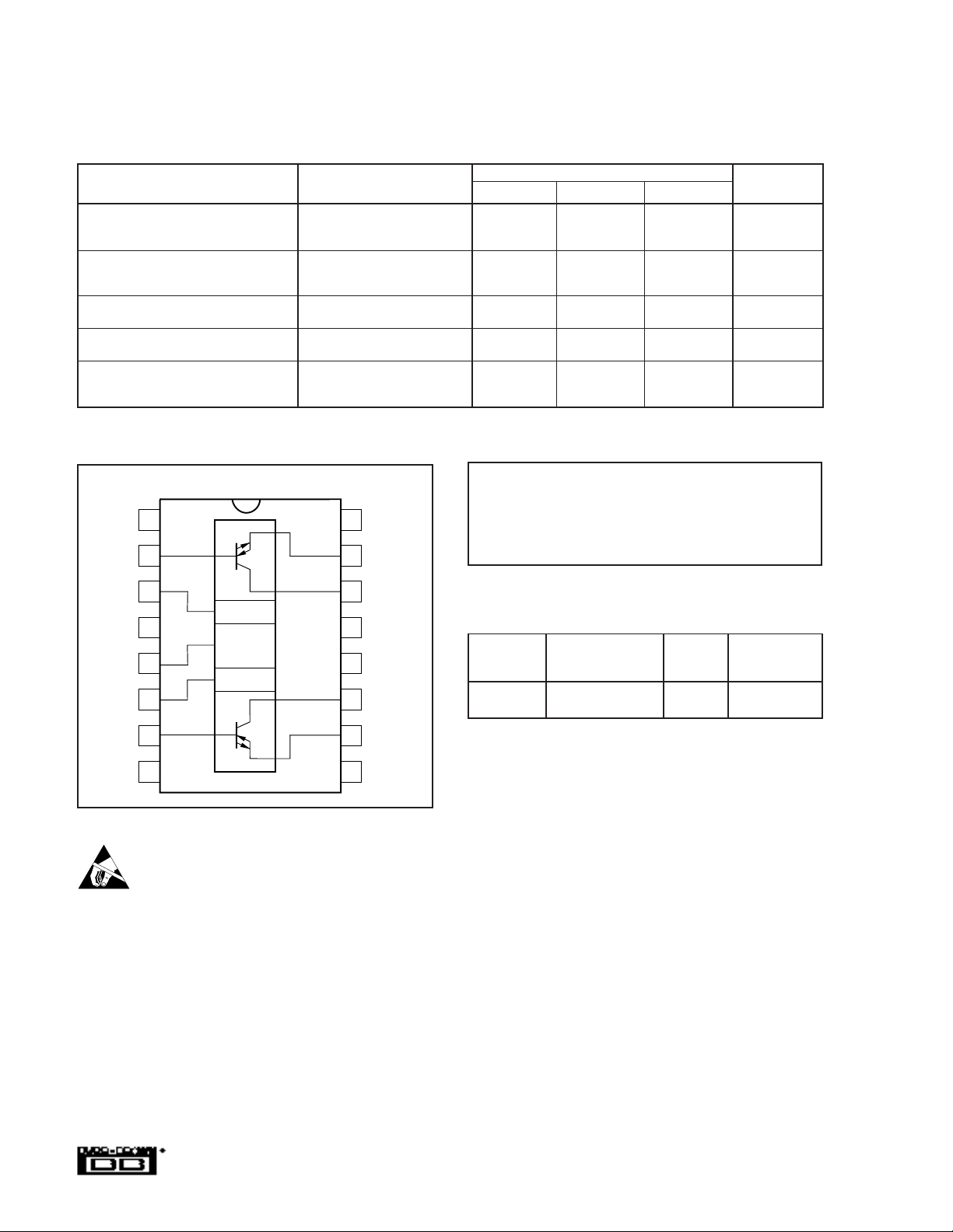
PIN CONFIGURATION
Top View SOL-16/DIP
+V
1
CC
B
2
1
OTA1
Logic
PTAT
Supply
Logic
OTA2
I
Adjust
Q
EN
GND
EN
3
1
4
5
6
2
B
7
2
°C to +85°C)
OPA2662AP, AU
= 50kΩ, RC = 40Ω
E
= 100Ω, RC = 40Ω
E
= 75mA, RE = 0 580 610 mA/V
C
ABSOLUTE MAXIMUM RATINGS
Power Supply Voltage ........................................................................ ±6V
Input Voltage
Operating Temperature ................................................... –40°C to +85°C
16
+V
CCOUT
15
E
1
14
C
1
13
NC
12
NC
11
C
2
10
E
2
Storage Temperature ..................................................... –40°C to +125°C
Junction Temperature .................................................................... +175°C
Lead Temperature (soldering, 10s) ............................................... +300°C
Digital Input Voltages (EN
NOTE: (1) Inputs are internally diode-clamped to ±VCC.
PACKAGE/ORDERING INFORMATION
PRODUCT PACKAGE NUMBER
OPA2662AP 16-Pin Plastic DIP 180 –40°C to +85°C
OPA2662AU SOL-16 Surface Mount 211 –40°C to +85°C
NOTE: (1) For detailed drawing and dimension table, please see end of data
sheet, or Appendix C of Burr-Brown IC Data Book.
(1)
.................................................................. ±VCC to ±0.7V
, EN2) ............................... –0.5 to +VCC +0.7V
1
PACKAGE
DRAWING TEMPERATURE
(1)
RANGE
–V
8
CC
OPA2662
9
–V
CCOUT
ELECTROSTATIC
DISCHARGE SENSITIVITY
Any integrated circuit can be damaged by ESD. Burr-Brown
recommends that all integrated circuits be handled with appropriate precautions. ESD can cause damage ranging from
subtle performance degradation to complete device failure.
Precision integrated circuits may be more susceptible to
damage because very small parametric changes could cause
the device not to meet published specifications.
Burr-Brown’s standard ESD test method consists of five
1000V positive and negative discharges (100pF in series with
1.5kΩ) applied to each pin.
OPA2662
4
TYPICAL PERFORMANCE CURVES
At VCC = ±5V, RQ = 750Ω, and TA = +25°C, unless otherwise specified.
OTA B TO E-INPUT OFFSET VOLTAGE
15
14
13
12
11
10
Input Offset Voltage (mV)
9
8
–50 –25 0 25 50 75 100
vs TEMPERATURE
RE = 50kΩ
R
Temperature (°C)
OTA C-OUTPUT BIAS CURRENT vs TEMPERAURE
0.70
0.65
0.60
0.55
0.50
0.45
0.40
Output Bias Current (mA)
0.35
0.30
–50 –25 0 25 50 75 100
Temperature (°C)
= 40Ω
C
OTA B-INPUT RESISTANCE
18
16
14
12
10
8
6
4
OTA B-Input Resistance (MΩ)
2
0
7 12 17 22 27 32 37 42 47
vs TOTAL QUIESCENT CURRENT
Total Quiescent Current, I
(±mA)
Q
OTA B-INPUT BIAS CURRENT vs TEMPERATURE
1.5
1.3
1.1
0.9
B-Input Bias Current (µA)
0.7
–50 –25 0 25 50 75 100
Temperature (C°)
OTA E-OUTPUT RESISTANCE
50
45
(Ω)
40
E
35
30
25
20
15
10
OTA E-Output Resistance r
5
0
747
vs TOTAL QUIESCENT CURRENT
3212 17 22 27 37 42
Total Quiescent Current, I
Q
(±mA)
9
8
(kΩ)
C
7
6
5
4
3
2
1
OTA C-Output Resistance, r
0
7 12 17 22 27 32 37 42 47
OTA C-OUTPUT RESISTANCE
vs TOTAL QUIESCENT CURRENT
Total Quiescent Current, I
5 OPA2662
(±mA)
Q
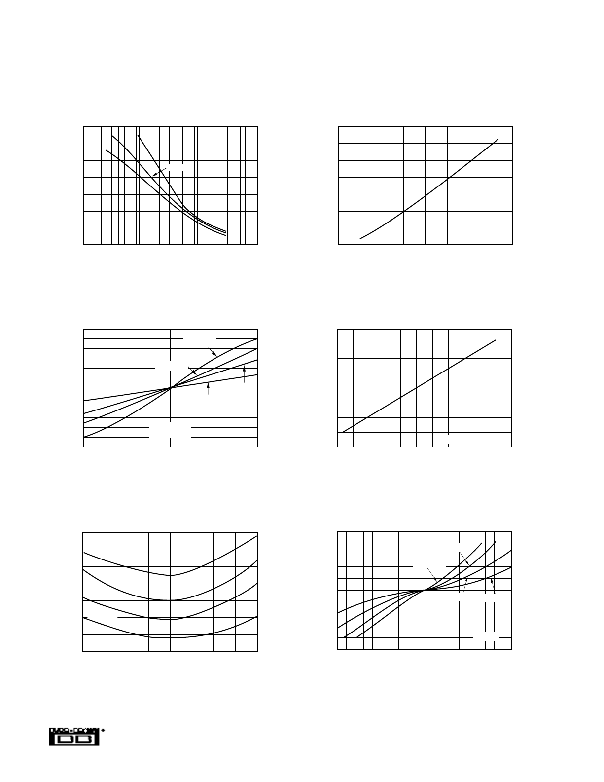
TYPICAL PERFORMANCE CURVES (CONT)
At VCC = ±5V, RQ = 750Ω, and TA = +25°C, unless otherwise specified.
70
60
(±mA)
Q
50
40
30
20
10
Total Quiescent Current, I
0
10
120
80
40
0
–40
OTA C-Output Current (mA)
–80
–120
–0.95
TOTAL QUIESCENT CURRENT vs R
OTA TRANSFER CHARACTERISTICS vs R
Q
Typical
100 1k 10k
RQ - Resistor Value (Ω)
E
RE = 25Ω
RE = 33Ω
RE = 50Ω
RE = 100Ω
RC = 10Ω
= 1.9Vp-p
V
IN
0 0.95
Input Voltage (V)
QUIESCENT CURRENT CHANGE vs TEMPERATURE
24
22
20
18
16
14
Quiescent Current (mA)
12
10
–60 –40 –20 0 20 40 8060
Temperature (°C)
100
75
50
25
0
–25
–50
OTA C-Output Current (mA)
–75
–100
–25
–20 –15 –10 –5 0 5 10 15 20 25 30
IC/IE TRANSFER CURVE
OTA E-Output Current (mA)
100
RE = 33Ω, RC = 11Ω
700
600
500
400
300
200
100
OTA Transconductance gm (mA/V)
0
–200 –150 –100 –50 0 50 100 150 200
TRANSCONDUCTANCE vs VIN vs I
I
= 65mA
Q
I
= 34mA
Q
IQ = 17mA
I
= 8mA
Q
Input Voltage (mV)
OPA2662
OTA TRANSFER CHARACTERISTICS
Q
100
80
60
40
20
0
–20
–40
–60
OTA C-Output Current (mA)
–80
–100
–200 –100 0 100 200
vs TOTAL QUIESCENT CURRENT
IQ = ±34mA
IQ = ±65mA
IQ = ±17mA
Input Voltage (mV)
IQ = ±8mA
RE = 0Ω
6
 Loading...