

Burr Brown OPA2652U, OPA2652U-2K5, OPA2652E-3K, OPA2652E Datasheet
FEATURES
● WIDEBAND BUFFER: 700MHz, G = +1
● WIDEBAND LINE DRIVER: 200MHz, G = +2
● HIGH OUTPUT CURRENT: 140mA
● LOW SUPPLY CURRENT: 5.5mA/Ch
● ULTRA-SMALL PACKAGE: SOT23-8
● LOW dG/dφ: 0.05%/0.03°
● HIGH SLEW RATE: 335V/µsec
● SUPPLY VOLTAGE: ±3V to ±6V
DESCRIPTION
The OPA2652 is a dual, low-cost, wideband voltagefeedback amplifier intended for price sensitive applications. It features a high gain bandwidth product of 200MHz
on only 5.5mA/chan quiescent current. Intended for operation on ±5V supplies, it will also support applications
on a single supply from +6V to +12V with 140mA output
current. Its classical differential input, voltage-feedback
design allows wide application in active filters, integrators, transimpedance amplifiers, and differential receivers.
The OPA2652 is internally compensated for unity gain
stability. It has exceptional bandwidth (700MHz) as a unity
gain buffer, with little peaking (0dB typically). Excellent
DC accuracy is achieved with a low 1.5mV input offset
voltage and 300nA input offset current.
Dual, 700MHz, Voltage-Feedback
OPERATIONAL AMPLIFIER
APPLICATIONS
● A/D DRIVERS
● CONSUMER VIDEO
● ACTIVE FILTERS
● PULSE DELAY CIRCUITS
● LOW COST UPGRADE TO THE AD8056
OR EL2210
®
OPA2652
TM
RELATED PRODUCTS
SINGLES DUALS TRIPLES QUADS NOTES
OPA650 OPA2650 — OPA4650 ±5V Spec
OPA680 OPA2680 OPA3680 — +5V Capable
OPA631 OPA2631 — — +3V Capable
OPA634 OPA2634 — — +3V Capable
International Airport Industrial Park • Mailing Address: PO Box 11400, Tucson, AZ 85734 • Street Address: 6730 S. Tucson Blvd., Tucson, AZ 85706 • Tel: (520) 746-1111
Twx: 910-952-1111 • Internet: http://www.burr-brown.com/ • Cable: BBRCORP • Telex: 066-6491 • FAX: (520) 889-1510 • Immediate Product Info: (800) 548-6132
For most current data sheet and other product
information, visit www.burr-brown.com
© 2000 Burr-Brown Corporation PDS-1588B Printed in U.S.A. June, 2000
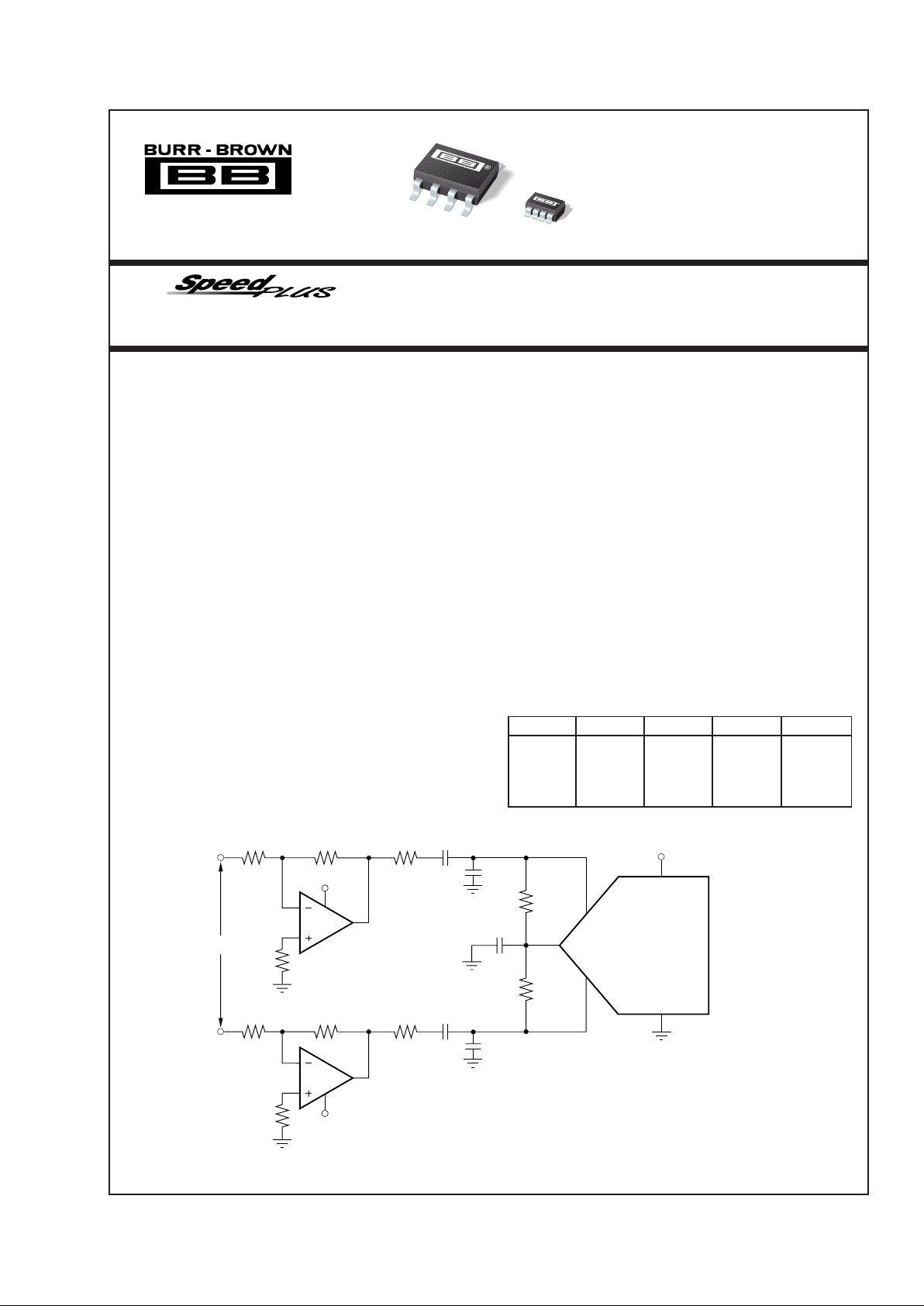
OPA2652
Differential ADC Driver
ADS807
12-Bit
53MHz
+In
CM
–In
+5V
402Ω
+5V
24.9Ω
133Ω
V
IN
200Ω
1/2
OPA2652
1/2
OPA2652
22pF
1.00kΩ
0.1µF
–5V
402Ω
24.9Ω
133Ω
200Ω
–
+
22pF
0.1µF
0.1µF
1.00kΩ

2
®
OPA2652
OPA2652U, E
TYP GUARANTEED
0°C to –40°C to
MIN/
TEST
PARAMETER CONDITIONS +25°C +25°C
(2)
70°C
(3)
+85°C
(3)
UNITS MAX
LEVEL
(1)
SPECIFICATIONS: VS = ±5V
At TA = +25°C, G = +2, RF = 402Ω, and RL = 100Ω, unless otherwise noted. See Figures 1 and 2 for AC performance only.
AC PERFORMANCE
(Figures 1 and 2)
Small-Signal Bandwidth G = +1, R
F
= 25Ω, VO = 200mVp-p 700 MHz typ C
G = +2, V
O
= 200mVp-p 200 MHz typ C
G = +5, V
O
= 200mVp-p 45 MHz typ C
Gain Bandwidth Product G ≥ +10 200 MHz typ C
Bandwidth for 0.1dB Flatness V
O
= 200mVp-p 50 MHz typ C
Peaking at a Gain of +1 G = +1, R
F
= 25Ω,VO = 200mVp-p 0 dB typ C
Slew Rate 4V Step 335 V/µs typ C
Rise/Fall Time 200mV Step 2.0 ns typ C
4V Step 10 ns typ C
Large Signal Bandwidth V
O
= 4Vp-p 50 MHz typ C
SFDR V
O
= 2Vp-p, 5MHz 66 dB typ C
Input Voltage Noise f > 1MHz 8 nV/√Hz typ C
Input Current Noise f > 1MHz 1.4 pA/√Hz typ C
Differential Gain Error NTSC, R
L
= 150Ω 0.05 % typ C
Differential Phase Error NTSC, R
L
= 150Ω 0.03 degrees typ C
Channel-to-Channel Crosstalk f = 5MHz –100 dBc typ C
DC PERFORMANCE
(4)
VCM = 0V
Open-Loop Voltage Gain 63 56 55 54 dB min A
Input Offset Voltage ±1.5 ±7 mV max A
Average Offset Drift 57µV/°C max B
Input Bias Current 4 152025µA max A
Input Bias Current Drift µA/°C max B
Input Offset Current ±0.3 ±1.0 ±1.4 ±2.0 µA max A
Input Offset Current Drift µA/°C max B
INPUT
(4)
Common-Mode Input Range ±4.0 ±3.0 ±2.8 ±2.7 V min A
Common-Mode Rejection Ratio 95 75 dB min A
Input Impedance V
CM
= 0V
Differential 35 || 1 kΩ || pF typ C
Common Mode 18 || 1 MΩ || pF typ C
OUTPUT
Voltage Output Swing 1kΩ Load ±3.0 ±2.4 V min A
100Ω Load ±2.5 ±2.2 V min A
Output Current, Sourcing V
O
= 0V 140 100 85 75 mA min A
Output Current, Sinking V
O
= 0V 140 100 85 75 mA min A
Closed-Loop Output Impedance f < 100kHz 0.06 Ω typ C
POWER SUPPLY
Specified Operating Voltage ±5 V typ C
Maximum Operating Voltage ±6 ±6 ±6 V max A
Maximum Quiescent Current Total Both Channels 11 13.2 14 15.5 mA max A
Minimum Quiescent Current Total Both Channels 11 8.8 8 7.5 mA min A
Power Supply Rejection Ratio (–PSRR) Input Referred 58 54 dB min A
THERMAL CHARACTERISTICS
Specified Operating Temperature Range U, E Package
–40 to +85
°C typ C
Thermal Resistance,
θ
JA
Junction-to-Ambient
U SO-8 125 °C/W typ C
E SOT23-8 150 °C/W typ C
NOTES: (1) Test Levels: (A) 100% tested at 25°C. Over temperature limits by characterization and simulation. (B) Limits set by characterization and simulation.
(C) Typical value only for information. (2) Junction temperature = ambient for 25°C guaranteed specifications. (3) Junction temperature = ambient at low temperature
limit: junction temperature = ambient +23°C at high temperature limit for over temperature guaranteed specifications. (4) Current is considered positive-out-of node.
V
CM
is the input common-mode voltage.
3
®
OPA2652
Supply Voltage ................................................................................. ±6.5V
Internal Power Dissipation ........................... See Thermal Characteristics
Differential Input Voltage .................................................................. ±1.2V
Input Voltage Range ............................................................................ ±V
S
Storage Temperature Range ......................................... –40 °C to +125°C
Lead Temperature (SO-8) ............................................................. +260°C
Junction Temperature (T
J
) ........................................................... +175°C
ESD Rating (Human Body Model) .................................................. 2000V
(Machine Model) ........................................................... 200V
The information provided herein is believed to be reliable; however, BURR-BROWN assumes no responsibility for inaccuracies or omissions. BURR-BROWN assumes no responsibility for the use
of this information, and all use of such information shall be entirely at the user’s own risk. Prices and specifications are subject to change without notice. No patent rights or licenses to any of the
circuits described herein are implied or granted to any third party. BURR-BROWN does not authorize or warrant any BURR-BROWN product for use in life support devices and/or systems.
ELECTROSTATIC
DISCHARGE SENSITIVITY
Electrostatic discharge can cause damage ranging from performance degradation to complete device failure. Burr-Brown
Corporation recommends that all integrated circuits be handled
and stored using appropriate ESD protection methods.
ESD damage can range from subtle performance degradation
to complete device failure. Precision integrated circuits may
be more susceptible to damage because very small parametric
changes could cause the device not to meet published specifications.
ABSOLUTE MAXIMUM RATINGS
Top View SO-8
SOT23-8
PIN CONFIGURATION
PACKAGE/ORDERING INFORMATION
PACKAGE SPECIFIED
DRAWING TEMPERATURE PACKAGE ORDERING TRANSPORT
PRODUCT PACKAGE NUMBER RANGE MARKING NUMBER
(1)
MEDIA
OPA2652U SO-8 Surface Mount 182 –40°C to +85°C OPA2652U OPA2652U Rails
" " """OPA2652U/2K5 Tape and Reel
OPA2652E SOT23-8 Surface Mount 348 –40°C to +85°C C52 OPA2652E/250 Tape and Reel
" " """OPA2652E/3K Tape and Reel
NOTE: (1) Models with a slash (/) are available only in Tape and Reel in the quantities indicated (e.g., /3K indicates 3000 devices per reel). Ordering 3000 pieces of
“OPA2652U/3K” will get a single 3000-piece Tape and Reel.
1
2
3
4
8
7
6
5
+V
S
Out B
–In B
+In B
Out A
–In A
+In A
–V
S
OPA2652
C52
Pin 1
SOT23-8 Marking/Pin Orientation
4
®
OPA2652
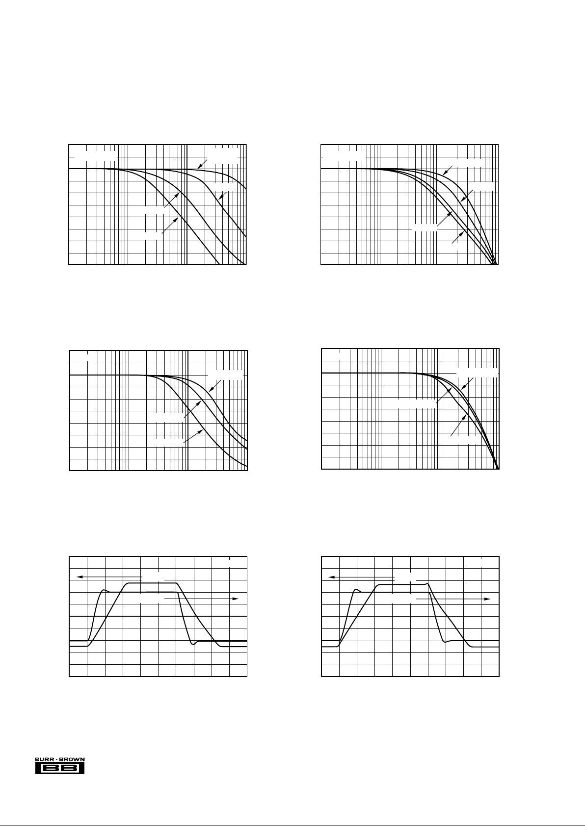
TYPICAL PERFORMANCE CURVES: VS = ±5V
At TA = +25°C, G = +2, RF = 402Ω, and RL = 100Ω, unless otherwise noted. See Figures 1 and 2.
6
3
0
–3
–6
–9
–12
–15
–18
–21
–24
NON-INVERTING
SMALL-SIGNAL FREQUENCY RESPONSE
Frequency (Hz)
Normalized Gain (dB)
1M 10M 100M 1G
VO = 0.2Vp-p
G = +5
G = +10
G = +1
R
F
= 25Ω
G = +2
6
3
0
–3
–6
–9
–12
–15
–18
–21
–24
INVERTING
LARGE-SIGNAL FREQUENCY RESPONSE
Frequency (Hz)
Normalized Gain (dB)
1M 10M 100M 1G
VO = 0.5Vp-p
G = –1
VO = 1.0Vp-p
VO = 2.0Vp-p
NON-INVERTING PULSE RESPONSE
Time (5ns/div)
Output Voltage (800mV/div)
Output Voltage (50mV/div)
4Vp-p
G = +2
200mVp-p
INVERTING PULSE RESPONSE
Time (5ns/div)
Output Voltage (800mV/div)
Output Voltage (50mV/div)
4Vp-p
G = –1
200mVp-p
6
3
0
–3
–6
–9
–12
–15
–18
–21
–24
NON-INVERTING
LARGE-SIGNAL FREQUENCY RESPONSE
Frequency (Hz)
Normalized Gain (dB)
1M 10M 100M 1G
VO ≤ 1Vp-p
G = +2
VO = 2Vp-p
VO = 4Vp-p
6
3
0
–3
–6
–9
–12
–15
–18
–21
–24
INVERTING
SMALL-SIGNAL FREQUENCY RESPONSE
Frequency (Hz)
Normalized Gain (dB)
1M 10M 100M 1G
VO = 0.2Vp-p
G = –5
G = –10
G = –1
G = –2
5
®
OPA2652
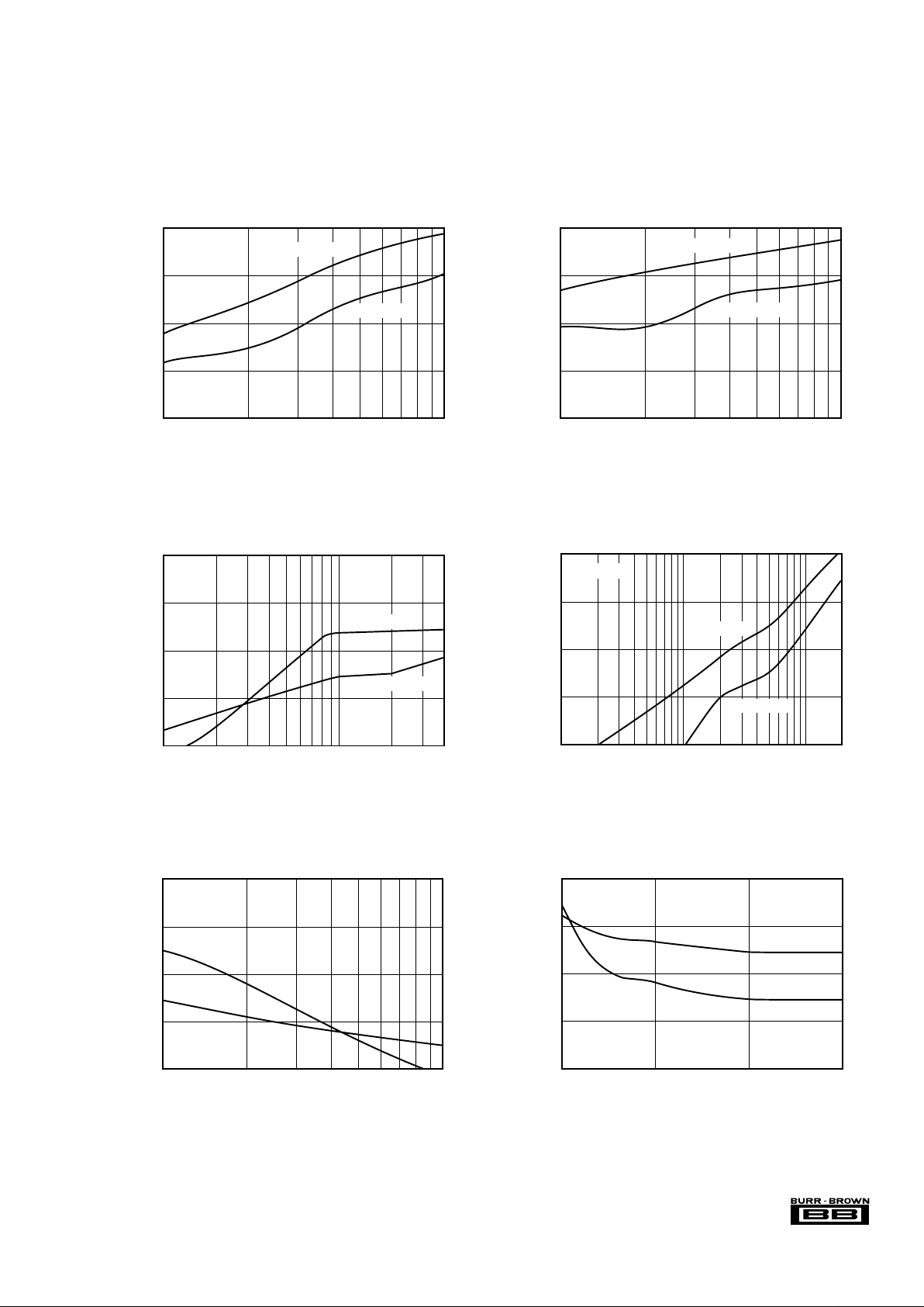
TYPICAL PERFORMANCE CURVES: VS = ±5V (Cont.)
At TA = +25°C, G = +2, RF = 402Ω, and RL = 100Ω, unless otherwise noted. See Figures 1 and 2.
–50
–60
–70
–80
–90
HARMONIC DISTORTION vs FREQUENCY
Frequency (MHz)
0.1 1 10 20
Harmonic Distortion (dBc)
VO = 2Vp-p
3rd Harmonic
2nd Harmonic
–50
–60
–70
–80
–90
HARMONIC DISTORTION vs LOAD RESISTANCE
R
L
(Ω)
100 1000
Harmonic Distortion (dBc)
VO = 2Vp-p
f = 5MHz
3rd Harmonic
2nd Harmonic
–50
–60
–70
–80
–90
HARMONIC DISTORTION vs SUPPLY VOLTAGE
Supply Voltage (V)
±3 ±4 ±5 ±6
Harmonic Distortion (dBc)
VO = 2Vp-p
f
= 5MHz
3rd Harmonic
2nd Harmonic
–50
–60
–70
–80
–90
HARMONIC DISTORTION vs NON-INVERTING GAIN
Gain Magnitude (V/V)
Harmonic Distortion (dBc)
110
V
O
= 2Vp-p
f = 5MHz
2nd Harmonic
3rd Harmonic
–50
–60
–70
–80
–90
HARMONIC DISTORTION vs INVERTING GAIN
Gain Magnitude (V/V)
Harmonic Distortion (dBc)
110
V
O
= 2Vp-p
f = 5MHz
2nd Harmonic
3rd Harmonic
–50
–60
–70
–80
–90
HARMONIC DISTORTION vs OUTPUT VOLTAGE
Output Voltage (Vp-p)
Harmonic Distortion (dBc)
0.1 1 4
f = 5MHz
3rd Harmonic
2nd Harmonic
 Loading...