

Page 1
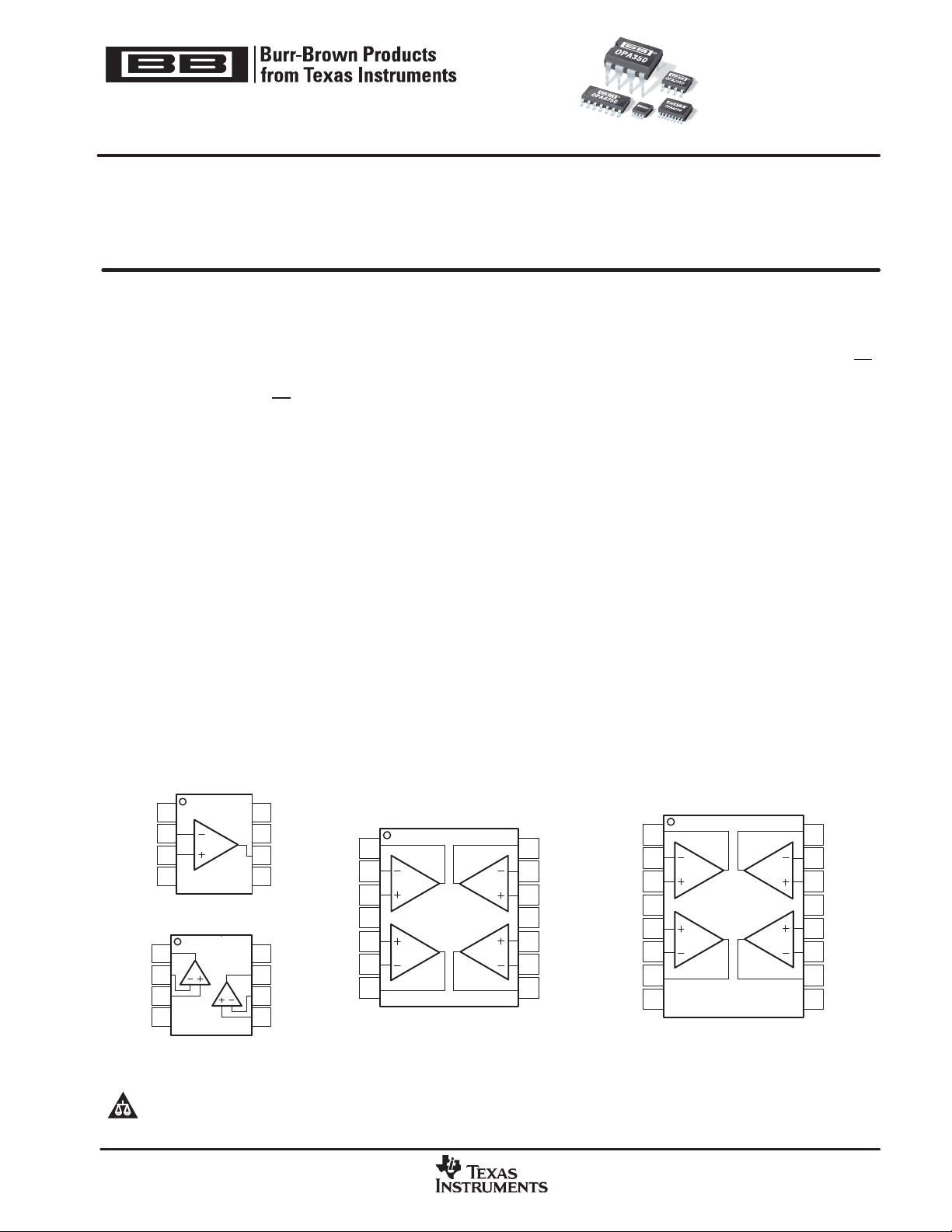
OPA2350
Please be aware that an important notice concerning availability, standard warranty, and use in critical applications of Texas Instruments
OPA4350
SBOS099C − SEPTEMBER 2000 − REVISED JANUARY 2005
High-Speed, Single-Supply, Rail-to-Rail
OPERATIONAL AMPLIFIERS
MicroAmplifiertSeries
OPA350
FEATURES
D RAIL-TO-RAIL INPUT
D RAIL-TO-RAIL OUTPUT (within 10mV)
D WIDE BANDWIDTH: 38MHz
D HIGH SLEW RATE: 22V/µs
D LOW NOISE: 5nV/√Hz
D LOW THD+NOISE: 0.0006%
D UNITY-GAIN STABLE
D MicroSIZE PACKAGES
D SINGLE, DUAL, AND QUAD
APPLICATIONS
D CELL PHONE PA CONTROL LOOPS
D DRIVING A/D CONVERTERS
D VIDEO PROCESSING
D DATA ACQUISITION
D PROCESS CONTROL
D AUDIO PROCESSING
D COMMUNICATIONS
D ACTIVE FILTERS
D TEST EQUIPMENT
DESCRIPTION
The OPA350 series rail-to-rail CMOS operational
amplifiers are optimized for low voltage, single-supply
operation. Rail-to-rail input/output, low noise (5nV/√Hz
and high speed operation (38MHz, 22V/µs) make them
ideal for driving sampling Analog-to-Digital (A/D)
converters. They are also well suited for cell phone PA
control loops and video processing (75Ω drive capability)
as well as audio and general purpose applications. Single,
dual, and quad versions have identical specifications for
maximum design flexibility.
The OPA350 series operates on a single supply as low as
2.5V with an input common-mode voltage range that
extends 300mV below ground and 300mV above the
positive supply. Output voltage swing is to within 10mV of
the supply rails with a 10kΩ load. Dual and quad designs
feature completely independent circuitry for lowest
crosstalk and freedom from interaction.
The single (OPA350) and dual (OPA2350) come in the
miniature MSOP-8 surface mount, SO-8 surface mount,
and DIP-8 packages. The quad (OPA4350) packages are
the space-saving SSOP-16 surface mount and SO-14
surface mount. All a r e s p e c i f i e d f r o m − 4 0 °C to +85°C and
operate from −55°C to +150°C.
),
OPA350
1
NC
2
−In
3
+In
−
4
V
DIP−8, SO−8, MSOP−8
OPA2350
1
OutA
A
2
−In A
3
+In A
−
4
DIP−8, SO−8, MSOP−8
semiconductor products and disclaimers thereto appears at the end of this data sheet.
All trademarks are the property of their respective owners.
! !
B
NC
8
V+
7
Output
6
NC
5
8
V+
7
Out B
6
−In B
5
+In B
Out A
−In A
+In A
V+
+In B
−In B
Out B
1
2
3
4
5
6
7
OPA4350
AD
BC
SO−14
SPICE model available at www.ti.com
Out A
−In A
+In A
+V
+In B
−In B
Out B
NC
Copyright 2000−2005, Texas Instruments Incorporated
www.ti.com
14
Out D
13
−In D
12
+In D
11
V
−
10
+In C
9
−In C
8
Out C
OPA4350
1
2
AD
3
4
5
BC
6
7
8
SSOP−16
16
Out D
15
−In D
14
+In D
−
13
V
12
+In C
11
−In C
10
Out C
9
NC
Page 2
"#$
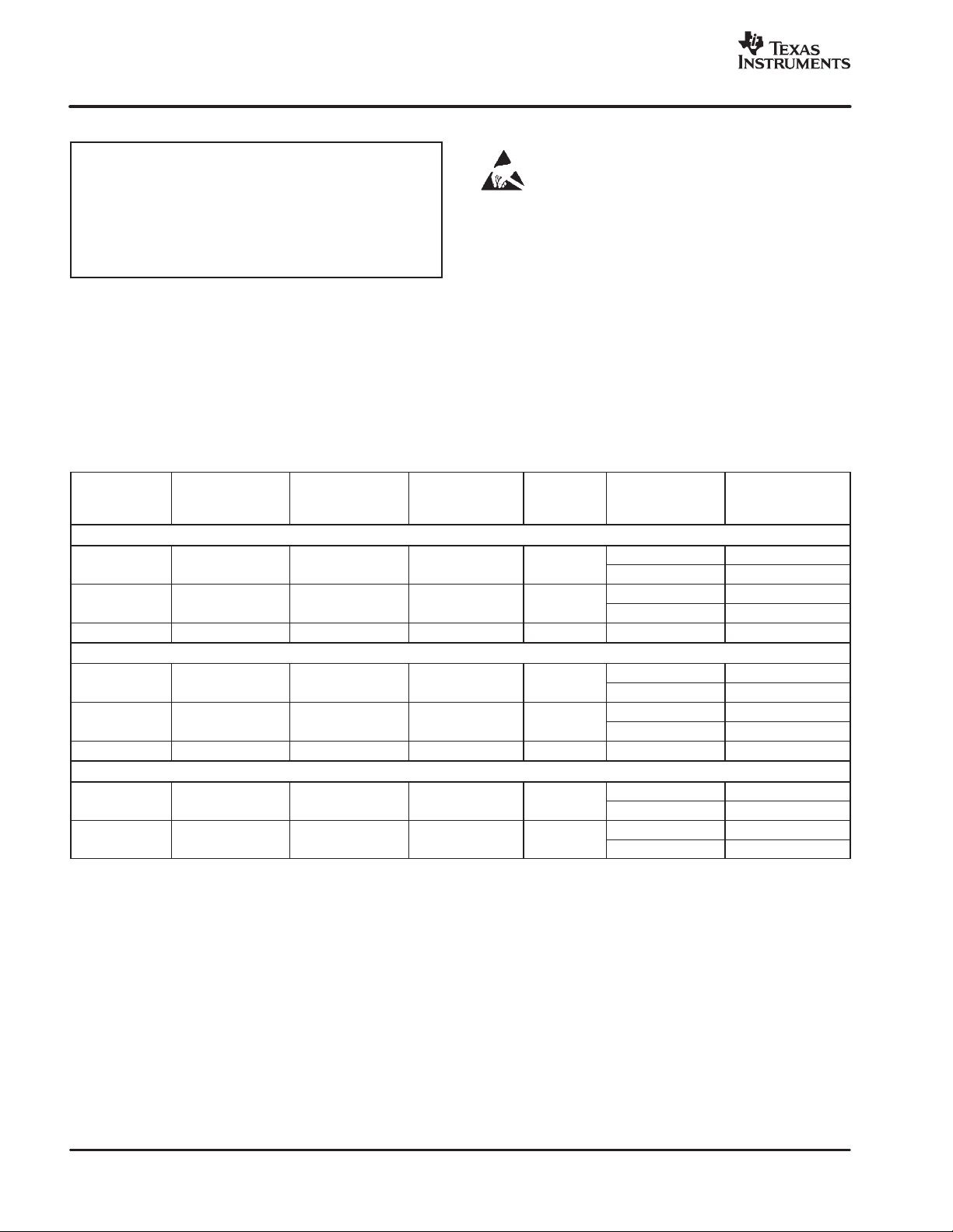
OPA350EA
MSOP-8
DGK
−40°C to +85°C
C50
OPA350UA
SO-8
D
−40°C to +85°C
OPA350UA
OPA2350EA
MSOP-8
DGK
−40°C to +85°C
D50
OPA2350UA
SO-8
D
−40°C to +85°C
OPA2350UA
OPA4350EA
SSOP-16
DBQ
−40°C to +85°C
OPA4350EA
OPA4350UA
SO-14
D
−40°C to +85°C
OPA4350UA
%"#$
&"#$
SBOS099C − SEPTEMBER 2000 − REVISED JANUARY 2005
www.ti.com
ABSOLUTE MAXIMUM RATINGS
Supply Voltage 7.0V. . . . . . . . . . . . . . . . . . . . . . . . . . . . . . . . . . . . . .
Signal Input Terminals
Open Short-Circuit Current
Operating Temperature Range −55°C to +150°C. . . . . . . . . . . . . . .
Storage Temperature Range −55°C to +150°C. . . . . . . . . . . . . . . . .
Junction Temperature +150°C. . . . . . . . . . . . . . . . . . . . . . . . . . . . . . .
Lead Tem perature (soldering, 10s) +300°C. . . . . . . . . . . . . . . . . . . . .
(1)
Stresses above these ratings may cause permanent damage.
Exposure to absolute maximum conditions for extended periods
may degrade device reliability. These are stress ratings only , an d
functional operation of the device at these or any other conditions
beyond those specified is not implied.
(2)
Input terminals are diode-clamped to the power-supply rails.
Input signals that can swing more than 0.3V beyond the supply
rails should be current limited to 10mA or less.
(3)
Short-circuit to ground, one amplifier per package.
(2)
,Voltage (V−) − 0.3V to (V+) + 0.3V. . . . .
Current 10mA. . . . . . . . . . . . . . . . . . . . . .
(3)
PACKAGE/ORDERING INFORMATION
PRODUCT PACKAGE-LEAD
SINGLE
OPA350PA DIP-8 P −40°C to +85°C OPA350PA OPA350PA Rails
DUAL
OPA2350PA DIP-8 P −40°C to +85°C OPA2350PA OPA2350PA Rails
QUAD
(1)
For the most current package and ordering information, see the Package Option Addendum located at the end of this data sheet.
(1)
Continuous. . . . . . . . . . . . . . . . . . . .
PACKAGE
DESIGNATOR
(1)
TEMPERATURE
ELECTROSTATIC DISCHARGE SENSITIVITY
This integrated circuit can be damaged by ESD. Texas
Instruments recommends that all integrated circuits be
handled with appropriate precautions. Failure to observe
proper handling and installation procedures can cause damage.
ESD damage can range from subtle performance degradation to
complete device failure. Precision integrated circuits may be more
susceptible t o damage because very small parametric changes could
cause the device not to meet its published specifications.
SPECIFIED
RANGE
PACKAGE
MARKING
ORDERING
NUMBER
OPA350EA/250 Tape and Reel, 250
OPA350EA/2K5 Tape and Reel, 2500
OPA350UA Rails
OPA350UA/2K5 Tape and Reel, 2500
OPA2350EA/250 Tape and Reel, 250
OPA2350EA/2K5 Tape and Reel, 2500
OPA2350UA Rails
OPA2350UA/2K5 Tape and Reel, 2500
OPA4350EA/250 Tape and Reel, 250
OPA4350EA/2K5 Tape and Reel, 2500
OPA4350UA Rails
OPA4350UA/2K5 Tape and Reel, 2500
MEDIA, QUANTITY
TRANSPORT
2
Page 3
"#$
%"#$
www.ti.com
SBOS099C − SEPTEMBER 2000 − REVISED JANUARY 2005
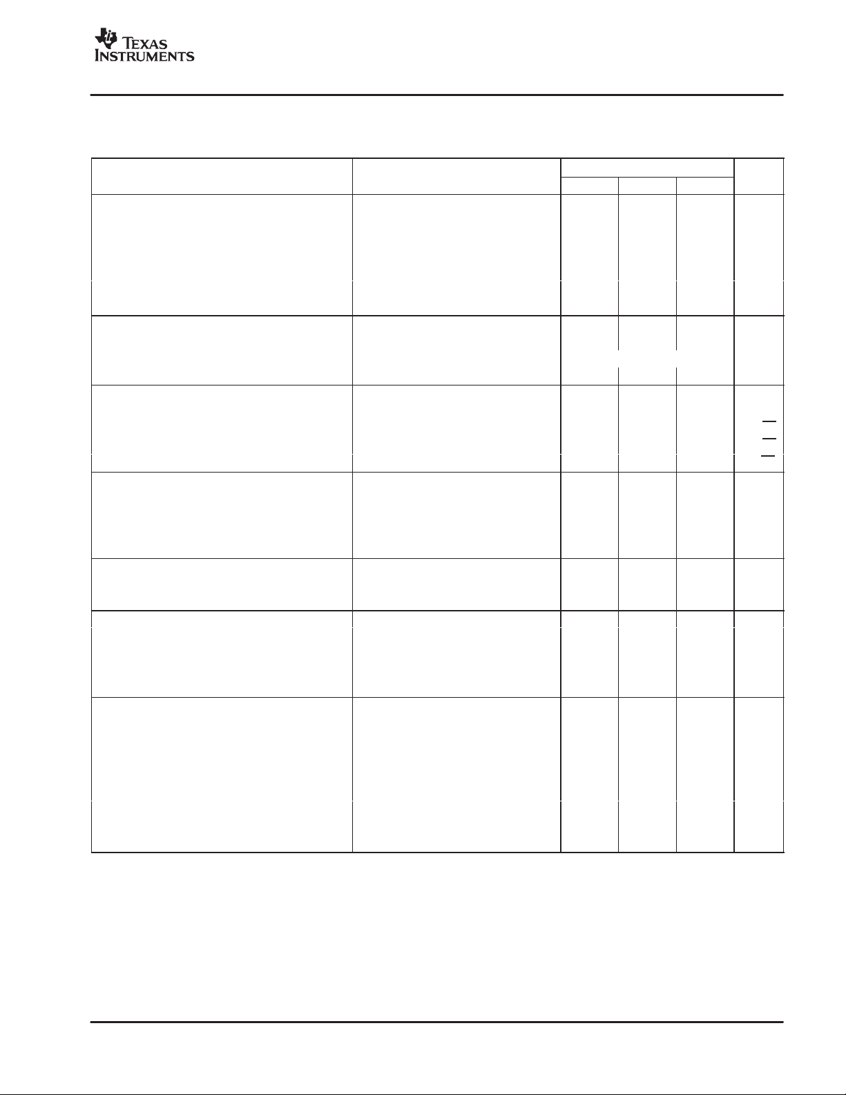
ELECTRICAL CHARACTERISTICS: VS = 2.7V to 5.5V
Boldface limits apply over the temperature range, TA = −40°C to +85°C. VS = 5V.
All specifications at TA = +25°C, RL = 1kΩ connected to VS/2 and V
PARAMETER TEST CONDITIONS MIN TYP
OFFSET VOLTAGE
Input Offset Voltage V
TA = −40°C to +85°C ±1 mV
vs Temperature TA = −40°C to +85°C ±4 µV/°C
vs Power-Supply Rejection Ratio PSRR VS = 2.7V to 5.5V , VCM = 0V 40 150 µV/V
TA = −40°C to +85°C VS = 2.7V to 5.5V , VCM = 0V 175 µV/V
Channel Separation (dual, quad) dc 0.15 µV/V
INPUT BIAS CURRENT
Input Bias Current I
vs Temperature See Typical Characteristics
Input Offset Current I
NOISE
Input Voltage Noise, f = 100Hz to 400kHz 4 µVrms
Input Voltage Noise Density, f = 10kHz e
Input Current Noise Density, f = 100kHz 5 nV/√Hz
Current Noise Density, f = 10kHz i
INPUT VOLTAGE RANGE
Common-Mode Voltage Range V
Common-Mode Rejection Ratio CMRR VS = 2.7V , −0.1V < VCM < 2.8V 66 84 dB
TA = −40°C to +85°C VS = 5.5 V, −0.1V < VCM < 5.6V 74 dB
INPUT IMPEDANCE
Differential 1013 || 2.5 Ω || pF
Common-Mode 1013 || 6.5 Ω || pF
OPEN-LOOP GAIN
Open-Loop Voltage Gain A
TA = −40°C to +85°C RL = 10kW, 50mV < VO < (V+) −50mV 100 dB
TA = −40°C to +85°C RL = 1kW, 200mV < VO < (V+) −200mV 100 dB
FREQUENCY RESPONSE CL = 100pF
Gain-Bandwidth Product GBW G = 1 38 MHz
Slew Rate SR G = 1 22 V/µs
Settling Time: 0.1% G = ±1, 2V Step 0.22 µs
0.01% G = ±1, 2V Step 0.5 µs
Overload Recovery Time VIN • G = V
Total Harmonic Distortion + Noise THD+N RL = 600Ω, VO = 2.5V
Differential Gain Error G = 2, RL = 600Ω, VO = 1.4V
Differential Phase Error G = 2, RL = 600Ω, VO = 1.4V
(1)
VS = +5V .
(2)
V
= 0.25V to 2.75V .
OUT
(3)
NTSC signal generator used. See Figure 6 for test circuit.
(4)
Output voltage swings are measured between the output and power supply rails.
(5)
See typical characteristic curve, Output Voltage Swing vs Output Current.
OS
B
OS
n
n
CM
VS = 5.5V , −0.1V < VCM < 5.6V 74 90 dB
OLRL
= 10kΩ, 50mV < VO < (V+) −50mV 100 122 dB
RL = 1kΩ, 200mV < VO < (V+) −200mV 100 120 dB
= VS/2, unless otherwise noted.
OUT
OPA350, OPA2350, OPA4350
(1)
VS = 5V ±150 ±500 µV
±0.5 ±10 pA
±0.5 ±10 pA
7 nV/√Hz
4 fA/√Hz
TA = −40°C to +85°C −0.1 (V+) + 0 .1 V
S
(2)
, G = 1, f = 1kHz 0.0006 %
PP
(3)
(3)
0.1 µs
0.17 %
0.17 deg
&"#$
MAX UNIT
3
Page 4

"#$
%"#$
&"#$
SBOS099C − SEPTEMBER 2000 − REVISED JANUARY 2005
ELECTRICAL CHARACTERISTICS: VS = 2.7V to 5.5V (continued)
Boldface limits apply over the temperature range, TA = −40°C to +85°C. VS = 5V.
All specifications at TA = +25°C, RL = 1kΩ connected to VS/2 and V
PARAMETER UNITMAXTYP
OUTPUT
Voltage Output Swing from Rail
TA = −40°C to +85°C RL = 10kW, AOL 100dB 50 mV
TA = −40°C to +85°C RL = 1kW, AOL 100dB 200 mV
Output Current I
Short-Circuit Current I
Capacitive Load Drive C
POWER SUPPLY
Operating Voltage Range V
Minimum Operating Voltage 2.5 V
Quiescent Current (per amplifier) I
TA = −40°C to +85°C IO = 0 8.5 mA
TEMPERATURE RANGE
Specified Range −40 +85 °C
Operating Range −55 +150 °C
Storage Range −55 +150 °C
Thermal Resistance q
MSOP-8 Surface Mount 150 °C/W
SO-8 Surface Mount 150 °C/W
DIP-8 100 °C/W
SO-14 Surface Mount 100 °C/W
SSOP-16 Surface Mount 100 °C/W
(1)
VS = +5V .
(2)
V
= 0.25V to 2.75V .
OUT
(3)
NTSC signal generator used. See Figure 6 for test circuit.
(4)
Output voltage swings are measured between the output and power supply rails.
(5)
See typical characteristic curve, Output Voltage Swing vs Output Current.
(4)
V
OUT
OUT
SC
LOAD
JA
RL = 10kΩ, AOL ≥ 100dB 10 50 mV
RL = 1kΩ, AOL ≥ 100dB 25 200 mV
S
Q
= VS/2, unless otherwise noted.
OUT
OPA350, OPA2350, OPA4350
MINTEST CONDITIONS
See Typical Characteristics
TA = −40°C to +85°C 2.7 5.5 V
IO = 0 5.2 7.5 mA
(1)
(5)
±40
±80 mA
www.ti.com
mA
4
Page 5
www.ti.com
THD+N (%)
Harmonic Distortion (%)
SBOS099C − SEPTEMBER 2000 − REVISED JANUARY 2005
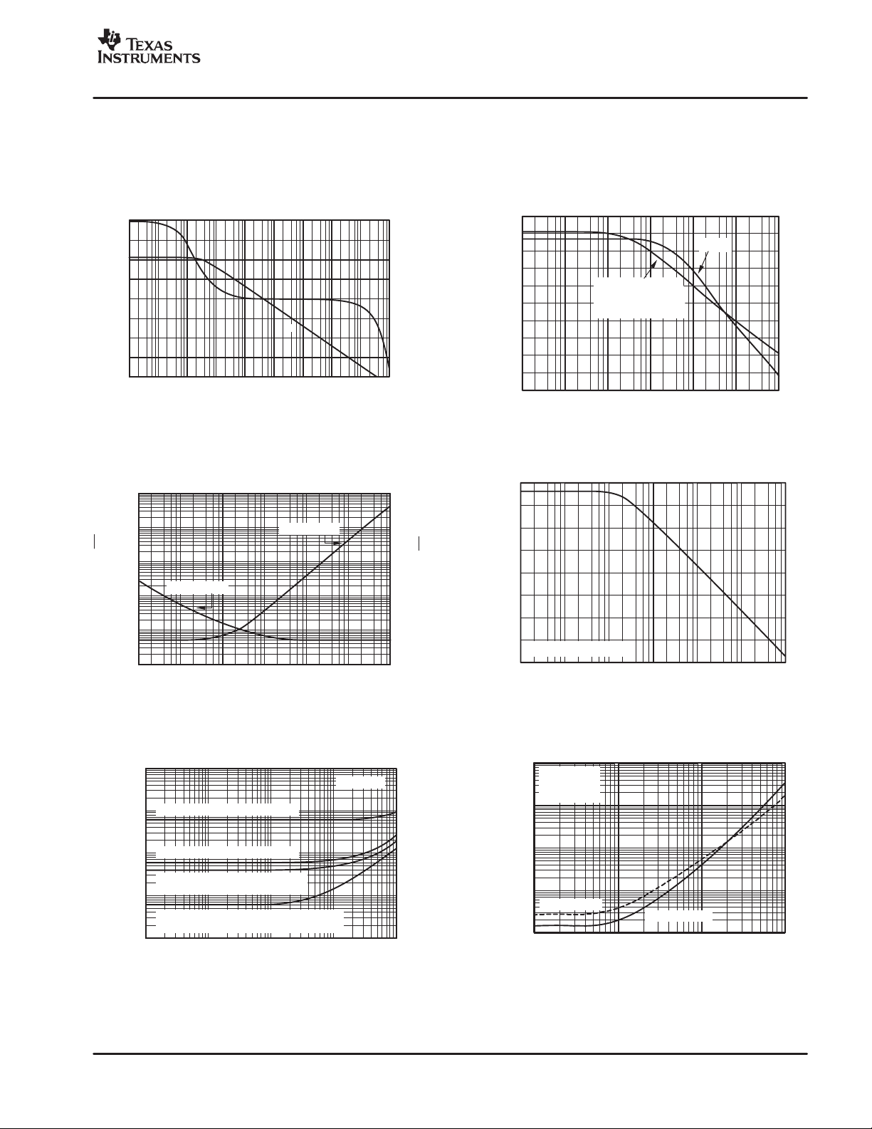
TYPICAL CHARACTERISTICS
All specifications at TA = +25°C, VS = +5V , and RL = 1kΩ connected to VS/2, unless otherwise noted.
POWER SUPPLY ANDCOMMON−MODE
160
140
120
100
80
60
Voltage Gain (dB)
40
20
0
OPEN-LOOP GAIN/PHASE vs FREQUENCY
0.1 1
φ
G
10 100 1k 10k 100k 1M 10M 100M
Frequency (Hz)
0
45
−
)
_
90
−
Phase (
135
−
180
−
100
90
80
70
60
50
40
30
PSRR,CMRR (dB)
20
10
0
10 100 1k 10k 100k 1M 10M
REJECTION RATIOvs FREQUENCY
CMRR
(V
S
=−0.1V to 5.1V)
V
CM
Frequency(Hz)
"#$
%"#$
&"#$
PSRR
=+5V
INPUT VOLTAGE AND CURRENT NOISE
100k
10k
1k
100
VoltageNoise (nV√Hz)
10
1
10 100 1k 10k 100k 1M 10M
1
0.1
0.01
0.001
0.0001
SPECTRAL DENSITY vs FREQUENCY
Current Noise
Voltage Noise
Frequency (Hz)
TOTAL HARMONIC DISTORTION + NOISE
G = 100, 3VPP(VO=1Vto4V)
G=10,3VPP(VO=1Vto4V)
G = 1, 3VPP(VO=1Vto4V)
Input goes through transition region
G = 1, 2.5VPP(VO= 0.25Vto 2.75V)
Input does NOT go through transition region
10 100 1k 10k 100k
vs FREQUENCY
Frequency (Hz)
RL= 600Ω
10k
1k
100
10
1
0.1
140
130
120
110
100
90
Current Noise (fA√Hz)
80
Channel Separation (dB)
70
60
(−40dBc)
0.1
(−60dBc)
0.01
(−80dBc)
0.001
(−100dBc)
0.0001
(−120dBc)
CHANNEL SEPARATION vs FREQUENCY
Dual and quad devices.
10010 1k 1M100k10k 10M
Frequency (Hz)
HARMON ICDISTORTION + NOISE vs FREQUEN CY
1
G=1
VO=2.5V
PP
RL= 600Ω
3rd−Harmonic
1k 10k 100k 1M
2nd− Harmonic
Frequency (Hz)
5
Page 6
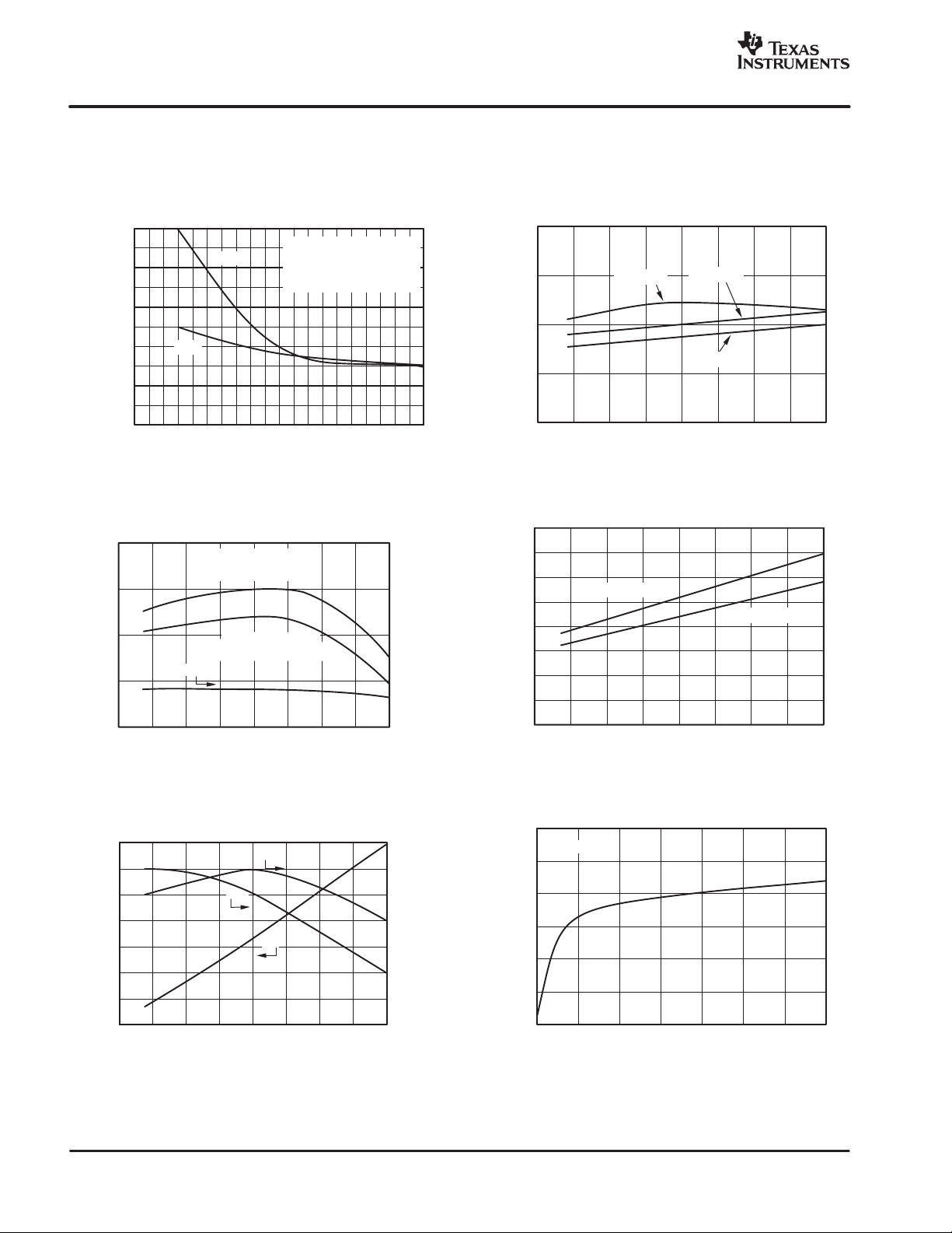
"#$
0
%"#$
&"#$
SBOS099C − SEPTEMBER 2000 − REVISED JANUARY 2005
TYPICAL CHARACTERISTICS (continued)
All specifications at TA = +25°C, VS = +5V , and RL = 1kΩ connected to VS/2, unless otherwise noted.
www.ti.com
DIFFERENTIAL GAIN/PHASE vs RESISTIVE LOAD
0.5
0.4
)
_
0.3
0.2
Differential Gain (%)
Differential Phase (
0.1
0
0 100 200 300 500400 600 800700 900 100
COMMON−MODEAND POWER−SUPPLY REJECTION RATIO
100
90
80
CMRR (dB)
70
60
−75 −50 −25 0 2 5 50 75 100 125
Phase
Gain
Resistive Load (Ω)
vs TEMP ERATUR E
CMRR, VS=5.5V
(VCM=−0.1V to +5.6V)
CMRR, VS=2.7V
(V
CM
PSRR
Temperature (_C)
G=2
=1.4V
V
O
NTSC Signal Generator
SeeFigure6fortestcircuit.
= −0.1Vto +2.8V)
110
100
90
80
70
130
125
120
115
Open−Loop Gain (dB)
110
−
75−50−250255075100125
40
35
30
s)
µ
25
20
PSRR(dB)
15
Slew Rate (V/
10
5
0
−75−50−
OPEN−LOOP GAIN vs TEMPERATURE
Ω
RL=1k
Ω
RL=10k
Ω
RL=600
Temperature (_C)
SLEW RATE vs TEMPERATURE
Negative Slew Rate
Positive Slew Rate
250 255075100125
Temperature (_C)
Quiescent Current (mA)
6
QUIESCENT CURRENT AND
SHORT−CIRCUIT CURRENT vs TEMPERATURE
7.0
6.5
6.0
5.5
5.0
4.5
4.0
3.5
−75−50−
25 0 25 50 75 100 125
Temperature (_C)
+I
I
−
SC
I
Q
QUIESCENT CURRENT vs SUPPLY VOLTAGE
SC
100
90
80
70
60
50
Short−C ircuitCurrent (mA)
40
30
6.0
Per Amplifier
5.5
5.0
4.5
4.0
QuiescentCurrent (mA)
3.5
3.0
2.0 2.5 3.0 3.5 4.0 4.5 5.0 5.5
Supply Voltage (V)
Page 7
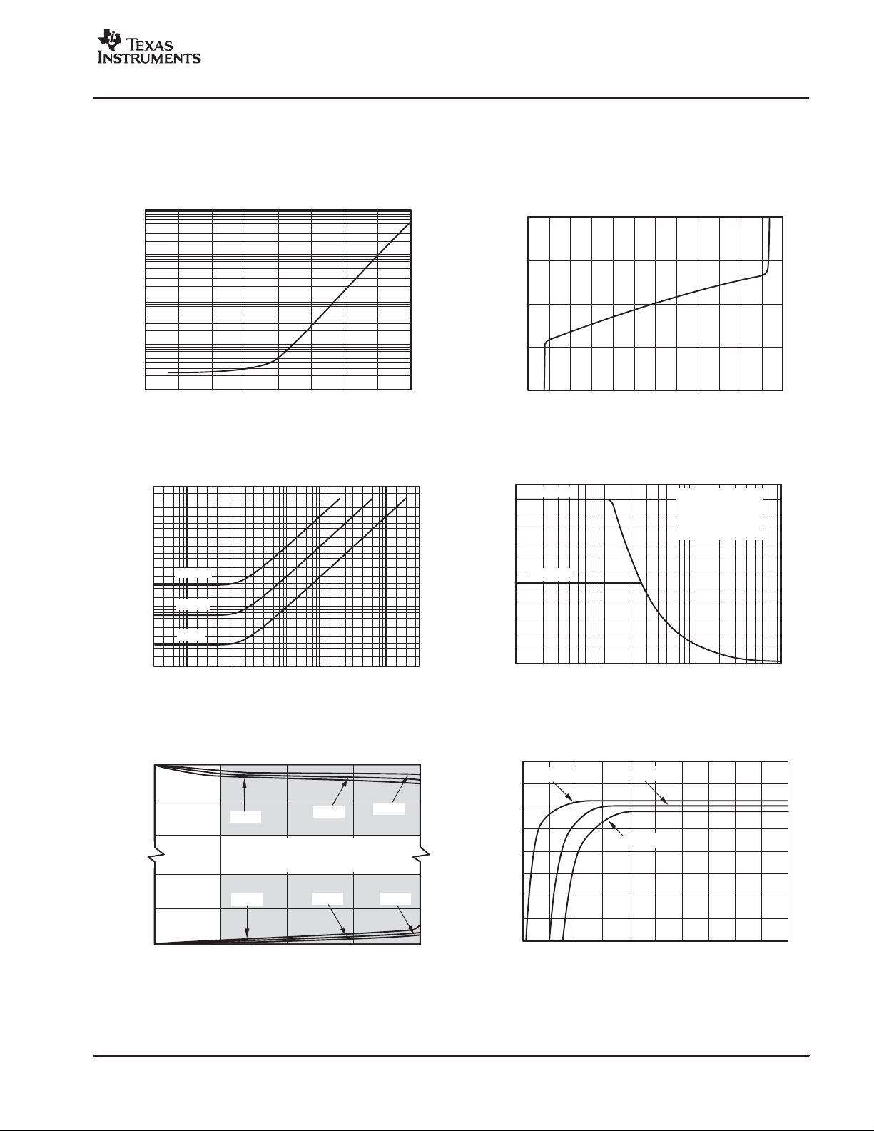
www.ti.com
M
0
SBOS099C − SEPTEMBER 2000 − REVISED JANUARY 2005
TYPICAL CHARACTERISTICS (continued)
All specifications at TA = +25°C, VS = +5V , and RL = 1kΩ connected to VS/2, unless otherwise noted.
"#$
%"#$
&"#$
)
Ω
Output Impedance (
100
Input Bias Current (pA)
0.001
1k
10
1
0.1
100
10
0.1
0.01
INPUT BIAS CURRENT vs TEMPERATURE
−75−50−
CLOSED−LOOP OUTPUT IMPEDANCE vs FREQUENCY
1
25 0 25 50 75 100 125
Temperature (_C)
G = 100
G=10
G=1
INPUT BIAS CURRENT
1.5
1.0
0.5
0.0
Input Bias Current (pA)
−
0.5
−0.5 0.0 0.5 1.0 2.01.5 2.5 3.0 3.5 4.0 5.04.5 5.5
6
5
)
PP
4
3
2
Output Voltage (V
1
vs INPUT COMMON−MODE VOLTAGE
Common−Mode Voltage (V)
MAXIMUM OUTPUT VOLTAGE vs FREQUENCY
VS=5.5V
VS=2.7V
Maximum output
voltage without
slewrate−induced
distortion.
0.0001
1 10 100 1k 10k 100k 1M 10M 100
Frequency (Hz)
OUTPUT VOLTAGE SWING vs OUTPUT CURRENT
V+
(V+)−1
(V+)−2
(V−)+2
Output Voltage (V)
(V−)+1
(V−)
+125_C
Depending on circuit configuration
(including closed−loop gain) performance
may be degraded in shaded region.
+125_C
0
±
10
Output Current (mA)
−55_
+25_C
±
20
0
100k
Frequency (Hz)
OPEN−LOOPGAIN vs OUTPUT VOLTAGE SWING
140
I
=250µA
OUT
130
+25_C
C
−55_
C
±
30
±
4
120
110
100
90
80
Open−Loop Gain (dB)
70
60
0204060 10080 120 160140 180 200
Output Voltage Swing from Rails (mV)
I
I
OUT
=2.5mA
OUT
=4.2mA
100M1M 10M
7
Page 8
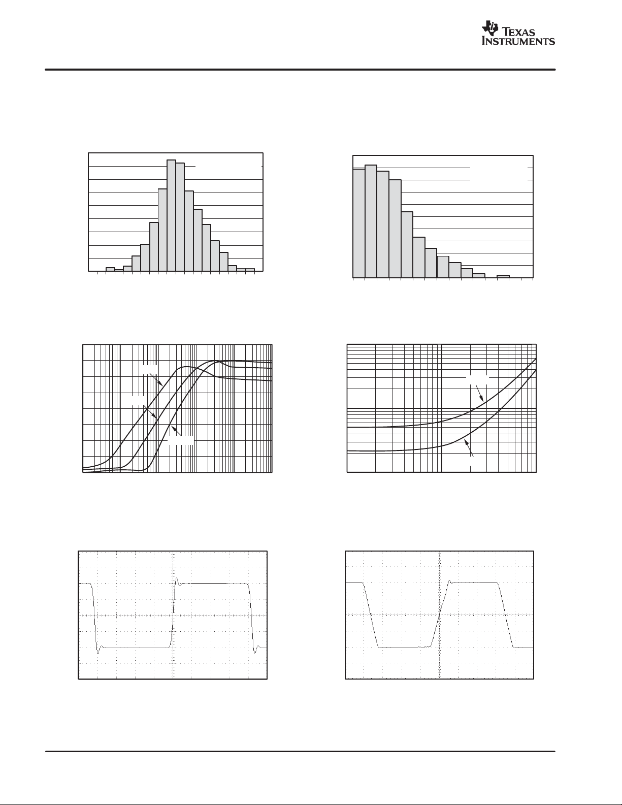
"#$
%"#$
&"#$
SBOS099C − SEPTEMBER 2000 − REVISED JANUARY 2005
TYPICAL CHARACTERISTICS (continued)
All specifications at TA = +25°C, VS = +5V , and RL = 1kΩ connected to VS/2, unless otherwise noted.
www.ti.com
OFFSET VOLTAGE
18
16
14
12
10
8
6
4
Perce n tof Amplifiers (%)
2
0
−500
SMALL−SIGNAL OVERSHOOT vs LOAD CAPACITANCE
80
70
60
50
40
30
Overshoot (%)
20
10
0
10
PRODUC TIONDISTRIBUTION
450−400−350
−
250−200−150−100
−300
−
Offset Voltage (µV)
G=1
G=−1
Load Capacitance (pF)
0
50
−
G=±10
50
Typ ic a ldistributionof
packaged units.
100
150
200
250
300
350
400
450
500
1M100 1k 10k 100k
OFFSET VOLTAGE DRIFT
20
18
16
14
12
10
8
6
Percent of Amplifiers (%)
4
2
0
0123456789101112131415
10
s)
µ
1
Settling Time (
0.1
−
1
PRODUCTION DISTRIBUTION
Typicalproduction
distributi on of
packagedunits.
Offset VoltageDrift (µV/_ C)
SETTLING TIME vs CLOSED−LOOP GAIN
0.01%
0.1%
−
10
Closed−Loop Gain (V/V)
−
100
SMALL−SIGNALSTEP RESPONSE
50mV/div
= 100pF
C
L
100ns/div
1V/div
LARGE−SIGNALSTEP RESPONSE
= 100pF
C
L
200ns/div
8
Page 9
www.ti.com
"#$
%"#$
&"#$
SBOS099C − SEPTEMBER 2000 − REVISED JANUARY 2005
APPLICATIONS INFORMATION
OPA350 series op amps are fabricated on a
state-of-the-art 0.6 micron CMOS process. They are
unity-gain stable and suitable for a wide range of
general-purpose applications. Rail-to-rail input/output
make them ideal for driving sampling A/D converters.
They are also well-suited for controlling the output
power in cell phones. These applications often require
high speed and low noise. In addition, the OPA350
series offers a low-cost solution for general-purpose
and consumer video applications (75Ω drive capability).
Excellent ac performance makes the OPA350 series
well-suited for audio applications. Their bandwidth,
slew rate, low noise (5nV/√Hz), low THD (0.0006%),
and small package options are ideal for these
applications. The class AB output stage is capable of
driving 600Ω loads connected to any point between V+
and ground.
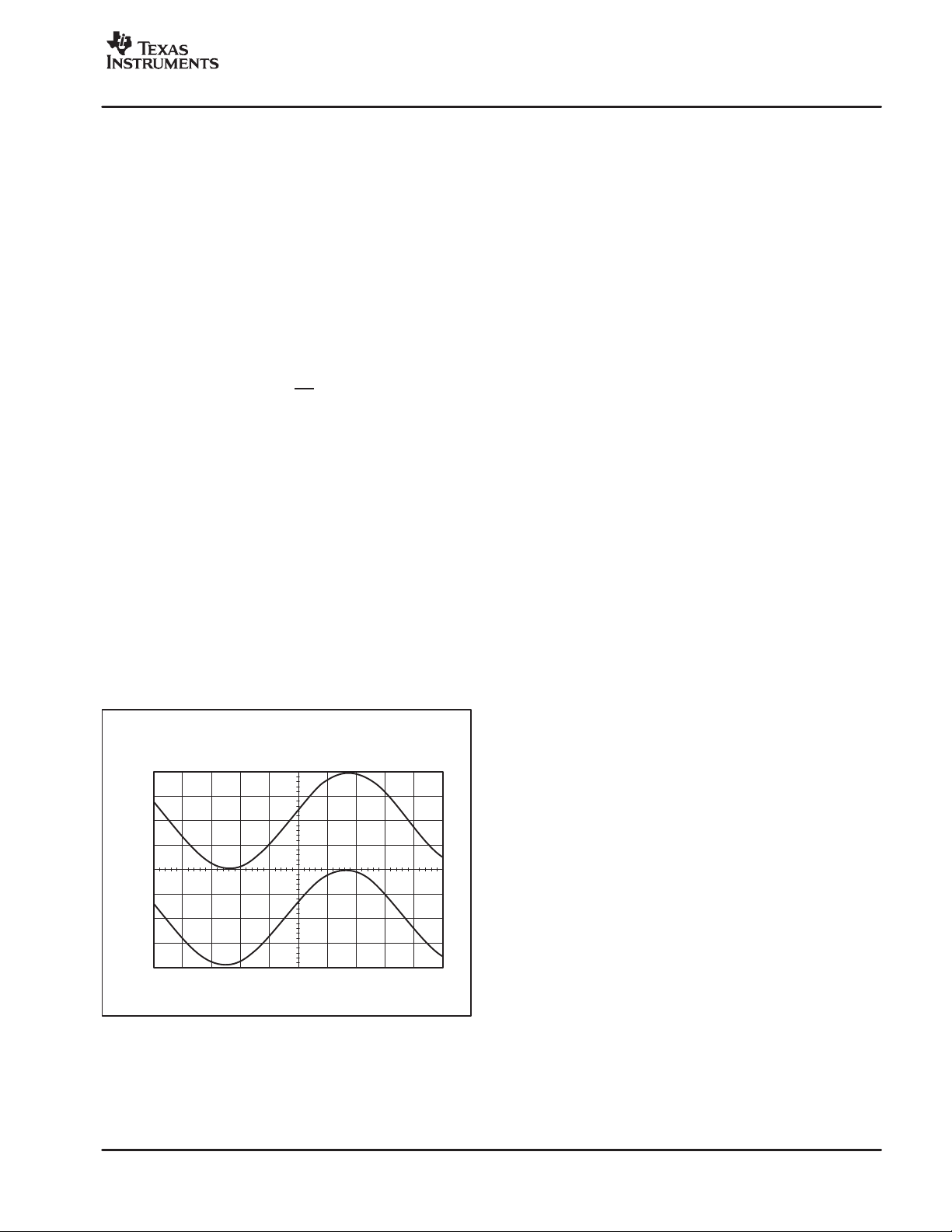
Rail-to-rail input and output swing significantly
increases dynamic range, especially in low voltage
supply applications. Figure 1 shows the input and
output waveforms for the OPA350 in unity-gain
configuration. Operation is from a single +5V supply
with a 1k Ω load connected to VS/2. The input is a 5V
sinusoid. Output voltage swing is approximately
4.95VPP.
Power supply pins should be bypassed with 0.01µF
ceramic capacitors.
5V
V
IN
0
5V
V
OUT
0
VS=+5,G=+1,RL=1k
Ω
Figure 1. Rail-to-Rail Input and Output
PP
1.25V/div
OPERATING VOLTAGE
OPA350 series op amps are fully specified from +2.7V
to +5.5V. However, supply voltage may range from
+2.5V to +5.5V. Parameters are tested over the
specified supply range—a unique feature of the
OPA350 series. In addition, many specifications apply
from −40°C to +85°C. Most behavior remains virtually
unchanged throughout the full operating voltage range.
Parameters that vary significantly with operating
voltage or temperature are shown in the typical
characteristics.
RAIL-TO-RAIL INPUT
The tested input common-mode voltage range of the
OPA350 series extends 100mV beyond the supply rails.
This is achieved with a complementary input stage—an
N-channel input differential pair in parallel with a
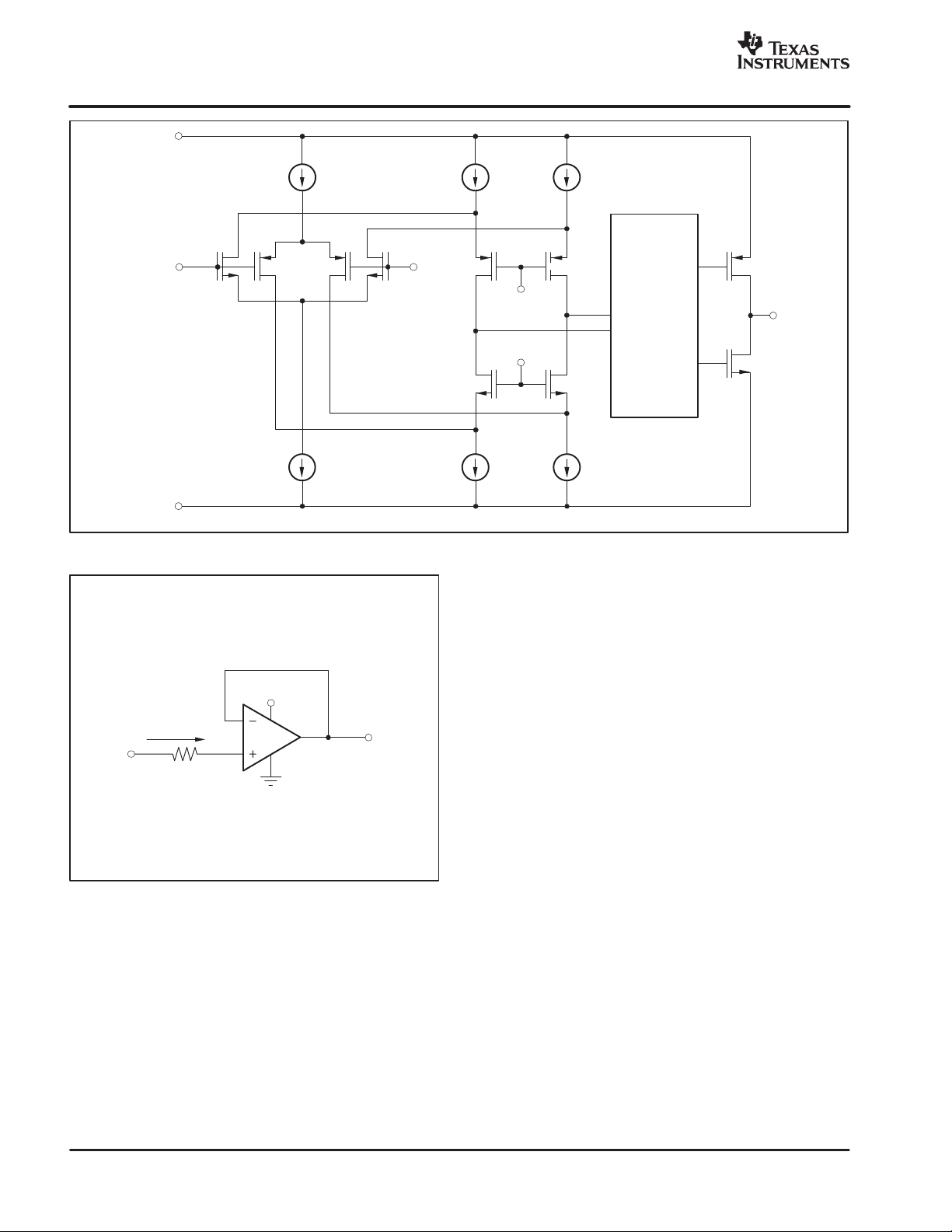
P-channel differential pair, as shown in Figure 2. The
N-channel pair is active for input voltages close to the
positive rail, typically (V+) – 1.8V to 100mV above the
positive supply, while the P-channel pair is on for inputs
from 100mV below the negative supply to
approximately (V+) – 1.8V. There is a small transition
region, typically (V+) – 2V to (V+) – 1.6V, in which both
pairs are on. This 400mV transition region can vary
±400mV with process variation. Thus, the transition
region (both input stages on) can range from (V+) –
2.4V to (V+) – 2.0V on the low end, up to (V+) – 1.6V
to (V+) – 1.2V on the high end.
OPA350 series op amps are laser-trimmed to reduce
offset voltage difference between the N-channel and
P-channel input stages, resulting in improved
common-mode rejection and a smooth transition
between the N-channel pair and the P-channel pair.
However, within the 400mV transition region PSRR,
CMRR, offset voltage, offset drift, and THD may be
degraded compared to operation outside this region.
A double-folded cascode adds the signal from the two
input pairs and presents a differential signal to the class
AB output stage. Normally, input bias current is
approximately 500fA. However, large inputs (greater
than 300mV beyond the supply rails) can turn on the
OPA350’s input protection diodes, causing excessive
current to flow in or out of the input pins. Momentary
voltages greater than 300mV beyond the power supply
can be tolerated if the current on the input pins is limited
to 10mA. This is easily accomplished with an input
resistor, as shown in Figure 3. Many input signals are
inherently current-limited to less than 10mA; therefore,
a limiting resistor is not required.
9
Page 10
"#$
%"#$
&"#$
SBOS099C − SEPTEMBER 2000 − REVISED JANUARY 2005
V+
Reference
Current
www.ti.com
VIN+
V
(Ground)
−
V
IN
Figure 2. Simplified Schematic
V+
I
OVERLOAD
V
IN
10mA max
Ω
5k
OPAx350
V
OUT
Figure 3. Input Current Protection for Voltages
Exceeding the Supply Voltage
RAIL-TO-RAIL OUTPUT
A class AB output stage with common-source
transistors is used to achieve rail-to-rail output. For light
resistive loads (>10kΩ), the output voltage swing is
typically ten mil l i v o l t s f r o m the supply rails. With heavier
resistive loads (600Ω to 10kΩ), the output can swing to
−
V
V
BIAS1
BIAS2
Class AB
Control
Circuitry
within a few tens of millivolts from the supply rails and
maintain high open-loop gain. See the typical
characteristics Output Voltage Swing vs Output Current
and Open-Loop Gain vs Output Voltage.
CAPACITIVE LOAD AND STABILITY
OPA350 series op amps can drive a wide range of
capacitive loads. However, all op amps under certain
conditions may become unstable. Op amp
configuration, gain, and load value are just a few of the
factors to consider when determining stability. An op
amp in unity-gain configuration is the most susceptible
to the effects of capacitive load. The capacitive load
reacts with the op amp’s output impedance, along with
any additional load resistance, to create a pole in the
small-signal response that degrades the phase margin.
In unity gain, OP A350 series op amps perform well with
very large capacitive loads. Increasing gain enhances
the amplifier’s ability to drive more capacitance. The
typical characteristic Small-Signal Overshoot vs
Capacitive Load shows performance with a 1kΩ
resistive load. Increasing load resistance improves
capacitive load drive capability.
V
O
10
Page 11
www.ti.com
"#$
%"#$
&"#$
SBOS099C − SEPTEMBER 2000 − REVISED JANUARY 2005
FEEDBACK CAPACITOR IMPROVES
RESPONSE
For optimum settling time and stability with
high-impedance feedback networks, it may be
necessary to add a feedback capacitor across the
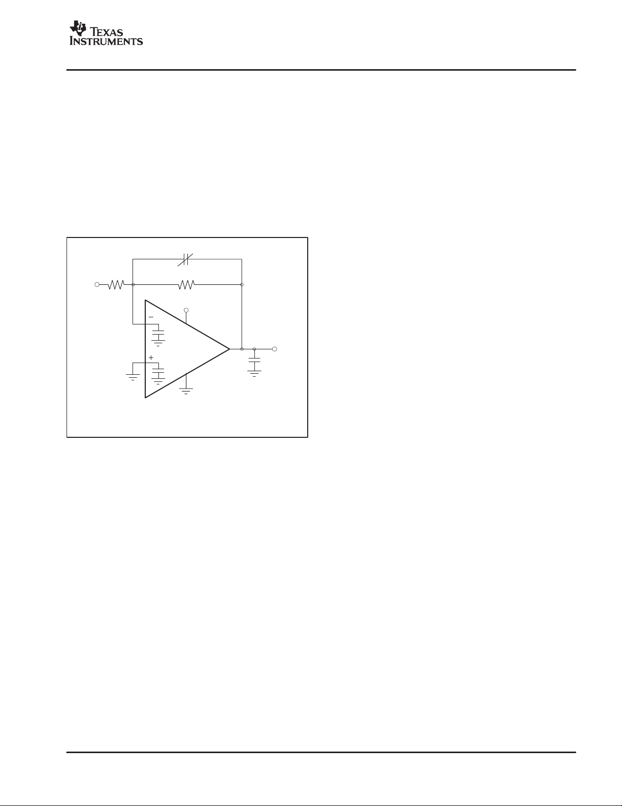
feedback resistor, RF, as shown in Figure 4. This
capacitor compensates for the zero created by the
feedback network impedance and the OPA350’s input
capacitance (and any parasitic layout capacitance).
The effect becomes more significant with higher
impedance networks.
C
F
R
V
R
Where CINis equal to the OPA350’s input
capacitance (approximately 9pF) plus any
parasitic layout capacitance.
IN
IN
•
IN
C
IN=RF
•
C
F
R
F
V+
C
IN
OPA350
C
IN
V
OUT
C
L
Figure 4. Feedback Capacitor Improves Dynamic
Performance
It is suggested that a variable capacitor be used for the
feedback capacitor since input capacitance may vary
between op amps and layout capacitance is difficult to
determine. For the circuit shown in Figure 4, the value
of the variable feedback capacitor should be chosen so
that the input resistance times the input capacitance of
the OP A350 (typically 9pF) plus the estimated parasitic
layout capacitance equals the feedback capacitor times
the feedback resistor:
RIN@ CIN+ RF@ C
F
where CIN is equal to the OPA350’s input capacitance
(sum of differential and common-mode) plus the layout
capacitance. The capacitor can be varied until optimum
performance is obtained.
DRIVING A/D CONVERTERS
OPA350 series op amps are optimized for driving
medium speed (up to 500kHz) sampling A/D
converters. However, they also offer excellent
performance for higher speed converters. The OPA350
series provides an effective means of buffering the
A/D’s input capacitance and resulting charge injection
while providing signal gain.
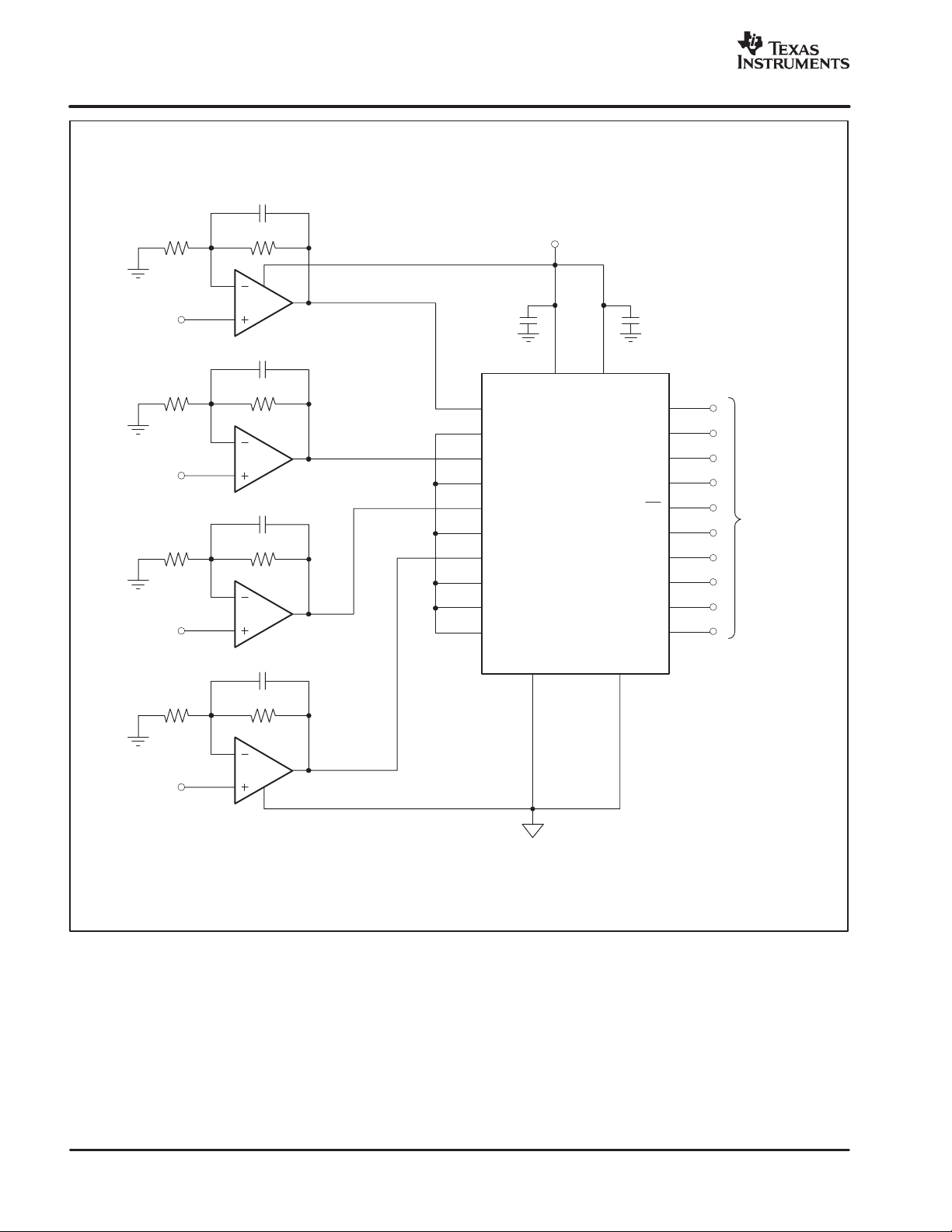
Figure 5 shows the OP A350 driving an ADS7861. The
ADS7861 is a dual, 500kHz, 12-bit sampling converter
in the tiny SSOP-24 package. When used with the
miniature package options of the OPA350 series, the
combination is ideal for space-limited applications. For
further information, consult the ADS7861 data sheet
(SBAS110A).
OUTPUT IMPEDANCE
The low frequency open-loop output impedance of the
OPA350’s common-source output stage is
approximately 1k Ω. When the op amp is connected with
feedback, this value is reduced significantly by the loop
gain of the op amp. For example, with 122dB of
open-loop gain, the output impedance is reduced in
unity-gain to less than 0.001Ω. For each decade rise in
the closed-loop gain, the loop gain is reduced by the
same amount which results in a ten-fold increase in
effective output impedance (see the typical
characteristic, Output Impedance vs Frequency).
At higher frequencies, the output impedance will rise as
the open-loop gain of the op amp drops. However, at
these frequencies the output also becomes capacitive
due to parasitic capacitance. This prevents the output
impedance from becoming too high, which can cause
stability problems when driving capacitive loads. As
mentioned previously, the OPA350 has excellent
capacitive load drive capability for an op amp with its
bandwidth.
VIDEO LINE DRIVER
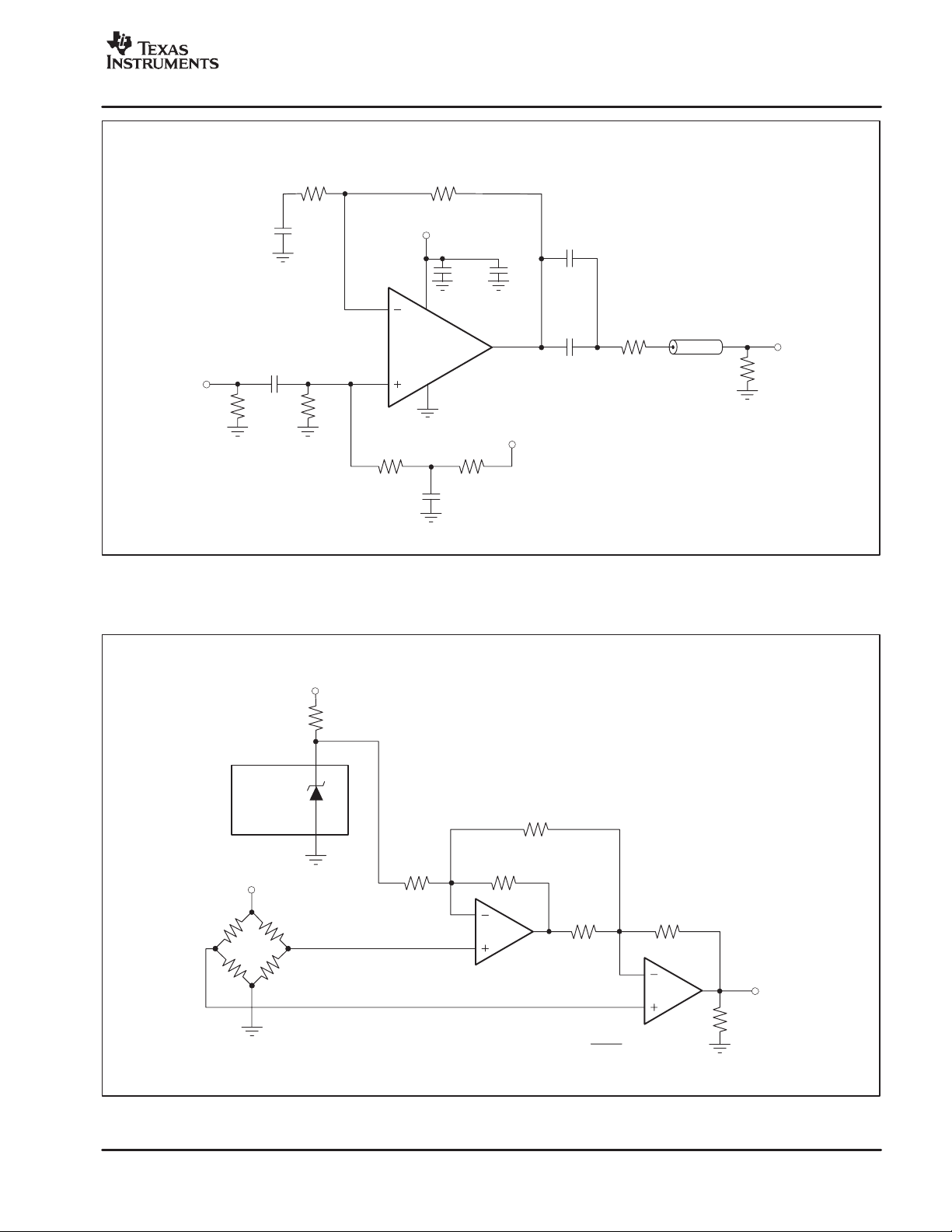
Figure 6 shows a circuit for a single supply, G = 2
composite video line driver. The synchronized outputs
of a composite video line driver extend below ground.
As shown, the input to the op amp should be ac-coupled
and shifted positively to provide adequate signal swing
to account for these negative signals in a single-supply
configuration.
The input is terminated with a 75Ω resistor and
ac-coupled with a 47µF capacitor to a voltage divider
that provides the dc bias point to the input. In Figure 6,
this point is approximately (V−) + 1.7V. Setting the
optimal bias point requires some understanding of the
nature of composite video signals. For best
performance, one should be careful to avoid the
distortion caused by the transition region of the
OPA350’s complementary input stage. Refer to the
discussion of rail-to-rail input.
11
Page 12
"#$
%"#$
&"#$
SBOS099C − SEPTEMBER 2000 − REVISED JANUARY 2005
C
B1
www.ti.com
VINB1
VINB0
VINA1
Ω
6
5
9
10
2
OPA4350
3
OPA4350
OPA4350
1/ 4
1/ 4
1/ 4
2k
4
1
0.1µF0.1
C
B0
Ω
2k
7
C
A1
Ω
2k
8
C
A0
2
CH B1+
3
CH B1
4
CH B0+
5
CH B0
6
CH A1+
7
CH A1
8
CH A0+
9
CH A0
10
REF
11
REF
Ω
2k
Ω
2k
Ω
2k
+5V
24 13
+V
+V
D
A
SERIAL DAT A A
−
SERIAL DATA B
−
ADS7861
−
−
IN
OUT
DGND AGND
BUSY
CLOCK
CS
RD
CONVST
A0
M0
M1
µ
F
23
22
21
20
19
18
Serial
Interface
17
16
15
14
112
Ω
Ω
2k
2k
12
12
1/ 4
OPA4350
VINA0
13
11
VIN= 0V to 2.45V for 0V to 4.9V output.
Choose C
B1,CB0,CA1,CA0
Figure 5. OPA4350 Driving Sampling A/D Converter
14
to filter high frequency noise.
Page 13
www.ti.com
"#$
%"#$
&"#$
SBOS099C − SEPTEMBER 2000 − REVISED JANUARY 2005
Video
In
75
R
C
47µF
1
Ω
2
R
G
Ω
1k
C
1
220µF
2
R
1k
+5V
7
OPA350
F
Ω
+
0.1µF 10µF
6
3
R
2
Ω
5k
R
5k
4
+5V (pin 7)
R
C
10µF
4
Ω
5k
3
3
Ω
Figure 6. Single-Supply Video Line Driver
C
4
0.1µF
C
5
1000µF
R
OUT
Cable
V
OUT
R
L
(2.5V)
REF1004−2.5
+5V
Figure 7. Two Op-Amp Instrumentation Amplifier With
+5V
Ω
50k
8
R
G
4
R
100k
1
Ω
R
2
25k
1/2
OPA2350
Ω
25k
G=5+
R
3
Ω
200k
R
G
R
4
100k
1/2
OPA2350
Ω
Improved High Frequency Common-Mode Rejection
Ω
V
O
R
L
Ω
10k
13
Page 14
"#$
%"#$
&"#$
SBOS099C − SEPTEMBER 2000 − REVISED JANUARY 2005
www.ti.com
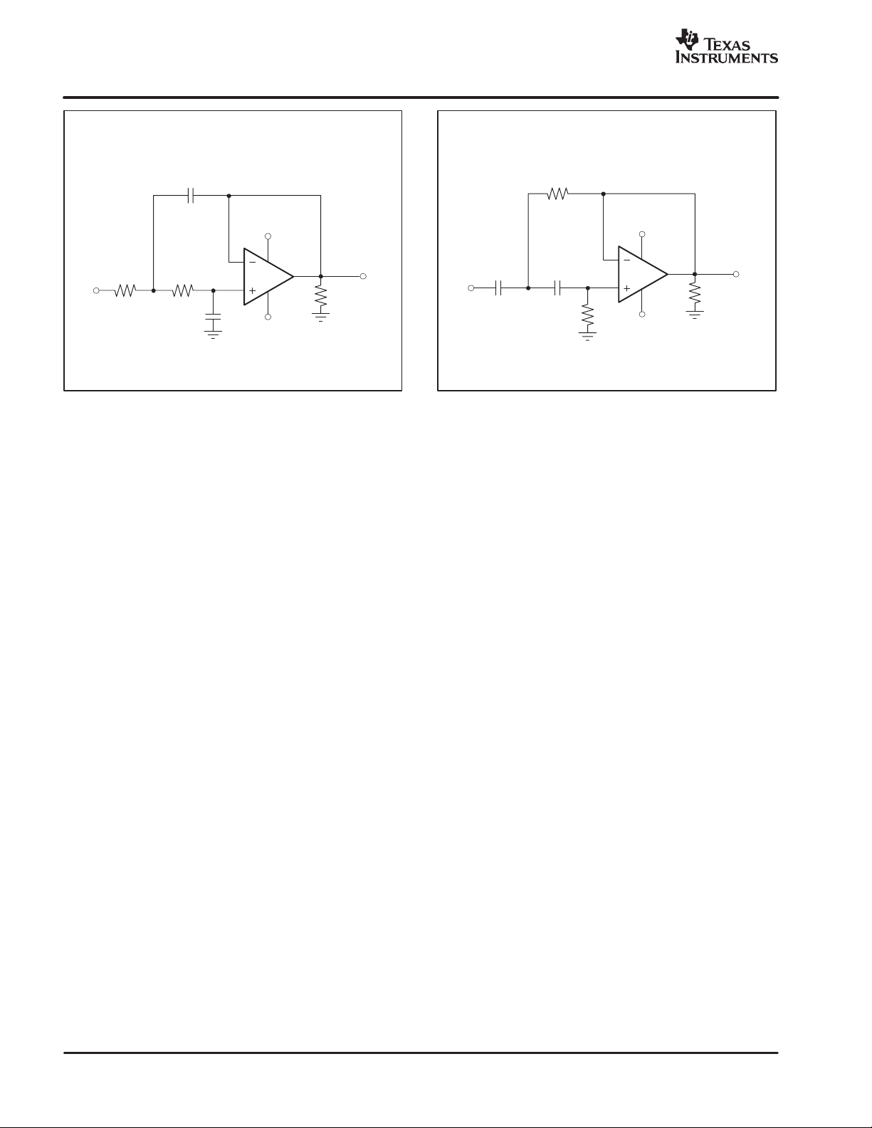
C
1
4.7nF
+2.5V
C
R
1
2.74kΩ
V
IN
R
2
19.6kΩ
C
1nF
OPA350
2
−
2.5V
R
20kΩ
V
OUT
L
V
IN
Figure 8. 10kHz Low-Pass Filter
1
1830pF
Figure 9. 10kHz High-Pass Filter
R
10.5k
C
270pF
49.9k
1
Ω
+2.5V
2
R
2
Ω
OPA350
−2.5V
R
20kΩ
V
OUT
L
14
Page 15

PACKAGE OPTION ADDENDUM
www.ti.com
PACKAGING INFORMATION
Orderable Device Status
OPA2350EA/250 ACTIVE MSOP DGK 8 250 Green (RoHS &
OPA2350EA/250G4 ACTIVE MSOP DGK 8 250 Green (RoHS &
OPA2350EA/2K5 ACTIVE MSOP DGK 8 2500 Green (RoHS &
OPA2350EA/2K5G4 ACTIVE MSOP DGK 8 2500 Green (RoHS &
OPA2350PA ACTIVE PDIP P 8 50 Green (RoHS &
OPA2350PAG4 ACTIVE PDIP P 8 50 Green (RoHS &
OPA2350UA ACTIVE SOIC D 8 100 Green (RoHS &
OPA2350UA/2K5 ACTIVE SOIC D 8 2500 Green (RoHS &
OPA2350UA/2K5G4 ACTIVE SOIC D 8 2500 Green (RoHS &
OPA2350UAG4 ACTIVE SOIC D 8 100 Green (RoHS &
OPA350EA/250 ACTIVE MSOP DGK 8 250 Green (RoHS &
OPA350EA/250G4 ACTIVE MSOP DGK 8 250 Green (RoHS &
OPA350EA/2K5 ACTIVE MSOP DGK 8 2500 Green (RoHS &
OPA350EA/2K5G4 ACTIVE MSOP DGK 8 2500 Green (RoHS &
OPA350PA ACTIVE PDIP P 8 50 Green (RoHS &
OPA350PAG4 ACTIVE PDIP P 8 50 Green (RoHS &
OPA350UA ACTIVE SOIC D 8 100 Green (RoHS &
OPA350UA/2K5 ACTIVE SOIC D 8 2500 Green (RoHS &
OPA350UA/2K5G4 ACTIVE SOIC D 8 2500 Green (RoHS &
OPA350UAG4 ACTIVE SOIC D 8 100 Green (RoHS &
OPA4350EA/250 ACTIVE SSOP/
OPA4350EA/250G4 ACTIVE SSOP/
OPA4350EA/2K5 ACTIVE SSOP/
OPA4350EA/2K5G4 ACTIVE SSOP/
OPA4350UA ACTIVE SOIC D 14 58 Green (RoHS &
(1)
Package
Type
QSOP
QSOP
QSOP
QSOP
Package
Drawing
DBQ 16 250 Green (RoHS &
DBQ 16 250 Green (RoHS &
DBQ 16 2500 Green (RoHS &
DBQ 16 2500 Green (RoHS &
Pins Package
Qty
Eco Plan
no Sb/Br)
no Sb/Br)
no Sb/Br)
no Sb/Br)
no Sb/Br)
no Sb/Br)
no Sb/Br)
no Sb/Br)
no Sb/Br)
no Sb/Br)
no Sb/Br)
no Sb/Br)
no Sb/Br)
no Sb/Br)
no Sb/Br)
no Sb/Br)
no Sb/Br)
no Sb/Br)
no Sb/Br)
no Sb/Br)
no Sb/Br)
no Sb/Br)
no Sb/Br)
no Sb/Br)
no Sb/Br)
(2)
Lead/Ball Finish MSL Peak Temp
CU NIPDAU Level-2-260C-1 YEAR
CU NIPDAU Level-2-260C-1 YEAR
CU NIPDAU Level-2-260C-1 YEAR
CU NIPDAU Level-2-260C-1 YEAR
CU NIPDAU N / A for Pkg Type
CU NIPDAU N / A for Pkg Type
CU NIPDAU Level-2-260C-1 YEAR
CU NIPDAU Level-2-260C-1 YEAR
CU NIPDAU Level-2-260C-1 YEAR
CU NIPDAU Level-2-260C-1 YEAR
CU NIPDAU Level-2-260C-1 YEAR
CU NIPDAU Level-2-260C-1 YEAR
CU NIPDAU Level-2-260C-1 YEAR
CU NIPDAU Level-2-260C-1 YEAR
CU NIPDAU N / A for Pkg Type
CU NIPDAU N / A for Pkg Type
CU NIPDAU Level-2-260C-1 YEAR
CU NIPDAU Level-2-260C-1 YEAR
CU NIPDAU Level-2-260C-1 YEAR
CU NIPDAU Level-2-260C-1 YEAR
CU NIPDAU Level-2-260C-1 YEAR
CU NIPDAU Level-2-260C-1 YEAR
CU NIPDAU Level-2-260C-1 YEAR
CU NIPDAU Level-2-260C-1 YEAR
CU NIPDAU Level-2-260C-1 YEAR
16-Mar-2007
(3)
Addendum-Page 1
Page 16

PACKAGE OPTION ADDENDUM
www.ti.com
Orderable Device Status
(1)
Package
Type
Package
Drawing
Pins Package
Qty
Eco Plan
(2)
OPA4350UA/2K5 ACTIVE SOIC D 14 2500 Green (RoHS &
Lead/Ball Finish MSL Peak Temp
CU NIPDAU Level-2-260C-1 YEAR
16-Mar-2007
(3)
no Sb/Br)
OPA4350UA/2K5G4 ACTIVE SOIC D 14 2500 Green (RoHS &
CU NIPDAU Level-2-260C-1 YEAR
no Sb/Br)
OPA4350UAG4 ACTIVE SOIC D 14 58 Green (RoHS &
CU NIPDAU Level-2-260C-1 YEAR
no Sb/Br)
(1)
The marketing status values are defined as follows:
ACTIVE: Product device recommended for new designs.
LIFEBUY: TI has announced that the device will be discontinued, and a lifetime-buy period is in effect.
NRND: Not recommended for new designs. Device is in production to support existing customers, but TI does not recommend using this part in
a new design.
PREVIEW: Device has been announced but is not in production. Samples may or may not be available.
OBSOLETE: TI has discontinued the production of the device.
(2)
Eco Plan - The planned eco-friendly classification: Pb-Free (RoHS), Pb-Free (RoHS Exempt), or Green (RoHS & no Sb/Br) - please check
http://www.ti.com/productcontent for the latest availability information and additional product content details.
TBD: The Pb-Free/Green conversion plan has not been defined.
Pb-Free (RoHS): TI's terms "Lead-Free" or "Pb-Free" mean semiconductor products that are compatible with the current RoHS requirements
for all 6 substances, including the requirement that lead not exceed 0.1% by weight in homogeneous materials. Where designed to be soldered
at high temperatures, TI Pb-Free products are suitable for use in specified lead-free processes.
Pb-Free (RoHS Exempt): This component has a RoHS exemption for either 1) lead-based flip-chip solder bumps used between the die and
package, or 2) lead-based die adhesive used between the die and leadframe. The component is otherwise considered Pb-Free (RoHS
compatible) as defined above.
Green (RoHS & no Sb/Br): TI defines "Green" to mean Pb-Free (RoHS compatible), and free of Bromine (Br) and Antimony (Sb) based flame
retardants (Br or Sb do not exceed 0.1% by weight in homogeneous material)
(3)
MSL, Peak Temp. -- The Moisture Sensitivity Level rating according to the JEDEC industry standard classifications, and peak solder
temperature.
Important Information and Disclaimer:The information provided on this page represents TI's knowledge and belief as of the date that it is
provided. TI bases its knowledge and belief on information provided by third parties, and makes no representation or warranty as to the
accuracy of such information. Efforts are underway to better integrate information from third parties. TI has taken and continues to take
reasonable steps to provide representative and accurate information but may not have conducted destructive testing or chemical analysis on
incoming materials and chemicals. TI and TI suppliers consider certain information to be proprietary, and thus CAS numbers and other limited
information may not be available for release.
In no event shall TI's liability arising out of such information exceed the total purchase price of the TI part(s) at issue in this document sold by TI
to Customer on an annual basis.
Addendum-Page 2
Page 17
PACKAGE MATERIALS INFORMATION
www.ti.com
3-Aug-2007
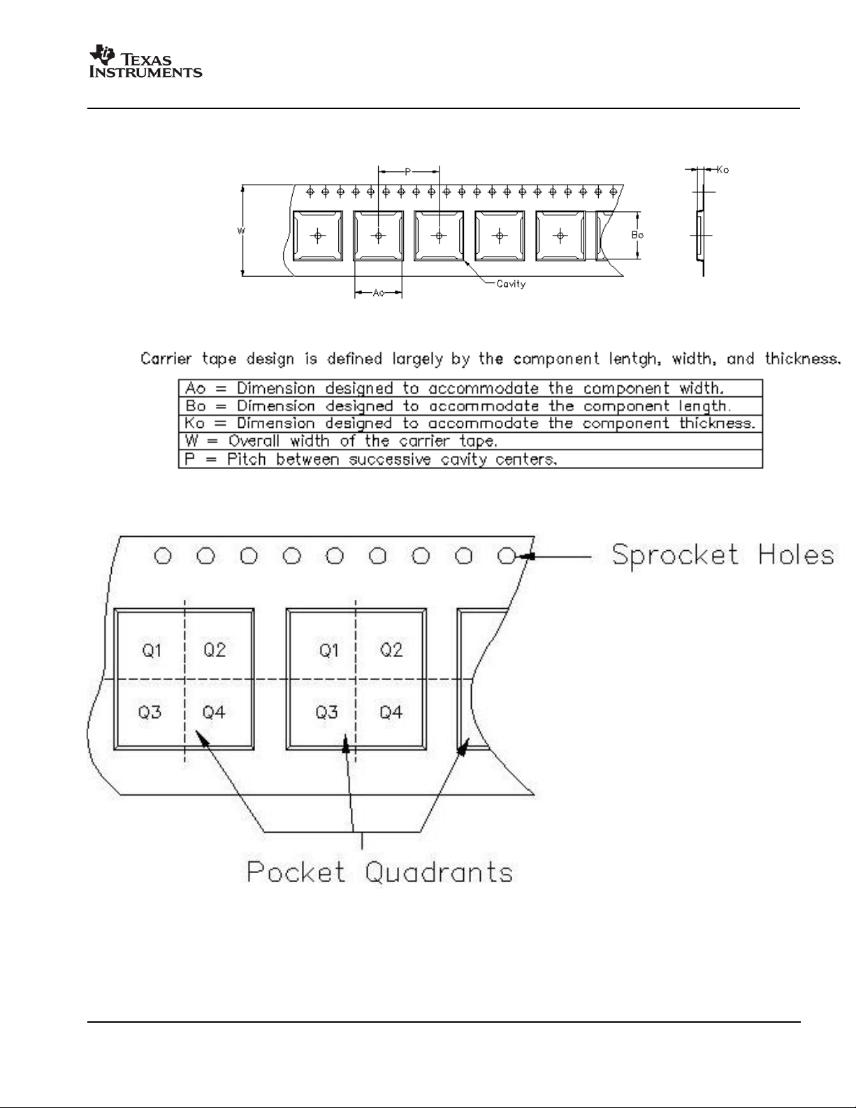
TAPE AND REEL INFORMATION
Pack Materials-Page 1
Page 18
PACKAGE MATERIALS INFORMATION
www.ti.com
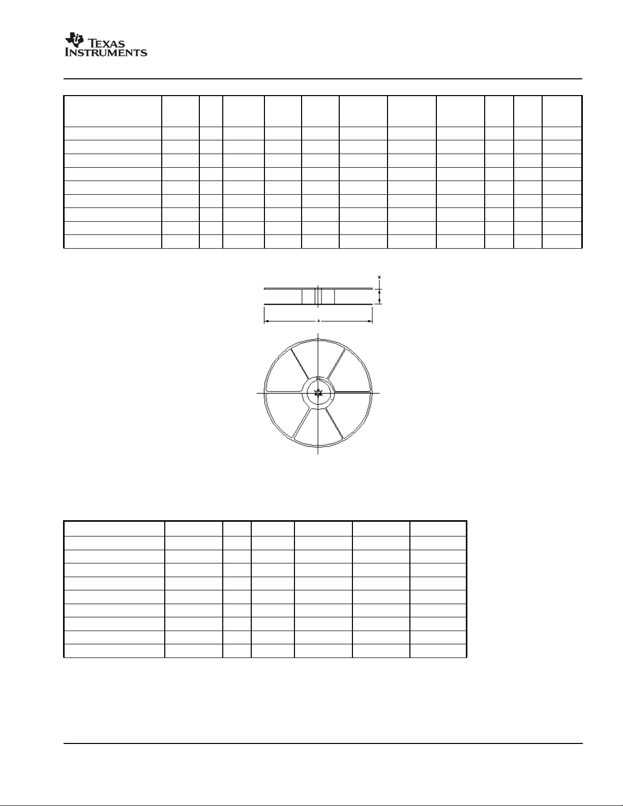
Device Package Pins Site Reel
Diameter
(mm)
OPA2350EA/250 DGK 8 MLA 180 12 5.2 3.3 1.6 12 12 Q1
OPA2350EA/2K5 DGK 8 MLA 330 12 5.2 3.3 1.6 12 12 Q1
OPA2350UA/2K5 D 8 MLA 330 12 6.9 5.4 2.0 8 12 Q1
OPA350EA/250 DGK 8 MLA 180 12 5.2 3.3 1.6 12 12 Q1
OPA350EA/2K5 DGK 8 MLA 330 12 5.2 3.3 1.6 12 12 Q1
OPA350UA/2K5 D 8 MLA 330 12 6.9 5.4 2.0 8 12 Q1
OPA4350EA/250 DBQ 16 TUA 177 12 6.7 5.4 2.1 8 12 Q1
OPA4350EA/2K5 DBQ 16 TUA 330 12 6.7 5.4 2.1 8 12 NONE
OPA4350UA/2K5 D 14 MLA 330 16 6.5 9.5 2.1 8 16 Q1
Reel
Width
(mm)
A0 (mm) B0 (mm) K0 (mm) P1
(mm)W(mm)
3-Aug-2007
Pin1
Quadrant
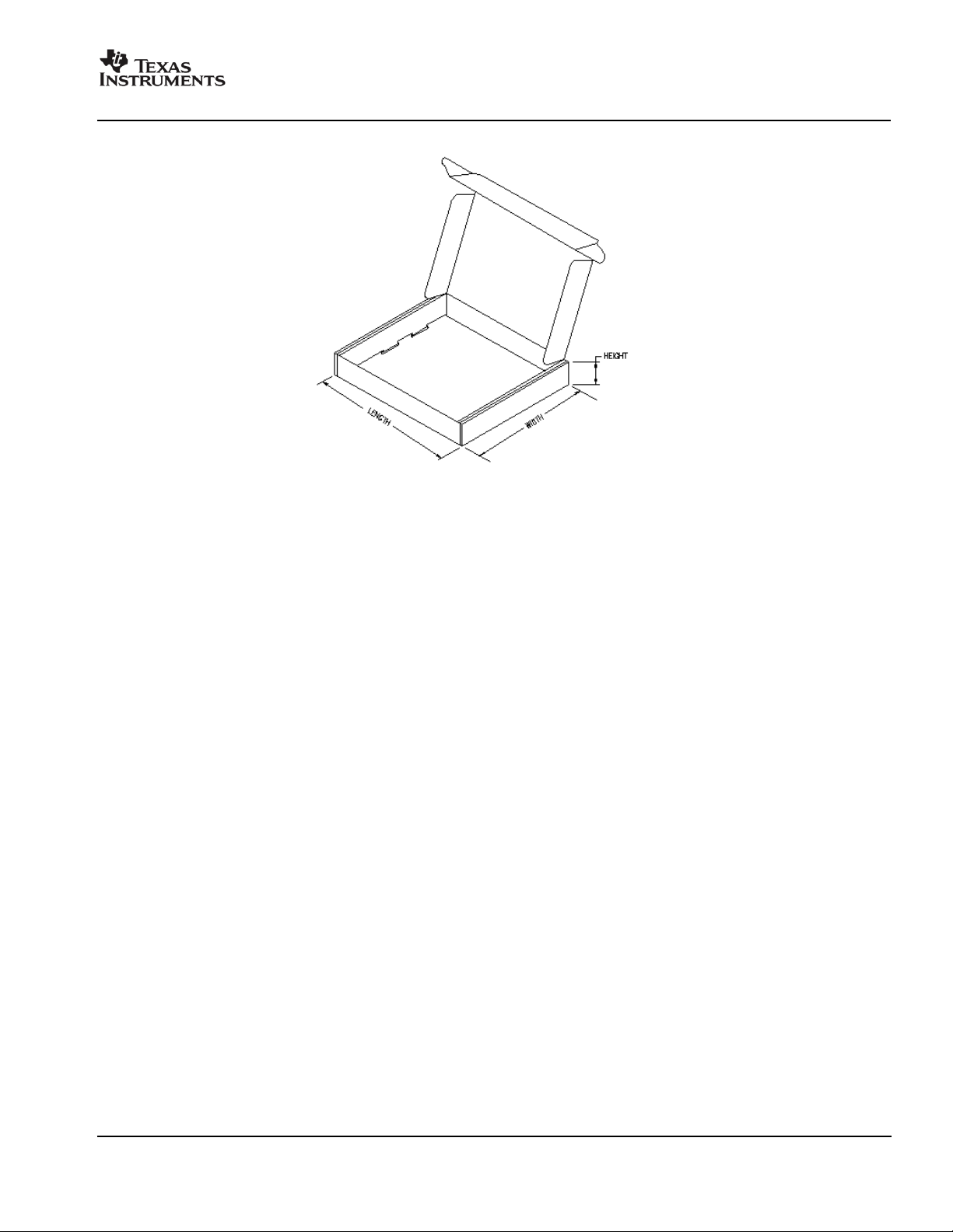
TAPE AND REEL BOX INFORMATION
Device Package Pins Site Length (mm) Width (mm) Height (mm)
OPA2350EA/250 DGK 8 MLA 0.0 0.0 0.0
OPA2350EA/2K5 DGK 8 MLA 346.0 346.0 29.0
OPA2350UA/2K5 D 8 MLA 346.0 346.0 29.0
OPA350EA/250 DGK 8 MLA 0.0 0.0 0.0
OPA350EA/2K5 DGK 8 MLA 346.0 346.0 29.0
OPA350UA/2K5 D 8 MLA 346.0 346.0 29.0
OPA4350EA/250 DBQ 16 TUA 187.0 187.0 25.6
OPA4350EA/2K5 DBQ 16 TUA 375.0 340.0 57.0
OPA4350UA/2K5 D 14 MLA 346.0 346.0 33.0
Pack Materials-Page 2
Page 19
PACKAGE MATERIALS INFORMATION
www.ti.com
3-Aug-2007
Pack Materials-Page 3
Page 20
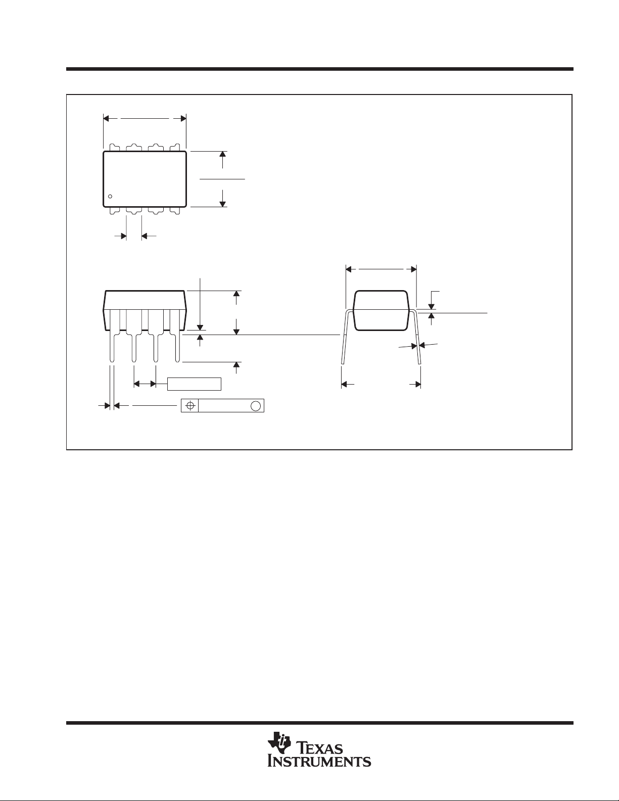
MECHANICAL DATA
MPDI001A – JANUARY 1995 – REVISED JUNE 1999
P (R-PDIP-T8) PLASTIC DUAL-IN-LINE
0.400 (10,60)
0.355 (9,02)
8
5
0.260 (6,60)
0.240 (6,10)
1
0.021 (0,53)
0.015 (0,38)
NOTES: A. All linear dimensions are in inches (millimeters).
B. This drawing is subject to change without notice.
C. Falls within JEDEC MS-001
4
0.070 (1,78) MAX
0.020 (0,51) MIN
0.200 (5,08) MAX
0.125 (3,18) MIN
0.100 (2,54)
0.010 (0,25)
Seating Plane
M
0.325 (8,26)
0.300 (7,62)
0.015 (0,38)
Gage Plane
0.010 (0,25) NOM
0.430 (10,92)
MAX
4040082/D 05/98
For the latest package information, go to http://www.ti.com/sc/docs/package/pkg_info.htm
POST OFFICE BOX 655303 • DALLAS, TEXAS 75265
Page 21
Page 22
Page 23
Page 24
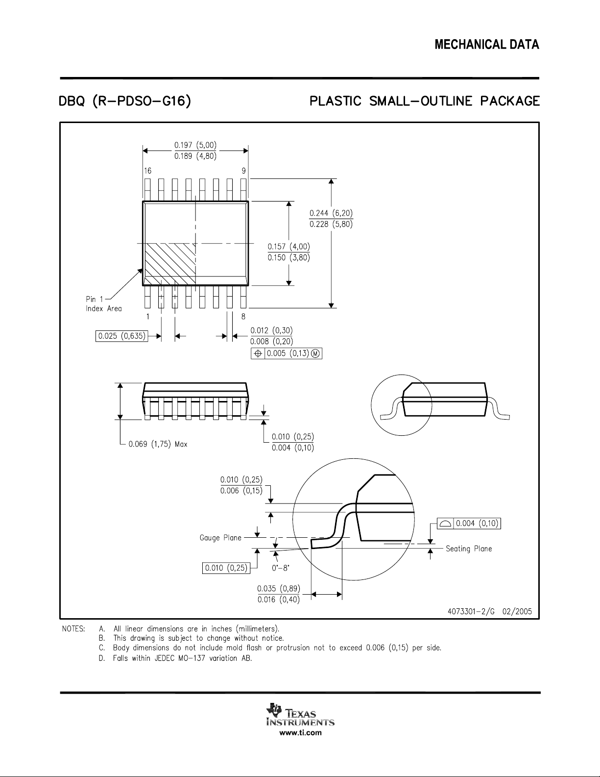
Page 25

IMPORTANT NOTICE
Texas Instruments Incorporated and its subsidiaries (TI) reserve the right to make corrections, modifications, enhancements,
improvements, and other changes to its products and services at any time and to discontinue any product or service without notice.
Customers should obtain the latest relevant information before placing orders and should verify that such information is current and
complete. All products are sold subject to TI’s terms and conditions of sale supplied at the time of order acknowledgment.
TI warrants performance of its hardware products to the specifications applicable at the time of sale in accordance with TI’s
standard warranty. Testing and other quality control techniques are used to the extent TI deems necessary to support this
warranty. Except where mandated by government requirements, testing of all parameters of each product is not necessarily
performed.
TI assumes no liability for applications assistance or customer product design. Customers are responsible for their products and
applications using TI components. To minimize the risks associated with customer products and applications, customers should
provide adequate design and operating safeguards.
TI does not warrant or represent that any license, either express or implied, is granted under any TI patent right, copyright, mask
work right, or other TI intellectual property right relating to any combination, machine, or process in which TI products or services
are used. Information published by TI regarding third-party products or services does not constitute a license from TI to use such
products or services or a warranty or endorsement thereof. Use of such information may require a license from a third party under
the patents or other intellectual property of the third party, or a license from TI under the patents or other intellectual property of TI.
Reproduction of TI information in TI data books or data sheets is permissible only if reproduction is without alteration and is
accompanied by all associated warranties, conditions, limitations, and notices. Reproduction of this information with alteration is an
unfair and deceptive business practice. TI is not responsible or liable for such altered documentation. Information of third parties
may be subject to additional restrictions.
Resale of TI products or services with statements different from or beyond the parameters stated by TI for that product or service
voids all express and any implied warranties for the associated TI product or service and is an unfair and deceptive business
practice. TI is not responsible or liable for any such statements.
TI products are not authorized for use in safety-critical applications (such as life support) where a failure of the TI product would
reasonably be expected to cause severe personal injury or death, unless officers of the parties have executed an agreement
specifically governing such use. Buyers represent that they have all necessary expertise in the safety and regulatory ramifications
of their applications, and acknowledge and agree that they are solely responsible for all legal, regulatory and safety-related
requirements concerning their products and any use of TI products in such safety-critical applications, notwithstanding any
applications-related information or support that may be provided by TI. Further, Buyers must fully indemnify TI and its
representatives against any damages arising out of the use of TI products in such safety-critical applications.
TI products are neither designed nor intended for use in military/aerospace applications or environments unless the TI products are
specifically designated by TI as military-grade or "enhanced plastic." Only products designated by TI as military-grade meet military
specifications. Buyers acknowledge and agree that any such use of TI products which TI has not designated as military-grade is
solely at the Buyer's risk, and that they are solely responsible for compliance with all legal and regulatory requirements in
connection with such use.
TI products are neither designed nor intended for use in automotive applications or environments unless the specific TI products
are designated by TI as compliant with ISO/TS 16949 requirements. Buyers acknowledge and agree that, if they use any
non-designated products in automotive applications, TI will not be responsible for any failure to meet such requirements.
Following are URLs where you can obtain information on other Texas Instruments products and application solutions:
Products Applications
Amplifiers amplifier.ti.com Audio www.ti.com/audio
Data Converters dataconverter.ti.com Automotive www.ti.com/automotive
DSP dsp.ti.com Broadband www.ti.com/broadband
Interface interface.ti.com Digital Control www.ti.com/digitalcontrol
Logic logic.ti.com Military www.ti.com/military
Power Mgmt power.ti.com Optical Networking www.ti.com/opticalnetwork
Microcontrollers microcontroller.ti.com Security www.ti.com/security
RFID www.ti-rfid.com Telephony www.ti.com/telephony
Low Power www.ti.com/lpw Video & Imaging www.ti.com/video
Wireless
Wireless www.ti.com/wireless
Mailing Address: Texas Instruments, Post Office Box 655303, Dallas, Texas 75265
Copyright © 2007, Texas Instruments Incorporated
 Loading...