

Page 1
查询OPA2234P供应商
®
OPA234
OPA234
OPA234
OPA2234
OPA2234
OPA4234
OPA4234
OPA234
OPA2234
OPA4234
For most current data sheet and other product
information, visit www.burr-brown.com
Low Power, Precision
SINGLE-SUPPLY OPERATIONAL AMPLIFIERS
FEATURES
● WIDE SUPPLY RANGE:
Single Supply: VS = +2.7V to +36V
Dual Supply: VS = ±1.35V to ±18V
● GUARANTEED PERFORMANCE:
+2.7V, +5V, and ±15V
● LOW QUIESCENT CURRENT: 250µA/amp
● LOW INPUT BIAS CURRENT: 25nA max
● LOW OFFSET VOLTAGE: 100µV max
● HIGH CMRR, PSRR, and A
OL
● SINGLE, DUAL, and QUAD VERSIONS
DESCRIPTION
The OPA234 series low cost op amps are ideal for
single supply, low voltage, low power applications. The
series provides lower quiescent current than older
“1013”-type products and comes in current industrystandard packages and pinouts. The combination of low
offset voltage, high common-mode rejection, high power
supply rejection, and a wide supply range provides
excellent accuracy and versatility. Single, dual, and
quad versions have identical specifications for maximum design flexibility. These general purpose op amps
are ideal for portable and battery powered applications.
OPA234 series op amps operate from either single or
dual supplies. In single supply operation, the input common-mode range extends below ground and the output
can swing to within 50mV of ground. Excellent phase
margin makes the OPA234 series ideal for demanding
applications, including high load capacitance. Dual and
quad designs feature completely independent circuitry
for lowest crosstalk and freedom from interaction.
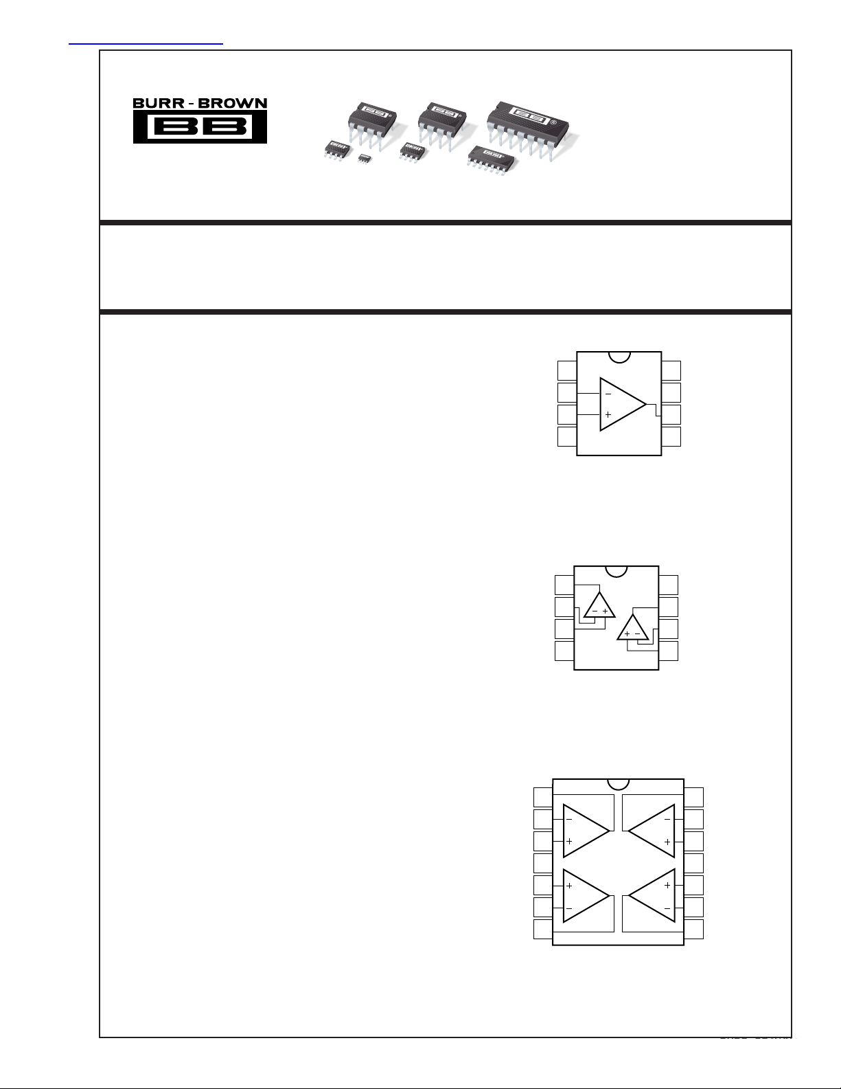
Single version packages are DIP-8, SO-8 surface-mount,
and a space-saving MSOP-8 surface-mount. Dual packages are DIP-8 and SO-8 surface-mount. Quad packages are DIP-14 and SO-14 surface-mount. All are
specified for –40°C to +85°C operation.
Offset Trim
–In
+In
Out A
–In A
+In A
V–
Out A
–In A
+In A
V+
+In B
–In B
Out B
V–
1
2
3
4
5
6
7
OPA234
1
2
3
4
8-Pin DIP, SO-8, MSOP-8
OPA2234
1
A
2
3
4
8-Pin DIP, SO-8
OPA4234
AD
BC
14-Pin DIP
SO-14
8
7
B
6
5
8
7
6
5
NC
V+
Output
Offset Trim
V+
Out B
–In B
+In B
14
13
12
11
10
9
8
Out D
–In D
+In D
V–
+In C
–In C
Out C
International Airport Industrial Park • Mailing Address: PO Box 11400, Tucson, AZ 85734 • Street Address: 6730 S. Tucson Blvd., Tucson, AZ 85706 • Tel: (520) 746-1111
Twx: 910-952-1111 • Internet: http://www.burr-brown.com/ • Cable: BBRCORP • Telex: 066-6491 • FAX: (520) 889-1510 • Immediate Product Info: (800) 548-6132
© 1996 Burr-Brown Corporation PDS-1318B Printed in U.S.A., May, 2000
1
OPA234, 2234, 4234
®
Page 2
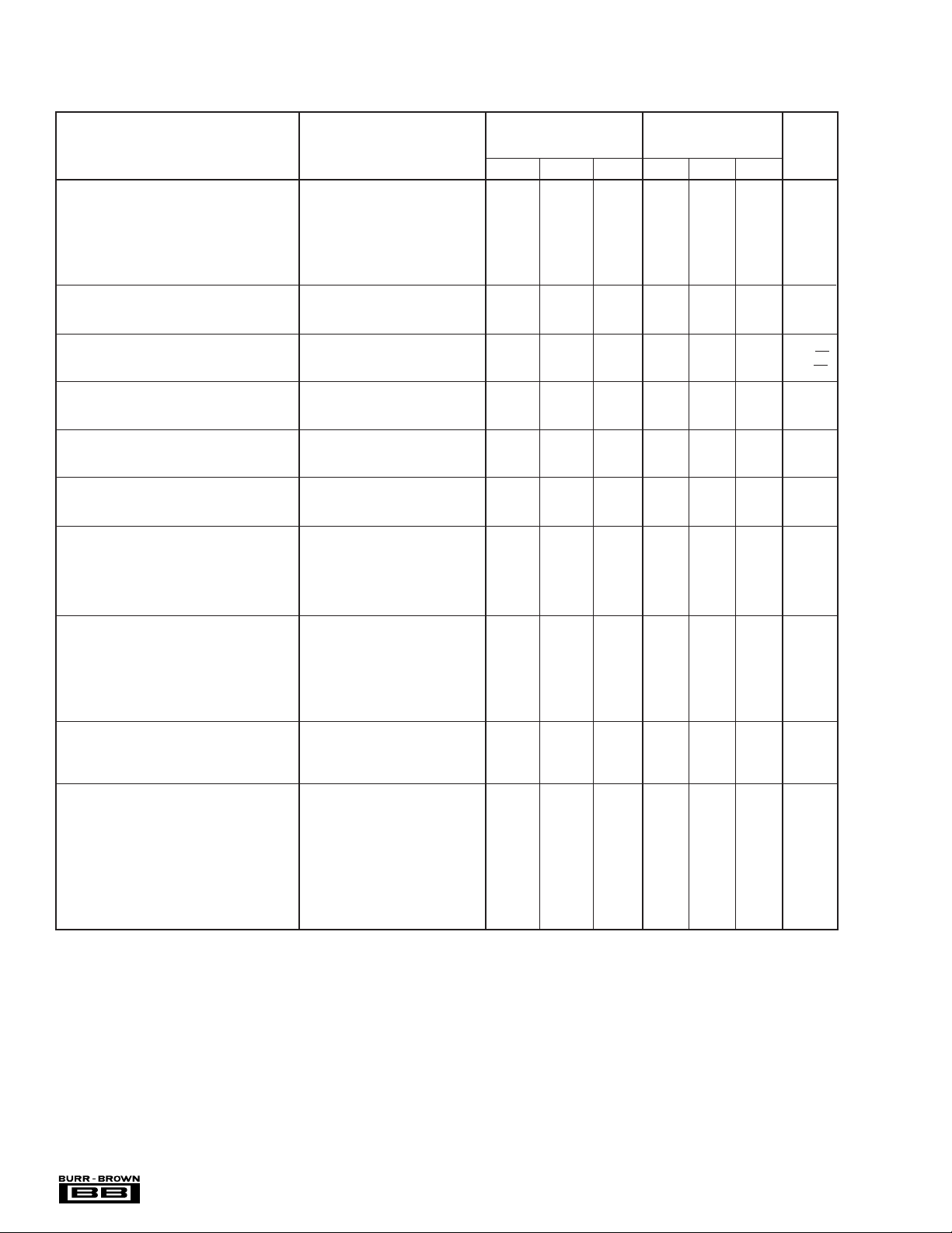
SPECIFICATIONS: VS = +5V
At TA = 25°C, VS = +5V, RL = 10kΩ connected to VS/2 and V
PARAMETER CONDITION MIN TYP MAX MIN TYP MAX UNITS
OFFSET VOLTAGE
Input Offset Voltage V
OPA234E, EA ±100 ±150 ✻ ±350 µV
vs Temperature
(1)
vs Power Supply PSRR V
vs Time 0.2 ✻ µV/mo
OS
dVOS/dT Operating Temperature Range ±0.5 ±3 ✻✻µV/°C
= +2.7V to +30V, V
S
Channel Separation (Dual, Quad) 0.3 ✻ µV/V
INPUT BIAS CURRENT
Input Bias Current
Input Offset Current I
(2)
I
B
OS
NOISE f = 1kHz
Input Voltage Noise Density v
Current Noise Density i
n
n
INPUT VOLTAGE RANGE
Common-Mode Voltage Range –0.1 (V+) –1 ✻✻V
Common-Mode Rejection CMRR V
INPUT IMPEDANCE
Differential 10
Common-Mode V
OPEN-LOOP GAIN V
Open-Loop Voltage Gain A
OL
FREQUENCY RESPONSE
Gain-Bandwidth Product GBW C
Slew Rate SR 0.2 ✻ V/µs
Settling Time: 0.1% G = 1, 3V Step, C
0.01% G = 1, 3V Step, C
Overload Recovery Time (V
OUTPUT
Voltage Output: Positive R
Negative R
Positive R
Negative R
Short-Circuit Current I
Capacitive Load Drive (Stable Operation)
SC
(3)
POWER SUPPLY
Specified Operating Voltage +5 ✻ V
Operating Voltage Range +2.7 +36 ✻✻V
Quiescent Current (per amplifier) I
Q
TEMPERATURE RANGE
Specified Range –40 +85 ✻✻°C
Operating Range –40 +125 ✻✻°C
Storage –55 +125 ✻✻°C
Thermal Resistance
8-Pin DIP 100 ✻ °C/W
θ
JA
SO-8 Surface-Mount 150 ✻ °C/W
MSOP-8 Surface-Mount 220 ✻ °C/W
14-Pin DIP 80 ✻ °C/W
SO-14 Surface-Mount 110 ✻ °C/W
✻ Specifications same as OPA234P,U,E.
NOTES: (1) Guaranteed by wafer-level test to 95% confidence level. (2) Positive conventional current flows into the input terminals. (3) See “Small-Signal Overshoot
vs Load Capacitance” typical curve.
= VS/2, unless otherwise noted.
OUT
OPA234PA, UA, EA
OPA234P, U, E
OPA2234P, U
V
= 2.5V ±40 ±100 ✻ ±250 µV
CM
= 1.7V 3 10 ✻ 20 µV/V
CM
V
= 2.5V –15 –30 ✻ –50 nA
CM
V
= 2.5V ±1 ±5 ✻✻nA
CM
OPA2234PA, UA
OPA4234PA, UA, U
25 ✻ nV/√Hz
80 ✻ fA/√Hz
= –0.1V to 4V 91 106 86 ✻ dB
CM
7
|| 5 ✻ Ω || pF
= 2.5V 10
CM
= 0.25V to 4V
O
RL = 10kΩ 108 120 100 ✻ dB
R
= 2kΩ 86 96 86 ✻ dB
L
= 100pF 0.35 ✻ MHz
L
= 100pF 15 ✻ µs
L
= 100pF 25 ✻ µs
L
) (Gain) = V
IN
= 10kΩ to VS/2 (V+) –1
L
= 10kΩ to VS/2 0.25 0.05 ✻✻ V
L
= 10kΩ to Ground (V+) –1
L
= 10kΩ to Ground 0.1 0.05 ✻✻ V
L
S
10
|| 6 ✻ Ω || pF
16 ✻ µs
(V+) –0.65
(V+) –0.65
✻✻ V
✻✻ V
±11 ✻ mA
G = +1 1000 ✻ pF
IO = 0 250 300 ✻✻µA
The information provided herein is believed to be reliable; however, BURR-BROWN assumes no responsibility for inaccuracies or omissions. BURR-BROWN assumes
no responsibility for the use of this information, and all use of such information shall be entirely at the user’s own risk. Prices and specifications are subject to change
without notice. No patent rights or licenses to any of the circuits described herein are implied or granted to any third party. BURR-BROWN does not authorize or warrant
any BURR-BROWN product for use in life support devices and/or systems.
®
OPA234, 2234, 4234
2
Page 3
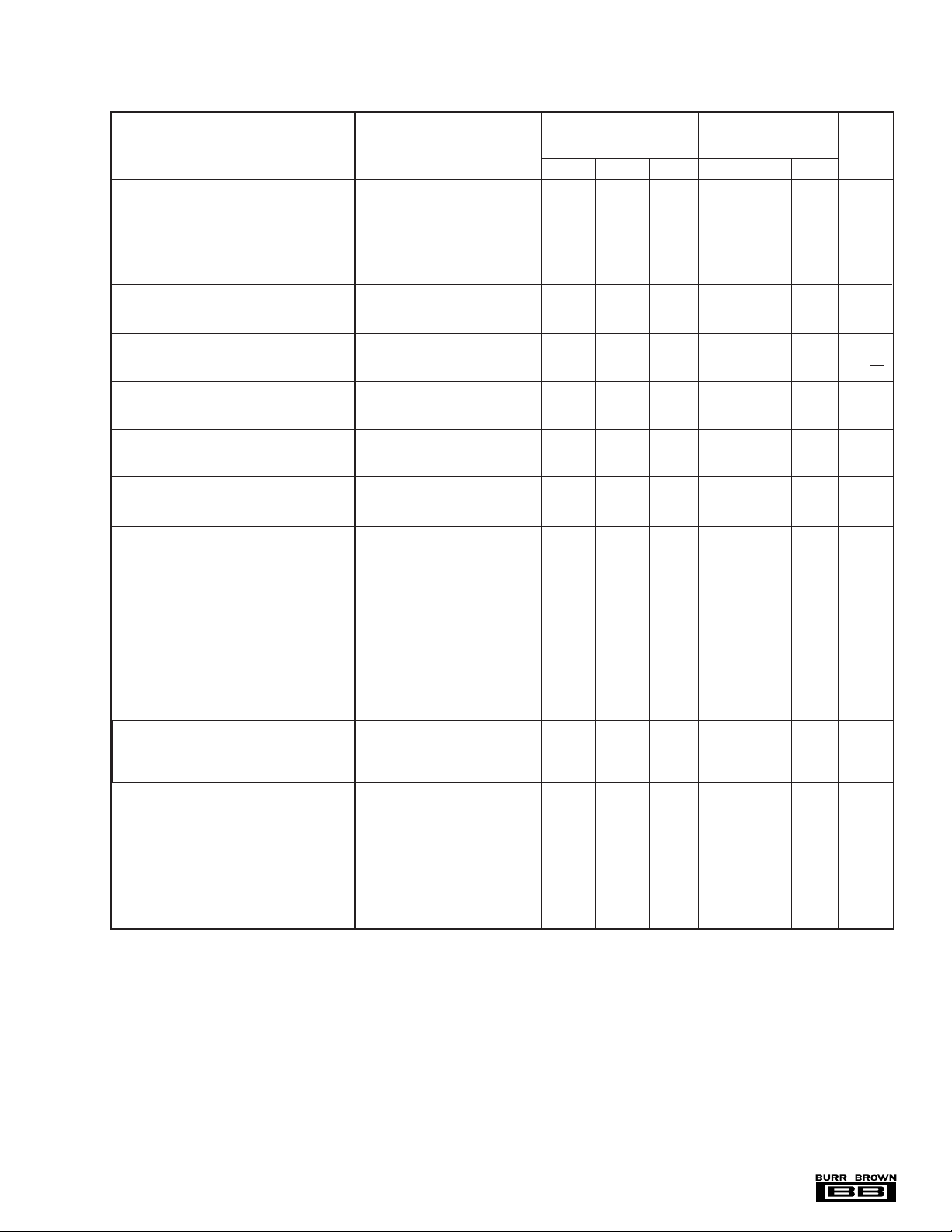
SPECIFICATIONS: VS = +2.7V
At TA = 25°C, VS = +2.7V, RL = 10kΩ connected to VS/2 and V
PARAMETER CONDITION MIN TYP MAX MIN TYP MAX UNITS
OFFSET VOLTAGE
Input Offset Voltage V
OPA234E, EA ±100 ±150 ✻ ±350 µV
vs Temperature
(1)
vs Power Supply PSRR V
vs Time 0.2 ✻ µV/mo
OS
dVOS/dT Operating Temperature Range ±0.5 ±3 ✻✻µV/°C
= +2.7V to +30V, V
S
Channel Separation (Dual, Quad) 0.3 ✻ µV/V
INPUT BIAS CURRENT
Input Bias Current
Input Offset Current I
(2)
I
B
OS
NOISE f = 1kHz
Input Voltage Noise Density v
Current Noise Density i
n
n
INPUT VOLTAGE RANGE
Common-Mode Voltage Range –0.1 (V+) –1 ✻✻V
Common-Mode Rejection CMRR V
INPUT IMPEDANCE
Differential 10
Common-Mode V
OPEN-LOOP GAIN V
Open-Loop Voltage Gain A
OL
FREQUENCY RESPONSE
Gain-Bandwidth Product GBW C
Slew Rate SR 0.2 ✻ V/µs
Settling Time: 0.1% G = 1, 1V Step, C
0.01% G = 1, 1V Step, C
Overload Recovery Time (V
OUTPUT
Voltage Output: Positive R
Negative R
Positive R
Negative R
Short-Circuit Current I
Capacitive Load Drive (Stable Operation)
SC
(3)
POWER SUPPLY
Specified Operating Voltage +2.7 ✻ V
Operating Voltage Range +2.7 +36 ✻✻V
Quiescent Current (per amplifier) I
Q
TEMPERATURE RANGE
Specified Range –40 +85 ✻✻°C
Operating Range –40 +125 ✻✻°C
Storage –55 +125 ✻✻°C
Thermal Resistance
8-Pin DIP 100 ✻ °C/W
θ
JA
SO-8 Surface-Mount 150 ✻ °C/W
MSOP-8 Surface-Mount 220 ✻ °C/W
14-Pin DIP 80 ✻ °C/W
SO-14 Surface-Mount 110 ✻ °C/W
✻ Specifications same as OPA234P,U,E.
NOTES: (1) Guaranteed by wafer-level test to 95% confidence level. (2) Positive conventional current flows into the input terminals. (3) See “Small-Signal Overshoot
vs Load Capacitance” typical curve.
= VS/2, unless otherwise noted.
OUT
OPA234PA, UA, EA
OPA234P, U, E
OPA2234P, U
V
= 1.35V ±40 ±100 ✻ ±250 µV
CM
= 1.7V 3 10 ✻ 20 µV/V
CM
V
= 1.35V –15 –30 ✻ –50 nA
CM
V
= 1.35V ±1 ±5 ✻✻ n
CM
OPA2234PA, UA
OPA4234PA, UA, U
25 ✻ nV/√Hz
80 ✻ fA/√Hz
= –0.1V to 1.7V 91 106 86 ✻ dB
CM
7
|| 5 ✻ Ω || pF
= 1.35V 10
CM
= 0.25V to 1.7V
O
RL = 10kΩ 108 125 100 ✻ dB
R
= 2kΩ 86 96 86 ✻ dB
L
= 100pF 0.35 ✻ MHz
L
= 100pF 6 ✻ µs
L
= 100pF 16 ✻ µs
L
(Gain) = V
IN)
= 10kΩ to VS/2 (V+) –1 (V+) –0.6 ✻✻ V
L
= 10kΩ to VS/2 0.25 0.05 ✻✻ V
L
= 10kΩ to Ground (V+) –1
L
= 10kΩ to Ground 0.1 0.05 ✻✻ V
L
S
10
|| 6 ✻ Ω || pF
8 ✻ µs
(V+) –0.65
✻✻ V
±8 ✻ mA
G = +1 1000 ✻ pF
IO = 0 250 300 ✻✻µA
®
3
OPA234, 2234, 4234
Page 4
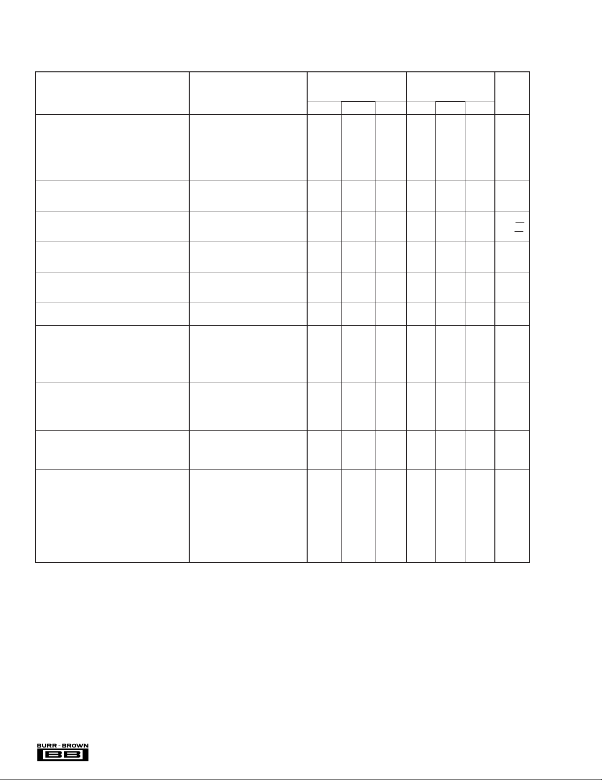
SPECIFICATIONS: VS = ±15V
At TA = 25°C, VS = ±15V, RL = 10kΩ connected to ground, unless otherwise noted.
OPA234P, U, E
OPA2234P, U
OPA2234PA, UA
OPA4234PA, UA, U
PARAMETER CONDITION MIN TYP MAX MIN TYP MAX UNITS
OFFSET VOLTAGE
OPA234PA, UA, EA
Input Offset Voltage V
OPA4234U Model ±70 ±250 µV
vs Temperature
(1)
vs Power Supply PSRR V
vs Time 0.2 ✻ µV/mo
OS
dVOS/dT Operating Temperature Range ±0.5 ±5 ✻✻µV/°C
S
V
= 0V ±70 ±250 ✻ ±500 µV
CM
= ±1.35V to ±18V, V
= 0V 3 10 ✻ 20 µV/V
CM
Channel Separation (Dual, Quad) 0.3 ✻ µV/V
INPUT BIAS CURRENT
Input Bias Current
Input Offset Current I
(2)
I
B
OS
V
= 0V –12 –25 ✻ –50 nA
CM
V
= 0V ±1 ±5 ✻✻nA
CM
NOISE f = 1kHz
Input Voltage Noise Density v
Current Noise Density i
n
n
25 ✻ nV/√Hz
80 ✻ fA/√Hz
INPUT VOLTAGE RANGE
Common-Mode Voltage Range (V–) (V+) –1 ✻✻V
Common-Mode Rejection CMRR V
INPUT IMPEDANCE
Differential 10
Common-Mode V
= –15V to 14V 91 106 86 ✻ dB
CM
7
|| 5 ✻ Ω || pF
= 0V 10
CM
10
|| 6 ✻ Ω || pF
OPEN-LOOP GAIN
Open-Loop Voltage Gain A
OL
VO = –14.5V to 14V 110 120 100 ✻ dB
FREQUENCY RESPONSE
Gain-Bandwidth Product GBW C
Slew Rate SR 0.2 ✻ V/µs
Settling Time: 0.1% G = 1, 10V Step, C
0.01% G = 1, 10V Step, C
Overload Recovery Time (V
= 100pF 0.35 ✻ MHz
L
= 100pF 41 ✻ µs
L
= 100pF 47 ✻ µs
L
) (Gain) = V
IN
S
22 ✻ µs
OUTPUT
Voltage Output: Positive (V+) –1 (V+) –0.7 ✻✻ V
Short-Circuit Current I
Negative (V–) +0.5
Capacitive Load Drive (Stable Operation)
SC
(3)
G = +1 1000 ✻ pF
(V–) +0.15
✻✻ V
±22 ✻ mA
POWER SUPPLY
Specified Operating Voltage ±15 ✻ V
Operating Voltage Range ±1.35 ±18 ✻✻V
Quiescent Current (per amplifier) I
Q
IO = 0 ±275 ±350 ✻✻µA
TEMPERATURE RANGE
Specified Range –40 +85 ✻✻°C
Operating Range –40 +125 ✻✻°C
Storage –55 +125 ✻✻°C
Thermal Resistance
8-Pin DIP 100 ✻ °C/W
θ
JA
SO-8 Surface-Mount 150 ✻ °C/W
MSOP-8 Surface-Mount 220 ✻ °C/W
14-Pin DIP 80 ✻ °C/W
SO-14 Surface-Mount 110 ✻ °C/W
✻ Specifications same as OPA234P,U,E.
NOTES: (1) Guaranteed by wafer-level test to 95% confidence level. (2) Positive conventional current flows into the input terminals. (3) See “Small-Signal Overshoot
vs Load Capacitance” typical curve.
®
OPA234, 2234, 4234
4
Page 5
ELECTROSTATIC
DISCHARGE SENSITIVITY
This integrated circuit can be damaged by ESD. Burr-Brown
recommends that all integrated circuits be handled with
appropriate precautions. Failure to observe proper handling
and installation procedures can cause damage.
ABSOLUTE MAXIMUM RATINGS
Supply Voltage, V+ to V– .................................................................... 36V
Input Voltage ..................................................... (V–) –0.7V to (V+) +0.7V
Output Short-Circuit
Operating Temperature .................................................. –40°C to +125°C
Storage Temperature .....................................................–55 °C to +125°C
Junction Temperature ...................................................................... 150°C
Lead Temperature (soldering, 10s) ................................................. 300°C
NOTE: (1) Short-circuit to ground, one amplifier per package.
(1)
.............................................................. Continuous
ESD damage can range from subtle performance degradation to complete device failure. Precision integrated circuits
may be more susceptible to damage because very small
parametric changes could cause the device not to meet its
published specifications.
PACKAGE/ORDERING INFORMATION
PACKAGE SPECIFIED
PRODUCT PACKAGE NUMBER RANGE MARKING NUMBER
Single
OPA234EA MSOP-8 Surface-Mount 337 –40°C to +85°C A34
"""""OPA234EA/2K5 Tape and Reel
OPA234E MSOP-8 Surface-Mount 337 –40°C to +85°C A34
DRAWING TEMPERATURE PACKAGE ORDERING TRANSPORT
(2)
(2)
OPA234EA/250 Tape and Reel
OPA234E/250 Tape and Reel
"""""OPA234E/2K5 Tape and Reel
OPA234PA Plastic DIP-8 006 –40°C to +85°C OPA234PA OPA234PA Rails
OPA234P
OPA234UA SO-8 Surface-Mount 182 –40°C to +85°C OPA234UA OPA234UA Rails
OPA234U
Dual
OPA2234PA Plastic DIP-8 006 –40°C to +85°C OPA2234PA OPA2234PA Rails
OPA2234P
OPA2234UA SO-8 Surface-Mount 182 –40°C to +85°C OPA2234UA OPA2234UA Rails
OPA2234U
Quad
OPA4234PA Plastic DIP-8 006 –40°C to +85°C OPA4234PA OPA4234PA Rails
OPA4234P
OPA4234UA SO-8 Surface-Mount 182 –40°C to +85°C OPA4234UA OPA4234UA Rails
OPA4234U
NOTE: (1) Models with a slash (/) are available only in Tape and Reel in the quantities indicated (e.g., /2K5 indicates 2500 devices per reel). Ordering 2500 pieces
of “OPA234E//2K5” will get a single 2500-piece Tape and Reel. (2) The grade will be marked on the Reel.
"""OPA234P OPA234P Rails
"""OPA234U OPA234U Rails
"""OPA2234P OPA2234P Rails
"""OPA2234U OPA2234U Rails
"""OPA4234P OPA4234P Rails
"""OPA4234U OPA4234U Rails
(1)
MEDIA
®
5
OPA234, 2234, 4234
Page 6
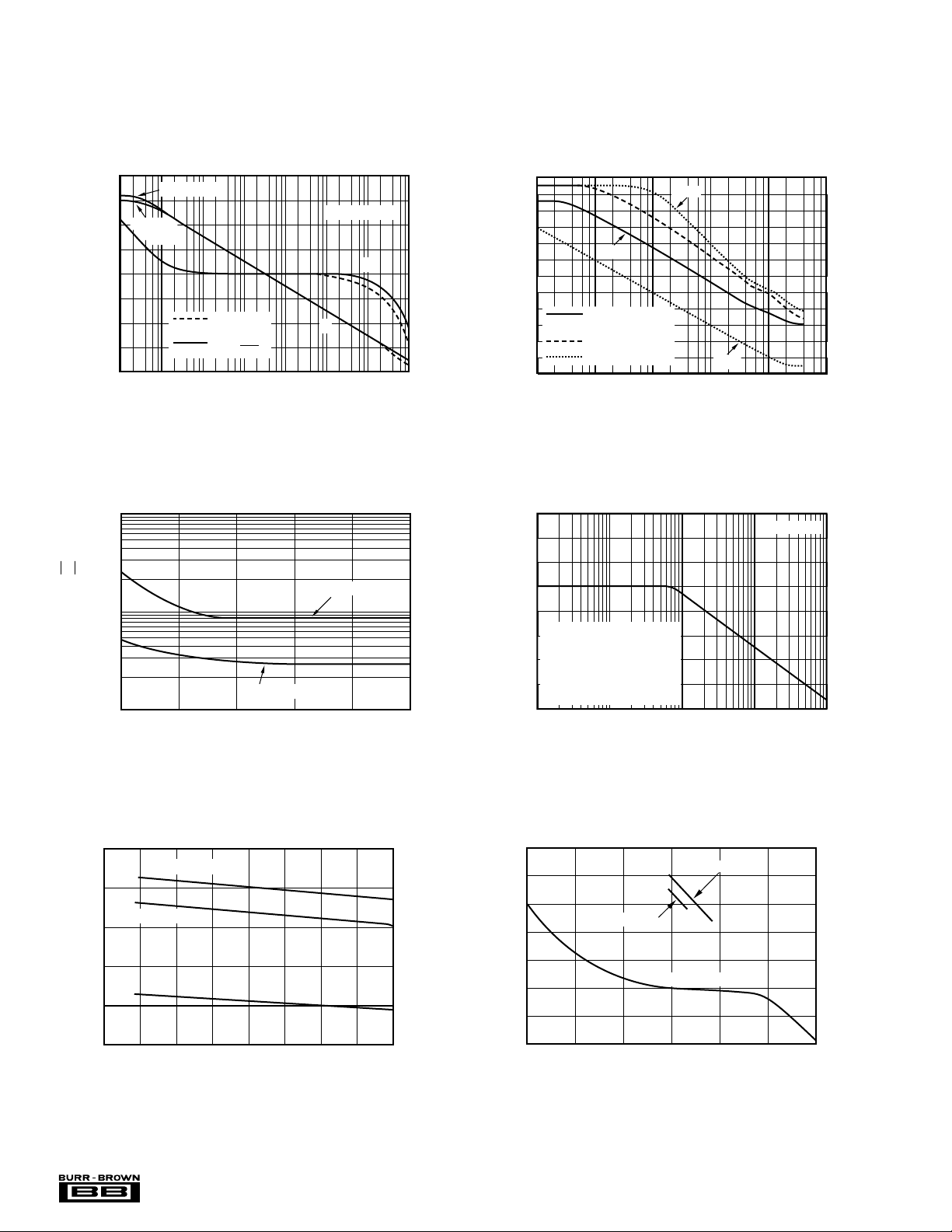
TYPICAL PERFORMANCE CURVES
At TA = +25°C and RL = 10kΩ unless otherwise noted.
140
120
VS = +5V
100
80
60
40
Voltage Gain (dB)
20
0
–20
0.1
1k
100
Current Noise (fA/√Hz)
Voltage Noise (nV/√Hz)
10
1
OPEN-LOOP GAIN/PHASE vs FREQUENCY
VS = +2.7V
CL = 100pF
±15V
φ
VO = 0.25V
V
S
VO =
2
1 10 100 1k 10k 100k 1M
Frequency (Hz)
INPUT NOISE AND CURRENT NOISE
SPECTRAL DENSITY vs FREQUENCY
Voltage Noise
10 100 1k 10k 100k
Frequency (Hz)
G
Current Noise
0
–30
–60
–90
–120
–150
–180
120
110
100
90
80
70
60
Phase (°)
50
40
PSR, CMR (dB)
30
20
10
0
160
140
120
100
Channel Separation (dB)
80
POWER SUPPLY AND COMMON-MODE REJECTION
VS = +2.7V, +5V
or ±15V
V
S
V
S
10 100 1k 10k 100k 1M
CHANNEL SEPARATION vs FREQUENCY
Dual and quad devices.
G = 1, all channels.
Quad measured channel
A to D or B to C—other
combinations yield improved
rejection.
10 100 1k 10k 100k
vs FREQUENCY
CMR
= +2.7V or +5V
= ±15V
Frequency (Hz)
Frequency (Hz)
+PSR
–PSR
RL = 10kΩ
INPUT BIAS AND INPUT OFFSET CURRENT
–20
–15
–10
–5
Input Bias, Input Offset Current (nA)
+5
VS = ±15V
I
OS
0
–75 –50 –25 0 25 50 75 100 125
®
vs TEMPERATURE
VS = +2.7V, +5V
I
B
Ambient Temperature (°C)
OPA234, 2234, 4234
–17
–16
–15
–14
–13
–12
Input Bias Current (nA)
–11
–10
6
INPUT BIAS CURRENT
vs INPUT COMMON-MODE VOLTAGE
VS = +5V
= +2.7V
V
S
VS = ±15V
–15 –10 –5 0 5 10 15
Common-Mode Voltage (V)
Page 7
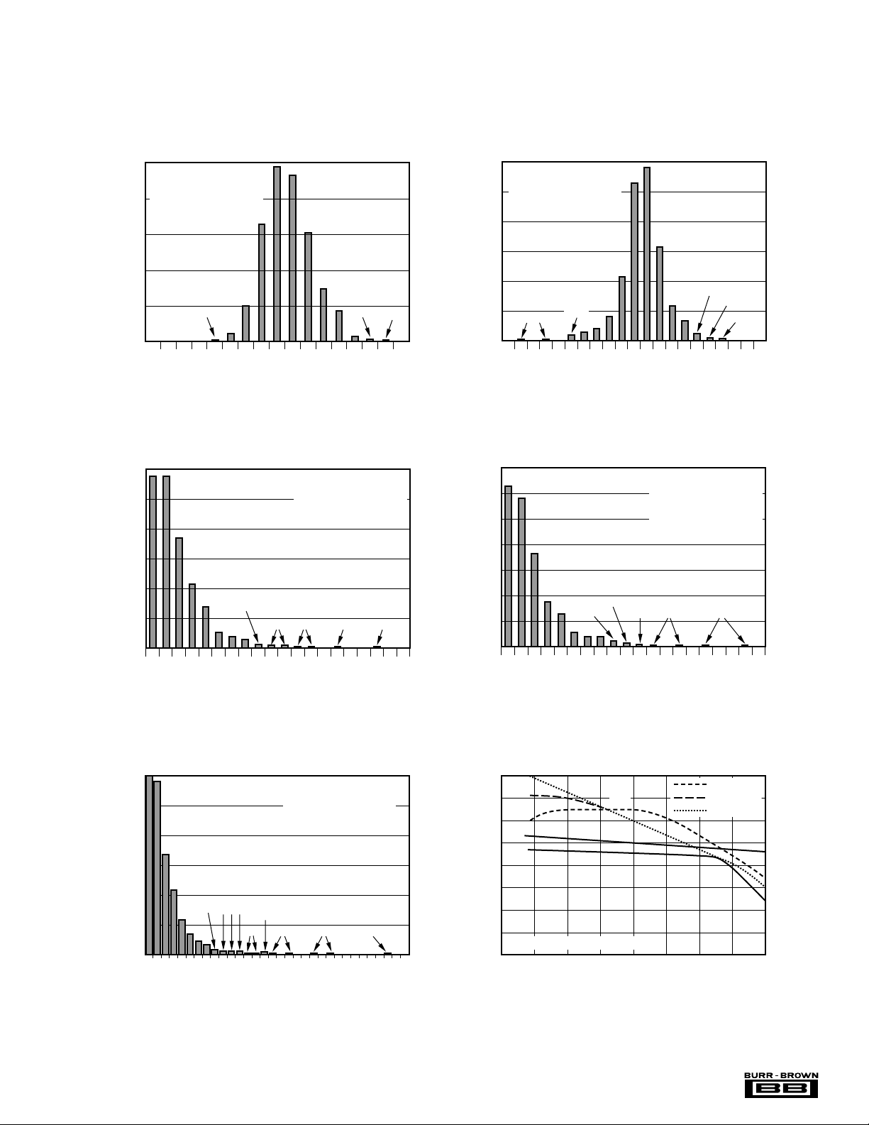
TYPICAL PERFORMANCE CURVES (Cont.)
OFFSET VOLTAGE DRIFT
PRODUCTION DISTRIBUTION
Percent of Amplifiers (%)
Offset Voltage Drift (µV/°C)
3
3.5
4
4.5
5
0.5
1
1.5
2
2.5
35
30
25
20
15
10
5
0
0.1%
0.1%
0.2%
0.5%
0.3%
VS = +5V
Typical production
distribution of packaged
units. Single, dual,
and quad units included.
At TA = +25°C and RL = 10kΩ unless otherwise noted.
25
Typical production
distribution of packaged
20
units. Single, dual, and
quad units included.
15
10
5
Percent of Amplifiers (%)
0
200
35
30
25
20
PRODUCTION DISTRIBUTION
0.1%
175
150
125
PRODUCTION DISTRIBUTION
VS = +2.7V
OFFSET VOLTAGE
75
100
Offset Voltage (µV)
OFFSET VOLTAGE DRIFT
0
50
25
255075
Typical production
distribution of packaged
units. Single, dual,
and quad units included.
= +2.7V, +5V
V
S
0.3%
125
100
150
0.1%
175
200
30
Typical production
distribution of packaged
25
units. Single, dual,
and quad units included.
20
15
10
Percent of Amplifiers (%)
5
0.1%
0
–500
PRODUCTION DISTRIBUTION
0.5%
–400
–300
OFFSET VOLTAGE
0
–200
–100
Offset Voltage (µV)
100
VS = ±15V
0.7%
0.3%
200
300
0.2%
400
500
15
10
Percent of Amplifiers (%)
5
0
1
0.5
30
25
20
15
10
Percent of Amplifiers (%)
5
0
0.5
0.4%
0.3%
0.1% 0.1%0.2% 0.1%
2
1.5
Offset Voltage Drift (µV/°C)
OFFSET VOLTAGE DRIFT
PRODUCTION DISTRIBUTION
VS = ±15V
0.3%
1.5
0.1%
213
2.5
Offset Voltage Drift (µV/°C)
3
2.5
Typical production
distribution of packaged
units. Single, dual,
and quad units included.
0.2%
4
3.5
4.555.566.5
3.5
0.1% 0.1%0.1%
4
4.5
5
140
130
120
110
100
90
, CMR, PSR (dB)
OL
A
80
70
7
8
7.5
60
–75 –50 –25 0 25 50 75 100 125
AOL, CMR, PSR vs TEMPERATURE
A
OL
PSR
CMR
VCM = (V–) –0.02V to (V+) –1V
Ambient Temperature (°C)
VS = +2.7V
= +5V
V
S
= ±15V
V
S
7
OPA234, 2234, 4234
®
Page 8
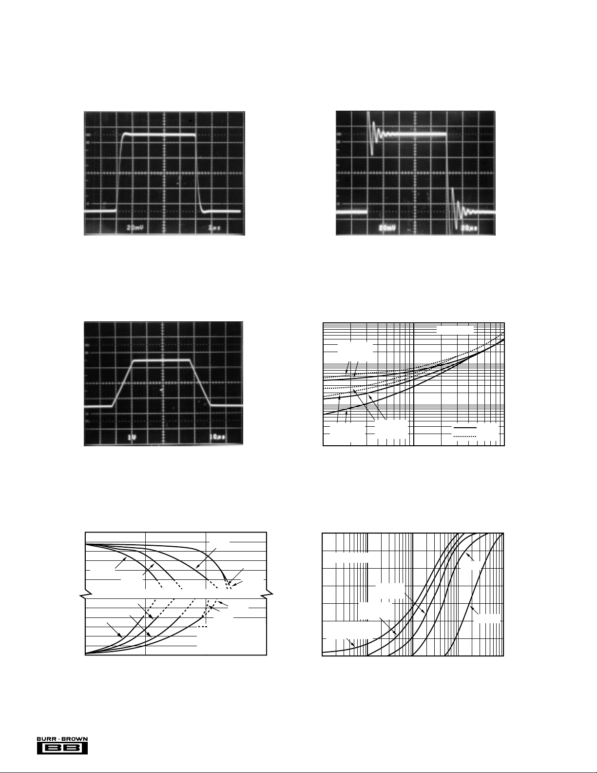
TYPICAL PERFORMANCE CURVES (Cont.)
At TA = +25°C and RL = 10kΩ unless otherwise noted.
20mV/div
SMALL-SIGNAL STEP RESPONSE
G = 1, C
= 100pF, VS = +5V
L
2µs/div
LARGE-SIGNAL STEP RESPONSE
G = 1, C
= 100pF, VS = +5V
L
1000
100
SMALL-SIGNAL STEP RESPONSE
G = 1, C
= 10,000pF, VS = +5V
L
20mV/div
20µs/div
SETTLING TIME vs CLOSED-LOOP GAIN
VS = ±15V,
10V Step
CL = 100pF
1V/div
OUTPUT VOLTAGE SWING vs OUTPUT CURRENT
V+
(V+) –0.5
(V+) –1
(V+) –1.5
(V+) –2
(V+) –2.5
(V+) –3
(V–) +3
(V–) +2.5
(V–) +2
(V–) +1.5
Output Voltage Swing (V)
(V–) +1
(V–) +0.5
125°C
25°C
125°C
V–
0 ±5 ±10
10µs/div
85°C
85°C
Output Current (mA)
25°C
–55°C
–40°C
–40°C
–55°C
High output current may
not be available at low
supply voltages due to
output swing limitations.
±15
10
Settling Time (µs)
VS = +2.7V,
1V Step
1
±1 ±10 ±100
70
60
VO = 100mVp-p
50
40
30
Overshoot (%)
20
10
G = +1,
= +2.7, +5V
V
S
0
10pF 100pF 1nF 10nF 100nF
VS = +5V,
3V Step
Gain (V/V)
SMALL-SIGNAL OVERSHOOT
vs LOAD CAPACITANCE
G = –1,
G = +2
G = +1,
= ±15V
V
S
Load Capacitance
0.1%
0.01%
G = –2
G = ±10
®
OPA234, 2234, 4234
8
Page 9
V+
V–
100kΩ
OPA234 single op amp only.
Use offset adjust pins only to null
offset voltage of op amp—see text.
Trim Range: ±4mV typ
(V–) = 0V for single supply operation.
OPA234
6
7
5
4
3
2
1
10nF
10nF
TYPICAL PERFORMANCE CURVES (Cont.)
At TA = +25°C and RL = 10kΩ unless otherwise noted.
MAXIMUM OUTPUT VOLTAGE
30
25
20
15
10
Output Voltage (Vp-p)
5
0
VS = +5V
VS = ±2.7V
1k
vs FREQUENCY
VS = ±15V
Frequency (Hz)
Maximum output voltage
without slew-rate induced
distortion
10k
100k
APPLICATIONS INFORMATION
OPA234 series op amps are unity-gain stable and suitable
for a wide range of general-purpose applications. Power
supply pins should be bypassed with 10nF ceramic capacitors.
QUIESCENT CURRENT AND SHORT-CIRCUIT CURRENT
525
450
375
300
225
150
Quiescent Current (µA)
75
0
–75 –50 –25 0 25 50 75 100 125
±I
Q
vs TEMPERATURE
Temperature (°C)
VS = +2.7V
V
= +5V
S
V
= +2.7V or +5V
S
V
= ±15V
S
±I
SC
70
60
50
40
30
20
Short-Circuit Current (mA)
10
0
OPERATING VOLTAGE
OPA234 series op amps operate from single (+2.7V to
+36V) or dual (±1.35V to ±18V) supplies with excellent
performance. Specifications are production tested with
+2.7V, +5V, and ±15V supplies. Most behavior remains
unchanged throughout the full operating voltage range.
Parameters which vary significantly with operating voltage are shown in typical performance curves.
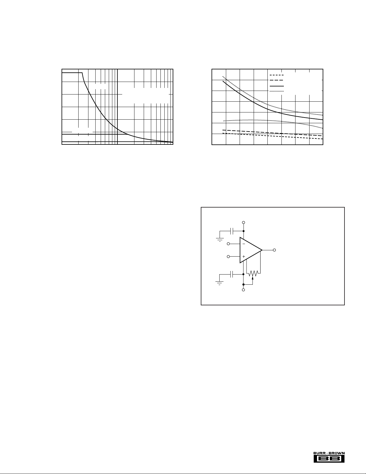
OFFSET VOLTAGE TRIM
Offset voltage of OPA234 series amplifiers is laser trimmed
and usually requires no user adjustment. The OPA234
(single op amp version) provides offset voltage trim connections on pins 1 and 5. Offset voltage can be adjusted by
connecting a potentiometer as shown in Figure 1. This
adjustment should be used only to null the offset of the op
amp, not to adjust system offset or offset produced by the
signal source. Nulling offset could degrade the offset drift
behavior of the op amp. While it is not possible to predict
the exact change in drift, the effect is usually small.
FIGURE 1. OPA234 Offset Voltage Trim Circuit.
9
OPA234, 2234, 4234
®
Page 10

Copyright © Each Manufacturing Company.
All Datasheets cannot be modified without permission.
This datasheet has been download from :
www.AllDataSheet.com
100% Free DataSheet Search Site.
Free Download.
No Register.
Fast Search System.
www.AllDataSheet.com
 Loading...