

Page 1
®
OPA134
OPA134
OPA2134
OPA2134
OPA4134
OPA4134
OPA134
OPA2134
OPA4134
High Performance
TM
AUDIO OPERATIONAL AMPLIFIERS
FEATURES
● SUPERIOR SOUND QUALITY
● ULTRA LOW DISTORTION: 0.00008%
● LOW NOISE: 8nV/√Hz
● TRUE FET-INPUT: I
= 5pA
B
● HIGH SPEED:
SLEW RATE: 20V/µs
BANDWIDTH: 8MHz
● HIGH OPEN-LOOP GAIN: 120dB (600Ω)
● WIDE SUPPLY RANGE:
±2.5V to ±18V
● SINGLE, DUAL, AND QUAD VERSIONS
APPLICATIONS
● PROFESSIONAL AUDIO AND MUSIC
● LINE DRIVERS
● LINE RECEIVERS
● MULTIMEDIA AUDIO
● ACTIVE FILTERS
● PREAMPLIFIERS
● INTEGRATORS
● CROSSOVER NETWORKS
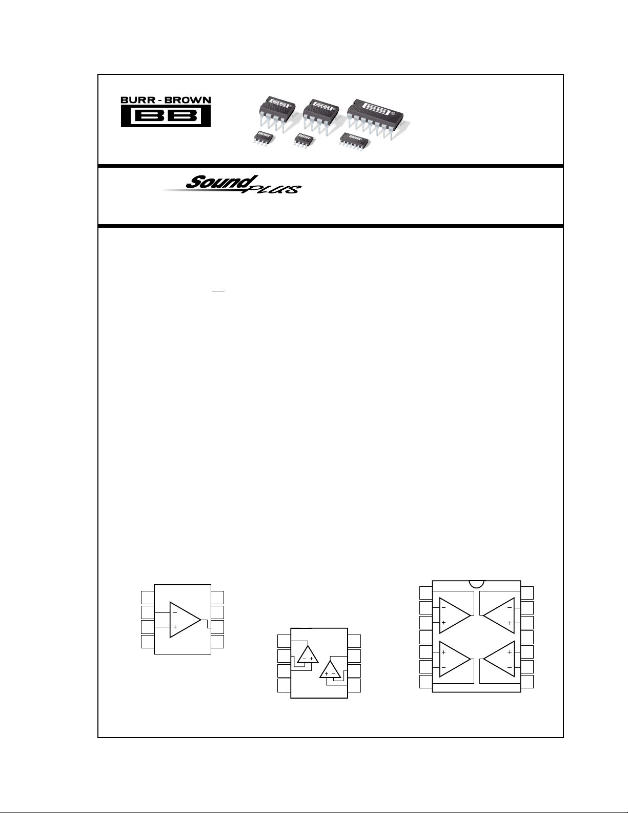
OPA134
Offset Trim
International Airport Industrial Park • Mailing Address: PO Box 11400, Tucson, AZ 85734 • Street Address: 6730 S. Tucson Blvd., Tucson, AZ 85706 • Tel: (520) 746-1111 • Twx: 910-952-1111
1
2
–In
3
+In
4
V–
8-Pin DIP, SO-8
Internet: http://www.burr-brown.com/ • FAXLine: (800) 548-6133 (US/Canada Only) • Cable: BBRCORP • Telex: 066-6491 • FAX: (520) 889-1510 • Immediate Product Info: (800) 548-6132
8
7
6
5
Offset Trim
V+
Output
NC
Out A
–In A
+In A
OPA2134
1
A
2
3
4
V–
8-Pin DIP, SO-8
DESCRIPTION
The OPA134 series are ultra-low distortion, low noise
operational amplifiers fully specified for audio applications. A true FET input stage was incorporated to
provide superior sound quality and speed for exceptional audio performance. This in combination with
high output drive capability and excellent dc performance allows use in a wide variety of demanding
applications. In addition, the OPA134’s wide output
swing, to within 1V of the rails, allows increased
headroom making it ideal for use in any audio circuit.
OPA134 op amps are easy to use and free from phase
inversion and overload problems often found in common FET-input op amps. They can be operated from
±2.5V to ±18V power supplies. Input cascode cir-
cuitry provides excellent common-mode rejection and
maintains low input bias current over its wide input
voltage range, minimizing distortion. OPA134 series
op amps are unity-gain stable and provide excellent
dynamic behavior over a wide range of load conditions, including high load capacitance. The dual and
quad versions feature completely independent circuitry for lowest crosstalk and freedom from interaction, even when overdriven or overloaded.
Single and dual versions are available in 8-pin DIP
and SO-8 surface-mount packages in standard configurations. The quad is available in 14-pin DIP and
SO-14 surface mount packages. All are specified for
–40°C to +85°C operation. A SPICE macromodel is
available for design analysis.
OPA4134
1
Out A
2
–In A
+In A
V+
8
Out B
7
B
–In B
6
+In B
5
V+
+In B
–In B
Out B
AD
3
4
5
BC
6
7
14-Pin DIP
SO-14
Out D
14
–In D
13
+In D
12
V–
11
+In C
10
–In C
9
Out C
8
SBOS058
© 1996 Burr-Brown Corporation PDS-1339C Printed in U.S.A. December, 1997
Page 2
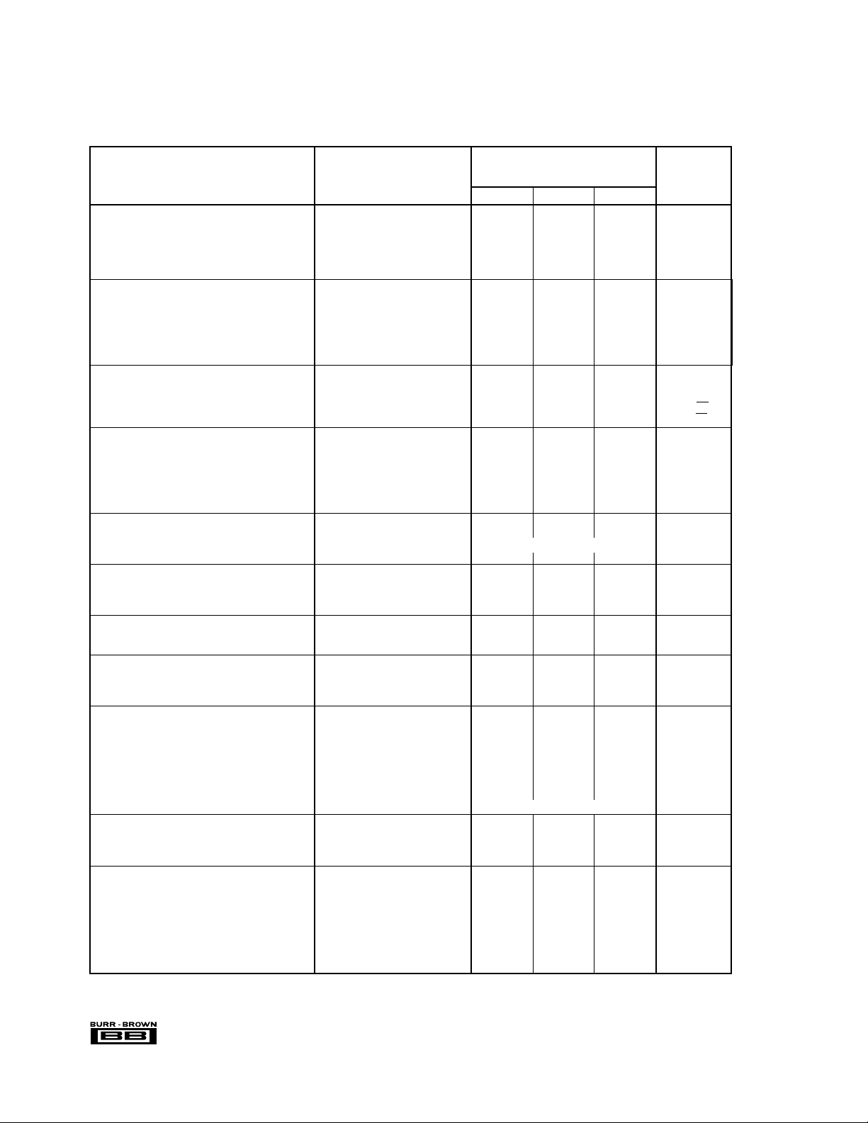
SPECIFICATIONS
At TA = +25°C, VS = ±15V, unless otherwise noted.
OPA134PA, UA
OPA2134PA, UA
OPA4134PA, UA
PARAMETER CONDITION MIN TYP MAX UNITS
AUDIO PERFORMANCE
Total Harmonic Distortion + Noise G = 1, f = 1kHz, V
Intermodulation Distortion G = 1, f = 1kHz, V
(1)
Headroom
THD < 0.01%, RL = 2kΩ, VS = ±18V 23.6 dBu
FREQUENCY RESPONSE
Gain-Bandwidth Product 8 MHz
(2)
Slew Rate
Full Power Bandwidth 1.3 MHz
Settling Time 0.1% G = 1, 10V Step, C
Overload Recovery Time (V
0.01% G = 1, 10V Step, C
IN
NOISE
Input Voltage Noise
Noise Voltage, f = 20Hz to 20kHz 1.2 µVrms
Noise Density, f = 1kHz 8 nV/√Hz
Current Noise Density, f = 1kHz 3 fA/√Hz
OFFSET VOLTAGE
Input Offset Voltage ±0.5 ±2mV
T
= –40°C to +85°C ±1 ±3
vs Temperature T
vs Power Supply (PSRR) V
Channel Separation (Dual, Quad) dc, R
A
= –40°C to +85°C ±2 µV/°C
A
= ±2.5V to ±18V 90 106 dB
S
f = 20kHz, R
INPUT BIAS CURRENT
Input Bias Current
vs Temperature
Input Offset Current
(4)
(3)
(4)
INPUT VOLTAGE RANGE
Common-Mode Voltage Range (V–)+2.5 ±13 (V+)–2.5 V
Common-Mode Rejection V
= –12.5V to +12.5V 86 100 dB
CM
T
= –40°C to +85°C90dB
A
INPUT IMPEDANCE
Differential 10
Common-Mode V
= –12.5V to +12.5V 1013 || 5 Ω || pF
CM
OPEN-LOOP GAIN
Open-Loop Voltage Gain R
= 10kΩ, VO = –14.5V to +13.8V 104 120 dB
L
R
= 2kΩ, VO = –13.8V to +13.5V 104 120 dB
L
R
= 600Ω, VO = –12.8V to +12.5V 104 120 dB
L
OUTPUT
Voltage Output R
Output Current ±35 mA
Output Impedance, Closed-Loop
(5)
Open-Loop f = 10kHz 10 Ω
Short-Circuit Current ±40 mA
Capacitive Load Drive (Stable Operation) See Typical Curve
POWER SUPPLY
Specified Operating Voltage ±15 V
Operating Voltage Range ±2.5 ±18 V
Quiescent Current (per amplifier) I
TEMPERATURE RANGE
Specified Range –40 +85 °C
Operating Range –55 +125 °C
Storage –55 +125 °C
Thermal Resistance,
8-Pin DIP 100 °C/W
θ
JA
SO-8 Surface-Mount 150 °C/W
14-Pin DIP 80 °C/W
SO-14 Surface-Mount 110 °C/W
NOTES: (1) dBu = 20*log (Vrms/0.7746) where Vrms is the maximum output voltage for which THD+Noise is less than 0.01%. See THD+Noise text. (2) Guaranteed
by design. (3) Guaranteed by wafer-level test to 95% confidence level. (4) High-speed test at T
typical curve.
®
OPA134/2134/4134
= 3Vrms
O
R
= 2kΩ 0.00008 %
L
R
= 600Ω 0.00015 %
L
= 1Vp-p –98 dB
O
±15 ±20 V/µs
= 100pF 0.7 µs
L
= 100pF 1 µs
L
) • (Gain) = V
S
= 2kΩ 135 dB
L
= 2kΩ 130 dB
L
0.5 µs
(3)
VCM =0V +5 ±100 pA
See Typical Curve ±5nA
VCM =0V ±2 ±50 pA
13
|| 2 Ω || pF
= 10kΩ (V–)+0.5 (V+)–1.2 V
L
R
= 2kΩ (V–)+1.2 (V+)–1.5 V
L
R
= 600Ω (V–)+2.2 (V+)–2.5 V
L
f = 10kHz 0.01 Ω
= 0 4 5 mA
O
= 25°C. (5) See “Closed-Loop Output Impedance vs Frequency”
J
2
mV
Page 3
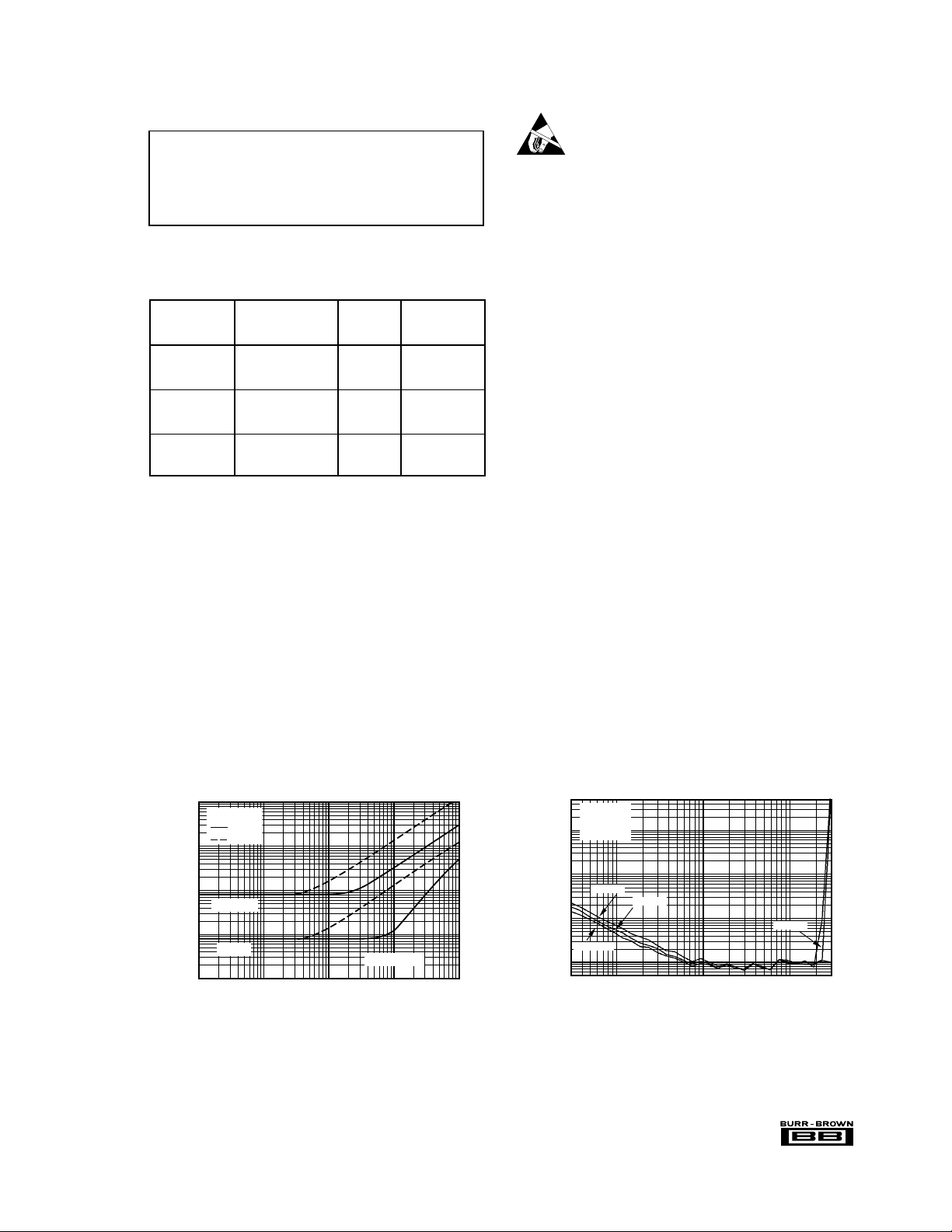
ABSOLUTE MAXIMUM RATINGS
Supply Voltage, V+ to V– .................................................................... 36V
Input Voltage .................................................... (V–) –0.7V to (V+) +0.7V
Output Short-Circuit
Operating Temperature ................................................. –40°C to +125°C
Storage Temperature ..................................................... –55°C to +125°C
Junction Temperature ...................................................................... 150° C
Lead Temperature (soldering, 10s)................................................. 300°C
NOTES: (1) Stresses above these ratings may cause permanent damage.
(2) Short-circuit to ground, one amplifier per package.
(2)
.............................................................. Continuous
(1)
PACKAGE/ORDERING INFORMATION
PACKAGE
DRAWING TEMPERATURE
PRODUCT PACKAGE NUMBER
Single
OPA134PA 8-Pin Plastic DIP 006 –40°C to +85°C
OPA134UA SO-8 Surface-Mount 182 –40°C to +85°C
Dual
OPA2134PA 8-Pin Plastic DIP 006 –40°C to +85°C
OPA2134UA SO-8 Surface-Mount 182 –40°C to +85°C
Quad
OPA4134PA 14-Pin Plastic DIP 010 –40°C to +85°C
OPA4134UA SO-14 Surface-Mount 235 –40°C to +85°C
NOTE: (1) For detailed drawing and dimension table, please see end of data
sheet, or Appendix C of Burr-Brown IC Data Book.
(1)
RANGE
ELECTROSTATIC
DISCHARGE SENSITIVITY
This integrated circuit can be damaged by ESD. Burr-Brown
recommends that all integrated circuits be handled with
appropriate precautions. Failure to observe proper handling
and installation procedures can cause damage.
ESD damage can range from subtle performance degradation to complete device failure. Precision integrated circuits
may be more susceptible to damage because very small
parametric changes could cause the device not to meet its
published specifications.
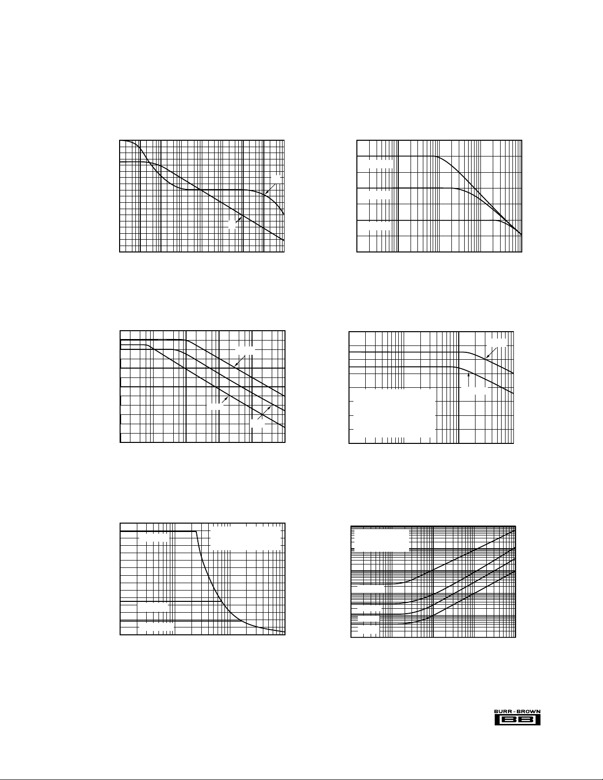
TYPICAL PERFORMANCE CURVES
At TA = +25°C, VS = ±15V, RL = 2kΩ, unless otherwise noted.
TOTAL HARMONIC DISTORTION + NOISE
0.1
0.01
0.001
THD+Noise (%)
0.0001
0.00001
The information provided herein is believed to be reliable; however, BURR-BROWN assumes no responsibility for inaccuracies or omissions. BURR-BROWN assumes
no responsibility for the use of this information, and all use of such information shall be entirely at the user’s own risk. Prices and specifications are subject to change
without notice. No patent rights or licenses to any of the circuits described herein are implied or granted to any third party. BURR-BROWN does not authorize or warrant
any BURR-BROWN product for use in life support devices and/or systems.
R
L
2kΩ
600Ω
G = +10
G = +1
10 100 1k 10k 100k
vs FREQUENCY
Frequency (Hz)
VO = 3Vrms
0.1
IMD (%)
0.010
0.001
0.0005
3 OPA134/2134/4134
SMPTE INTERMODULATION DISTORTION
5
1
30m
G = +1
f = 1kHz
= 2kΩ
R
L
OPA134
Baseline
vs OUTPUT AMPLITUDE
OP176
0.1 1
Output Amplitude (Vpp)
OPA134
10 30
®
Page 4
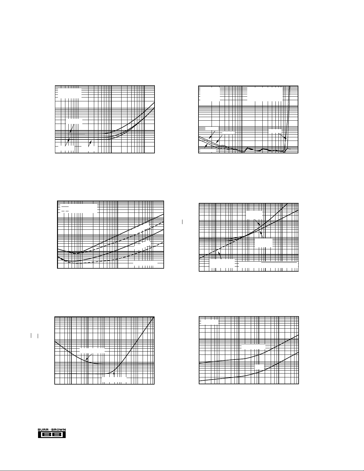
HEADROOM – TOTAL HARMONIC DISTORTION
+ NOISE vs OUTPUT AMPLITUDE
Output Amplitude (Vrms)
THD+Noise (%)
1
0.1
0.010
0.001
0.0005
0.1
1
10 20
VS = ±18V
R
L
= 2kΩ
f = 1kHz
THD < 0.01%
OPA134 – 11.7Vrms
OP176 – 11.1Vrms
Baseline
OP176
OPA134
OPA134
TYPICAL PERFORMANCE CURVES (CONT)
At TA = +25°C, VS = ±15V, RL = 2kΩ, unless otherwise noted.
TOTAL HARMONIC DISTORTION + NOISE
0.01
VO = 10Vrms
= 2kΩ
R
L
0.001
VS = ±16
0.0001
THD+Noise (%)
0.00001
0.00001
VS = ±17
20 100 1k 10k 20k
HARMONIC DISTORTION + NOISE vs FREQUENCY
0.01
2nd Harmonic
3rd Harmonic
0.001
0.0001
vs FREQUENCY
VS = ±18
Frequency (Hz)
Amplitude (% of Fundamentals)
0.000001
20 100 1k 10k 20k
Frequency (Hz)
= 600Ω
L
R
= 2kΩ
L
R
VO = 1Vrms
VOLTAGE NOISE vs SOURCE RESISTANCE
1k
OP176+
100
10
Resistor
OPA134+
Resistor
1
Voltage Noise (nV/√Hz)
Resistor Noise
Only
Vn (total) = √(inRS)2 + e
0.1
10 100 1k 10k 100k 1M 10M
Source Resistance (Ω)
2
+ 4kTR
n
S
INPUT VOLTAGE AND CURRENT NOISE
1k
100
10
Current Noise (fA/√Hz)
Voltage Noise (nV/√Hz)
1
SPECTRAL DENSITY vs FREQUENCY
Voltage Noise
10 100 1k 10k 100k 1M
1
®
Frequency (Hz)
OPA134/2134/4134
Current Noise
INPUT-REFERRED NOISE VOLTAGE
100
RS = 20Ω
10
1
Noise Voltage (µV)
0.1
1 10 100 1k 10k 100k
vs NOISE BANDWIDTH
Peak-to-Peak
RMS
Noise Bandwidth (Hz)
4
Page 5
TYPICAL PERFORMANCE CURVES (CONT)
At TA = +25°C, VS = ±15V, RL = 2kΩ, unless otherwise noted.
160
140
120
100
80
60
40
Voltage Gain (dB)
20
–20
120
100
80
60
40
PSR, CMR (dB)
20
OPEN-LOOP GAIN/PHASE vs FREQUENCY
G
0
0.1 1 10 100 1k 10k 100k 1M 10M
Frequency (Hz)
POWER SUPPLY AND COMMON-MODE REJECTION
vs FREQUENCY
–PSR
+PSR
0
10 100 1k 10k 100k 1M
Frequency (Hz)
CMR
0
–45
φ
–90
–135
Phase Shift (°)
–180
50
40
30
20
10
0
Closed-Loop Gain (dB)
–10
–20
1k 10k 100k 1M 10M
160
140
120
Dual and quad devices.
G = 1, all channels.
Quad measured channel
100
A to D or B to C—other
Channel Separation (dB)
combinations yield improved
rejection.
80
100 1k 10k 100k
CLOSED-LOOP GAIN vs FREQUENCY
G = +100
G = +10
G = +1
Frequency (Hz)
CHANNEL SEPARATION vs FREQUENCY
RL = ∞
RL = 2kΩ
Frequency (Hz)
MAXIMUM OUTPUT VOLTAGE
30
VS = ±15V
20
10
Output Voltage (Vp-p)
VS = ±5V
0
VS = ±2.5V
10k 100k 1M 10M
vs FREQUENCY
Maximum output voltage
without slew-rate
induced distortion
Frequency (Hz)
CLOSED-LOOP OUTPUT IMPEDANCE vs FREQUENCY
10
Note: Open-Loop
Output Impedance
1
at f = 10kHz is 10Ω
0.1
G = +100
0.01
G = +10
0.001
G = +2
Closed-Loop Output Impedance (Ω)
0.0001
G = +1
10 100 1k 10k 100k
Frequency (Hz)
5 OPA134/2134/4134
®
Page 6

TYPICAL PERFORMANCE CURVES (CONT)
At TA = +25°C, VS = ±15V, RL = 2kΩ, unless otherwise noted.
100k
10k
1k
100
10
Input Bias Current (pA)
0.1
150
140
130
120
Open-Loop Gain (dB)
110
INPUT BIAS CURRENT vs TEMPERATURE
High Speed Test
Warmed Up
Dual
1
Single
–75 –50 –25 0 25 50 75 100 125
Ambient Temperature (°C)
OPEN-LOOP GAIN vs TEMPERATURE
RL = 600Ω
RL = 2kΩ
FPO
RL = 10kΩ
INPUT BIAS CURRENT
10
9
8
7
6
5
4
3
Input Bias Current (pA)
2
1
0
–15 –10 –5 0 5 10 15
120
110
100
CMR, PSR (dB)
vs INPUT COMMON-MODE VOLTAGE
High Speed Test
Common-Mode Voltage (V)
CMR, PSR vs TEMPERATURE
PSR
CMR
100
–75 –50 –25 0 25 50 75 100 125
Temperature (°C)
QUIESCENT CURRENT AND SHORT-CIRCUIT CURRENT
4.3
4.2
4.1
4.0
3.9
Quiescent Current Per Amp (mA)
3.8
–75 –50 –25 0 25 50 75 100 125
®
vs TEMPERATURE
±I
Q
Ambient Temperature (°C)
OPA134/2134/4134
90
–75 –50 –25 0 25 50 75 100 125
Ambient Temperature (°C)
60
50
±I
SC
40
30
Short-Circuit Current (mA)
20
10
Output Voltage Swing (V)
OUTPUT VOLTAGE SWING vs OUTPUT CURRENT
15
VIN = 15V
14
13
12
11
10
–10
–11
–12
–13
–14
–15
0 102030405060
125°C
85°C
125°C
VIN = –15V
Output Current (mA)
85°C
–55°C
25°C
25°C25°C
–55°C
6
Page 7

TYPICAL PERFORMANCE CURVES (CONT)
At TA = +25°C, VS = ±15V, RL = 2kΩ, unless otherwise noted.
OFFSET VOLTAGE PRODUCTION DISTRIBUTION
18
16
14
12
10
8
6
4
Percent of Amplifiers (%)
2
0
–2000
–1800
–1600
50mV/div
–800
–1400
–1200
–1000
SMALL-SIGNAL STEP RESPONSE
0
–400
–200
= 100pF
L
200
–600
Offset Voltage (V)
G =1, C
Typical production
distribution of packaged
units.
400
600
800
1000
1200
1400
1600
1800
2000
12
10
8
6
4
Percent of Amplifiers (%)
2
0
0.5
5V/div
PRODUCTION DISTRIBUTION
1.5
2.5
3.5
LARGE-SIGNAL STEP RESPONSE
OFFSET VOLTAGE DRIFT
Typical production
distribution of packaged
units.
4.5
5.5
6.5
7.5
8.5
Offset Voltage Drift (µV/°C)
= 100pF
G = 1, C
L
9.5
10.5
11.5
12.5
200ns/div
100
10
1
Settling Time (µs)
0.1
SETTLING TIME vs CLOSED-LOOP GAIN
0.01%
0.1%
±1 ±10 ±100 ±1000
Closed-Loop Gain (V/V)
1µs/div
SMALL-SIGNAL OVERSHOOT
60
50
G = +1
40
30
Overshoot (%)
20
10
0
100pF 1nF 10nF
vs LOAD CAPACITANCE
G = –1
G = ±10
Load Capacitance
7 OPA134/2134/4134
®
Page 8

APPLICATIONS INFORMATION
OPA134 series op amps are unity-gain stable and suitable
for a wide range of audio and general-purpose applications.
All circuitry is completely independent in the dual version,
assuring normal behavior when one amplifier in a package
is overdriven or short-circuited. Power supply pins should
be bypassed with 10nF ceramic capacitors or larger to
minimize power supply noise.
OPERATING VOLTAGE
OPA134 series op amps operate with power supplies from
±2.5V to ±18V with excellent performance. Although
specifications are production tested with ±15V supplies,
most behavior remains unchanged throughout the full
operating voltage range. Parameters which vary significantly with operating voltage are shown in the typical
performance curves.
OFFSET VOLTAGE TRIM
Offset voltage of OPA134 series amplifiers is laser trimmed
and usually requires no user adjustment. The OPA134
(single op amp version) provides offset trim connections
on pins 1 and 8, identical to 5534 amplifiers. Offset
voltage can be adjusted by connecting a potentiometer as
shown in Figure 1. This adjustment should be used only to
null the offset of the op amp, not to adjust system offset or
offset produced by the signal source. Nulling offset could
change the offset voltage drift behavior of the op amp.
While it is not possible to predict the exact change in drift,
the effect is usually small.
TOTAL HARMONIC DISTORTION
OPA134 series op amps have excellent distortion characteristics. THD+Noise is below 0.0004% throughout the audio
frequency range, 20Hz to 20kHz, with a 2kΩ load. In
addition, distortion remains relatively flat through its
wide output voltage swing range, providing increased headroom compared to other audio amplifiers, including the
OP176/275.
V+
Trim Range: ±4mV typ
10nF
100kΩ
7
1
10nF
2
OPA134
3
V–
8
6
4
OPA134 single op amp only.
Use offset adjust pins only to null
offset voltage of op amp—see text.
FIGURE 1. OPA134 Offset Voltage Trim Circuit.
In many ways headroom is a subjective measurement. It can
be thought of as the maximum output amplitude allowed
while still maintaining a very low level of distortion. In an
attempt to quantify headroom, we have defined “very low
distortion” as 0.01%. Headroom is expressed as a ratio
which compares the maximum allowable output voltage
level to a standard output level (1mW into 600Ω, or
0.7746Vrms). Therefore, OPA134 series op amps, which
have a maximum allowable output voltage level of 11.7Vrms
(THD+Noise < 0.01%), have a headroom specification of
23.6dBu. See the typical curve “Headroom - Total Harmonic
Distortion + Noise vs Output Amplitude.”
DISTORTION MEASUREMENTS
The distortion produced by OPA134 series op amps is below
the measurement limit of all known commercially available
equipment. However, a special test circuit can be used to
extend the measurement capabilities.
Op amp distortion can be considered an internal error source
which can be referred to the input. Figure 2 shows a
circuit which causes the op amp distortion to be 101 times
greater than normally produced by the op amp. The addition
of R
to the otherwise standard non-inverting amplifier
3
R
Signal Gain = 1+
Distortion Gain = 1+
2
R
1
R
2
R1 II R
3
FIGURE 2. Distortion Test Circuit.
®
OPA134/2134/4134
R
1
R
3
OPA134
Generator
Output
Audio Precision
System One
Analyzer
NOTE: (1) Measurement BW = 80kHz
R
2
SIG.
DIST.
GAIN
101
101
101
R
1R2R3
1kΩ
∞
1kΩ
100Ω
1kΩ
10Ω
IBM PC
Compatible
10Ω
11Ω
∞
or
(1)
Analyzer
Input
VO = 3Vrms
RL
1kΩ
GAIN
1
11
101
8
Page 9

configuration alters the feedback factor or noise gain of the
circuit. The closed-loop gain is unchanged, but the feedback
available for error correction is reduced by a factor of 101,
thus extending the resolution by 101. Note that the input
signal and load applied to the op amp are the same as with
conventional feedback without R3. The value of R3 should
be kept small to minimize its effect on the distortion measurements.
Validity of this technique can be verified by duplicating
measurements at high gain and/or high frequency where the
distortion is within the measurement capability of the test
equipment. Measurements for this data sheet were made
with an Audio Precision distortion/noise analyzer which
greatly simplifies such repetitive measurements. The measurement technique can, however, be performed with manual
distortion measurement instruments.
SOURCE IMPEDANCE AND DISTORTION
For lowest distortion with a source or feedback network
which has an impedance greater than 2kΩ, the impedance
seen by the positive and negative inputs in noninverting
applications should be matched. The p-channel JFETs in the
FET input stage exhibit a varying input capacitance with
applied common-mode input voltage. In inverting configurations the input does not vary with input voltage since the
inverting input is held at virtual ground. However, in
noninverting applications the inputs do vary, and the gateto-source voltage is not constant. The effect is increased
distortion due to the varying capacitance for unmatched
source impedances greater than 2kΩ.
To maintain low distortion, match unbalanced source impedance with appropriate values in the feedback network as
shown in Figure 3. Of course, the unbalanced impedance
may be from gain-setting resistors in the feedback path. If
the parallel combination of R
and R2 is greater than 2kΩ, a
1
matching impedance on the noninverting input should be
used. As always, resistor values should be minimized to
reduce the effects of thermal noise.
R
1
If RS > 2kΩ or R1 II R2 > 2kΩ
= R1 II R
R
S
2
V
IN
R
2
OPA134
V
OUT
NOISE PERFORMANCE
Circuit noise is determined by the thermal noise of external
resistors and op amp noise. Op amp noise is described by
two parameters—noise voltage and noise current. The total
noise is quantified by the equation:
2
V total i R e kTR
()( )=++
nnSns
2
4
With low source impedance, the current noise term is
insignificant and voltage noise dominates the noise performance. At high source impedance, the current noise term
becomes the dominant contributor.
Low noise bipolar op amps such as the OPA27 and OPA37
provide very low voltage noise at the expense of a higher
current noise. However, OPA134 series op amps are unique
in providing very low voltage noise and very low current
noise. This provides optimum noise performance over a
wide range of sources, including reactive source impedances, refer to the typical curve, “Voltage Noise vs Source
Resistance.” Above 2kΩ source resistance, the op amp
contributes little additional noise—the voltage and current
terms in the total noise equation become insignificant and
the source resistance term dominates. Below 2kΩ, op amp
voltage noise dominates over the resistor noise, but compares favorably with other audio op amps such as OP176.
PHASE REVERSAL PROTECTION
OPA134 series op amps are free from output phase-reversal
problems. Many audio op amps, such as OP176, exhibit
phase-reversal of the output when the input common-mode
voltage range is exceeded. This can occur in voltage-follower circuits, causing serious problems in control loop
applications. OPA134 series op amps are free from this
undesirable behavior even with inputs of 10V beyond the
input common-mode range.
POWER DISSIPATION
OPA134 series op amps are capable of driving 600Ω loads
with power supply voltage up to ±18V. Internal power
dissipation is increased when operating at high supply
voltages. Copper leadframe construction used in OPA134
series op amps improves heat dissipation compared to conventional materials. Circuit board layout can also help
minimize junction temperature rise. Wide copper traces help
dissipate the heat by acting as an additional heat sink.
Temperature rise can be further minimized by soldering the
devices to the circuit board rather than using a socket.
OUTPUT CURRENT LIMIT
Output current is limited by internal circuitry to approximately ±40mA at 25°C. The limit current decreases with
increasing temperature as shown in the typical performance
curve “Short-Circuit Current vs Temperature.”
FIGURE 3. Impedance Matching for Maintaining Low
Distortion in Non-Inverting Circuits.
®
9 OPA134/2134/4134
Page 10

PACKAGE OPTION ADDENDUM
www.ti.com
22-Oct-2007
PACKAGING INFORMATION
Orderable Device Status
OPA134PA ACTIVE PDIP P 8 50 Green (RoHS &
OPA134PA3 OBSOLETE PDIP P 8 TBD Call TI Call TI
OPA134PAG4 ACTIVE PDIP P 8 50 Green (RoHS &
OPA134UA ACTIVE SOIC D 8 100 Green (RoHS &
OPA134UA/2K5 ACTIVE SOIC D 8 2500 Green (RoHS &
OPA134UA/2K5E4 ACTIVE SOIC D 8 2500 Green (RoHS &
OPA134UA3 OBSOLETE PDIP P 8 TBD Call TI Call TI
OPA134UAE4 ACTIVE SOIC D 8 100 Green (RoHS &
OPA134UAG4 ACTIVE SOIC D 8 100 Green (RoHS &
OPA2134PA ACTIVE PDIP P 8 50 Green (RoHS &
OPA2134PAG4 ACTIVE PDIP P 8 50 Green (RoHS &
OPA2134UA ACTIVE SOIC D 8 100 Green (RoHS &
OPA2134UA/2K5 ACTIVE SOIC D 8 2500 Green (RoHS &
OPA2134UA/2K5E4 ACTIVE SOIC D 8 2500 Green (RoHS &
OPA2134UAE4 ACTIVE SOIC D 8 100 Green (RoHS &
OPA2134UAG4 ACTIVE SOIC D 8 100 Green (RoHS &
OPA4134PA OBSOLETE PDIP N 14 TBD Call TI Call TI
OPA4134UA ACTIVE SOIC D 14 58 Green (RoHS &
OPA4134UA/2K5 ACTIVE SOIC D 14 2500 Green (RoHS &
OPA4134UA/2K5E4 ACTIVE SOIC D 14 2500 Green (RoHS &
OPA4134UAE4 ACTIVE SOIC D 14 58 Green (RoHS &
SN412008DRE4 ACTIVE SOIC D 8 2500 Green (RoHS &
(1)
The marketing status values are defined as follows:
ACTIVE: Product device recommended for new designs.
LIFEBUY: TI has announced that the device will be discontinued, and a lifetime-buy period is in effect.
NRND: Not recommended for new designs. Device is in production to support existing customers, but TI does not recommend using this part in
a new design.
PREVIEW: Device has been announced but is not in production. Samples may or may not be available.
OBSOLETE: TI has discontinued the production of the device.
(1)
Package
Type
Package
Drawing
Pins Package
Qty
Eco Plan
no Sb/Br)
no Sb/Br)
no Sb/Br)
no Sb/Br)
no Sb/Br)
no Sb/Br)
no Sb/Br)
no Sb/Br)
no Sb/Br)
no Sb/Br)
no Sb/Br)
no Sb/Br)
no Sb/Br)
no Sb/Br)
no Sb/Br)
no Sb/Br)
no Sb/Br)
no Sb/Br)
no Sb/Br)
(2)
Lead/Ball Finish MSL Peak Temp
CU NIPDAU N / A for Pkg Type
CU NIPDAU N / A for Pkg Type
CU NIPDAU Level-3-260C-168 HR
CU NIPDAU Level-3-260C-168 HR
CU NIPDAU Level-3-260C-168 HR
CU NIPDAU Level-3-260C-168 HR
CU NIPDAU Level-3-260C-168 HR
CU NIPDAU N / A for Pkg Type
CU NIPDAU N / A for Pkg Type
CU NIPDAU Level-3-260C-168 HR
CU NIPDAU Level-3-260C-168 HR
CU NIPDAU Level-3-260C-168 HR
CU NIPDAU Level-3-260C-168 HR
CU NIPDAU Level-3-260C-168 HR
CU NIPDAU Level-3-260C-168 HR
CU NIPDAU Level-3-260C-168 HR
CU NIPDAU Level-3-260C-168 HR
CU NIPDAU Level-3-260C-168 HR
CU NIPDAU Level-3-260C-168 HR
(3)
Addendum-Page 1
Page 11

PACKAGE OPTION ADDENDUM
www.ti.com
(2)
Eco Plan - The planned eco-friendly classification: Pb-Free (RoHS), Pb-Free (RoHS Exempt), or Green (RoHS & no Sb/Br) - please check
http://www.ti.com/productcontent for the latest availability information and additional product content details.
TBD: The Pb-Free/Green conversion plan has not been defined.
Pb-Free (RoHS): TI's terms "Lead-Free" or "Pb-Free" mean semiconductor products that are compatible with the current RoHS requirements
for all 6 substances, including the requirement that lead not exceed 0.1% by weight in homogeneous materials. Where designed to be soldered
at high temperatures, TI Pb-Free products are suitable for use in specified lead-free processes.
Pb-Free (RoHS Exempt): This component has a RoHS exemption for either 1) lead-based flip-chip solder bumps used between the die and
package, or 2) lead-based die adhesive used between the die and leadframe. The component is otherwise considered Pb-Free (RoHS
compatible) as defined above.
Green (RoHS & no Sb/Br): TI defines "Green" to mean Pb-Free (RoHS compatible), and free of Bromine (Br) and Antimony (Sb) based flame
retardants (Br or Sb do not exceed 0.1% by weight in homogeneous material)
(3)
MSL, Peak Temp. -- The Moisture Sensitivity Level rating according to the JEDEC industry standard classifications, and peak solder
temperature.
Important Information and Disclaimer:The information provided on this page represents TI's knowledge and belief as of the date that it is
provided. TI bases its knowledge and belief on information provided by third parties, and makes no representation or warranty as to the
accuracy of such information. Efforts are underway to better integrate information from third parties. TI has taken and continues to take
reasonable steps to provide representative and accurate information but may not have conducted destructive testing or chemical analysis on
incoming materials and chemicals. TI and TI suppliers consider certain information to be proprietary, and thus CAS numbers and other limited
information may not be available for release.
In no event shall TI's liability arising out of such information exceed the total purchase price of the TI part(s) at issue in this document sold by TI
to Customer on an annual basis.
22-Oct-2007
Addendum-Page 2
Page 12

PACKAGE MATERIALS INFORMATION
www.ti.com
TAPE AND REEL INFORMATION
11-Mar-2008
*All dimensions are nominal
Device Package
Type
OPA134UA/2K5 SOIC D 8 2500 330.0 12.4 6.4 5.2 2.1 8.0 12.0 Q1
OPA2134UA/2K5 SOIC D 8 2500 330.0 12.4 6.4 5.2 2.1 8.0 12.0 Q1
OPA4134UA/2K5 SOIC D 14 2500 330.0 16.4 6.5 9.0 2.1 8.0 16.0 Q1
Package
Drawing
Pins SPQ Reel
Diameter
(mm)
Reel
Width
W1 (mm)
A0 (mm) B0 (mm) K0 (mm) P1
(mm)W(mm)
Pin1
Quadrant
Pack Materials-Page 1
Page 13

PACKAGE MATERIALS INFORMATION
www.ti.com
11-Mar-2008
*All dimensions are nominal
Device Package Type Package Drawing Pins SPQ Length (mm) Width (mm) Height (mm)
OPA134UA/2K5 SOIC D 8 2500 346.0 346.0 29.0
OPA2134UA/2K5 SOIC D 8 2500 346.0 346.0 29.0
OPA4134UA/2K5 SOIC D 14 2500 346.0 346.0 33.0
Pack Materials-Page 2
Page 14

IMPORTANT NOTICE
Texas Instruments Incorporated and its subsidiaries (TI) reserve the right to make corrections, modifications, enhancements, improvements,
and other changes to its products and services at any time and to discontinue any product or service without notice. Customers should
obtain the latest relevant information before placing orders and should verify that such information is current and complete. All products are
sold subject to TI’s terms and conditions of sale supplied at the time of order acknowledgment.
TI warrants performance of its hardware products to the specifications applicable at the time of sale in accordance with TI’s standard
warranty. Testing and other quality control techniques are used to the extent TI deems necessary to support this warranty. Except where
mandated by government requirements, testing of all parameters of each product is not necessarily performed.
TI assumes no liability for applications assistance or customer product design. Customers are responsible for their products and
applications using TI components. To minimize the risks associated with customer products and applications, customers should provide
adequate design and operating safeguards.
TI does not warrant or represent that any license, either express or implied, is granted under any TI patent right, copyright, mask work right,
or other TI intellectual property right relating to any combination, machine, or process in which TI products or services are used. Information
published by TI regarding third-party products or services does not constitute a license from TI to use such products or services or a
warranty or endorsement thereof. Use of such information may require a license from a third party under the patents or other intellectual
property of the third party, or a license from TI under the patents or other intellectual property of TI.
Reproduction of TI information in TI data books or data sheets is permissible only if reproduction is without alteration and is accompanied
by all associated warranties, conditions, limitations, and notices. Reproduction of this information with alteration is an unfair and deceptive
business practice. TI is not responsible or liable for such altered documentation. Information of third parties may be subject to additional
restrictions.
Resale of TI products or services with statements different from or beyond the parameters stated by TI for that product or service voids all
express and any implied warranties for the associated TI product or service and is an unfair and deceptive business practice. TI is not
responsible or liable for any such statements.
TI products are not authorized for use in safety-critical applications (such as life support) where a failure of the TI product would reasonably
be expected to cause severe personal injury or death, unless officers of the parties have executed an agreement specifically governing
such use. Buyers represent that they have all necessary expertise in the safety and regulatory ramifications of their applications, and
acknowledge and agree that they are solely responsible for all legal, regulatory and safety-related requirements concerning their products
and any use of TI products in such safety-critical applications, notwithstanding any applications-related information or support that may be
provided by TI. Further, Buyers must fully indemnify TI and its representatives against any damages arising out of the use of TI products in
such safety-critical applications.
TI products are neither designed nor intended for use in military/aerospace applications or environments unless the TI products are
specifically designated by TI as military-grade or "enhanced plastic." Only products designated by TI as military-grade meet military
specifications. Buyers acknowledge and agree that any such use of TI products which TI has not designated as military-grade is solely at
the Buyer's risk, and that they are solely responsible for compliance with all legal and regulatory requirements in connection with such use.
TI products are neither designed nor intended for use in automotive applications or environments unless the specific TI products are
designated by TI as compliant with ISO/TS 16949 requirements. Buyers acknowledge and agree that, if they use any non-designated
products in automotive applications, TI will not be responsible for any failure to meet such requirements.
Following are URLs where you can obtain information on other Texas Instruments products and application solutions:
Products Applications
Amplifiers amplifier.ti.com Audio www.ti.com/audio
Data Converters dataconverter.ti.com Automotive www.ti.com/automotive
DSP dsp.ti.com Broadband www.ti.com/broadband
Clocks and Timers www.ti.com/clocks Digital Control www.ti.com/digitalcontrol
Interface interface.ti.com Medical www.ti.com/medical
Logic logic.ti.com Military www.ti.com/military
Power Mgmt power.ti.com Optical Networking www.ti.com/opticalnetwork
Microcontrollers microcontroller.ti.com Security www.ti.com/security
RFID www.ti-rfid.com Telephony www.ti.com/telephony
RF/IF and ZigBee® Solutions www.ti.com/lprf Video & Imaging www.ti.com/video
Mailing Address: Texas Instruments, Post Office Box 655303, Dallas, Texas 75265
Copyright © 2008, Texas Instruments Incorporated
Wireless www.ti.com/wireless
 Loading...