

Burr Brown OPA2107AP, OPA2107AU, OPA2107AU-2K5 Datasheet
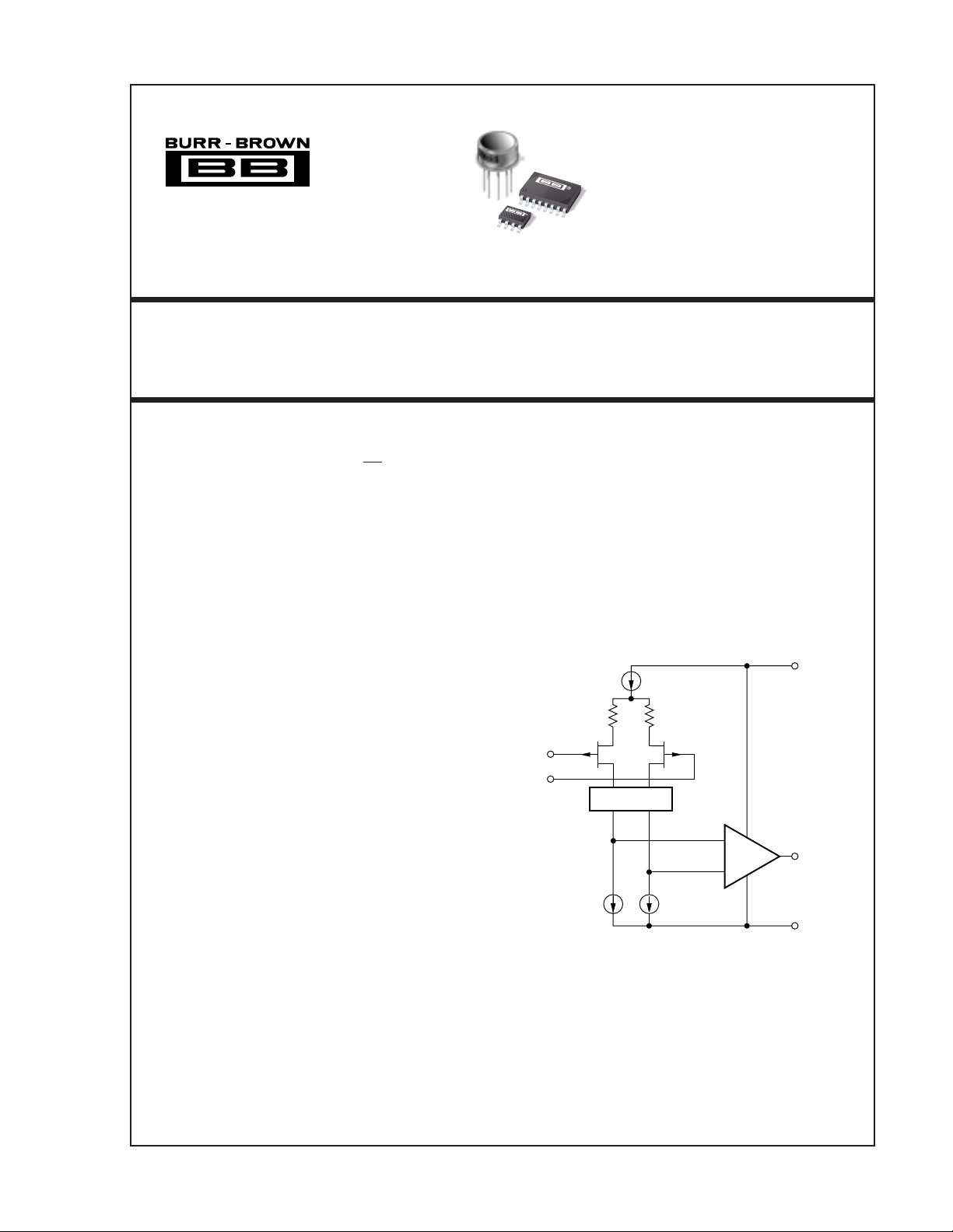
Cascode
–In
(2, 6)
+In
(3, 5)
+V
(8)
S
Output
(1, 7)
–V
(4)
S
®
OPA2107
OPA2107
OPA2107
Precision Dual
OPERATIONAL AMPLIFIER
FEATURES
● VERY LOW NOISE: 8nV/√Hz at 10kHz
● LOW V
● LOW DRIFT: 10µV/
● LOW I
● FAST SETTLING TIME: 2µs to 0.01%
● UNITY-GAIN STABLE
DESCRIPTION
The OPA2107 dual operational amplifier provides
precision
savings of a dual op amp. It is useful in a wide range
of precision and low-noise analog circuitry and can be
used to upgrade the performance of designs currently
using BIFET® type amplifiers.
The OPA2107 is fabricated on a proprietary
dielectrically isolated (
put bias currents to very low levels without sacrificing
other important parameters, such as input offset voltage, drift and noise. Laser-trimmed input circuitry
yields excellent DC performance. Superior dynamic
performance is achieved, yet quiescent current is held
to under 2.5mA per amplifier. The OPA2107 is unitygain stable.
The OPA2107 is available in plastic DIP and SOIC
packages. Industrial temperature range versions are
available.
: 1mV max
OS
°C max
: 10pA max
B
Difet
performance with the cost and space
Difet
) process. This holds in-
Difet
®
APPLICATIONS
● DATA ACQUISITION
● DAC OUTPUT AMPLIFIER
● OPTOELECTRONICS
● HIGH-IMPEDANCE SENSOR AMPS
● HIGH-PERFORMANCE AUDIO CIRCUITRY
● MEDICAL EQUIPMENT, CT SCANNERS
®
Difet
Burr-Brown Corp.
BIFET® National Semiconductor
International Airport Industrial Park • Mailing Address: PO Box 11400, Tucson, AZ 85734 • Street Address: 6730 S. Tucson Blvd., Tucson, AZ 85706 • Tel: (520) 746-1111 • Twx: 910-952-1111
Internet: http://www.burr-brown.com/ • FAXLine: (800) 548-6133 (US/Canada Only) • Cable: BBRCORP • Telex: 066-6491 • FAX: (520) 889-1510 • Immediate Product Info: (800) 548-6132
©
1989 Burr-Brown Corporation PDS-863E Printed in U.S.A. April, 1998
®
1
OPA2107

SPECIFICATIONS
At TA = +25°C, VS = ±15V, unless otherwise noted.
OPA2107AP, AU
PARAMETER CONDITION MIN TYP MAX UNITS
OFFSET VOLTAGE
Input Offset Voltage VCM = 0V 100 1 mV
Over Specified Temperature 0.5 2 mV
Average Drift Over Specified Temperature 310µV/°C
Power Supply Rejection V
INPUT BIAS CURRENT
Input Bias Current VCM = 0V 4 10 pA
Over Specified Temperature 0.25 1.5 nA
Input Offset Current V
Over Specified Temperature 1nA
INPUT NOISE
Voltage: f = 10Hz R
f = 100Hz 12 nV/√Hz
f = 1kHz 9 nV/√Hz
f = 10kHz 8 nV/√Hz
BW = 0.1 to 10Hz 1.2 µVp-p
BW = 10 to 10kHz 0.85 µVrms
Current: f = 0.1Hz thru 20kHz 1.2 fA/√Hz
BW = 0.1Hz to 10Hz 23 fAp-p
INPUT IMPEDANCE
Differential 10
Common-Mode 10
INPUT VOLTAGE RANGE
Common-Mode Input Range ±10.5 ±11 V
Over Specified Temperature ±10.2 ±10.5 V
Common-Mode Rejection V
OPEN-LOOP GAIN
Open-Loop Voltage Gain V
Over Specified Temperature 80 94 dB
DYNAMIC RESPONSE
Slew Rate G = +1 13 18 V/µs
Settling Time: 0.1% G = –1, 10V Step 1.5 µs
Gain Bandwidth Product G = 100 4.5 MHz
THD + Noise G = +1, f = 1kHz 0.001 %
Channel Separation f = 100Hz, R
POWER SUPPLY
Specified Operating Voltage ±15 V
Operating Voltage Range ±4.5 V
Current ±4.5 mA
OUTPUT
Voltage Output R
Over Specified Temperature ±10.5 ±11.5 V
Short Circuit Current ±10 ±40 mA
Output Resistance, Open-Loop 1MHz 70 Ω
Capacitive Load Stability G = +1 1000 pF
TEMPERATURE RANGE
Specification –25 +85 °C
Operating –25 +85 °C
Storage –40 +125 °C
Thermal Resistance (
8-Pin DIP 90 °C/W
8-Lead Surface Mount 175 °C/W
NOTE: (1) Specified with devices fully warmed up.
(1)
= ±10 to ±18V 80 96 dB
(1)
S
= 0V 1 8 pA
CM
= 0 30 nV/√Hz
S
13
|| 2 Ω || pF
14
|| 4 Ω || pF
= ±10V 80 94 dB
CM
= ±10V, RL = 2kΩ 82 96 dB
O
0.01% 2 µs
= 2kΩ 120 dB
L
= 2kΩ±11 ±12 V
L
θ
)
J-A
®
2OPA2107
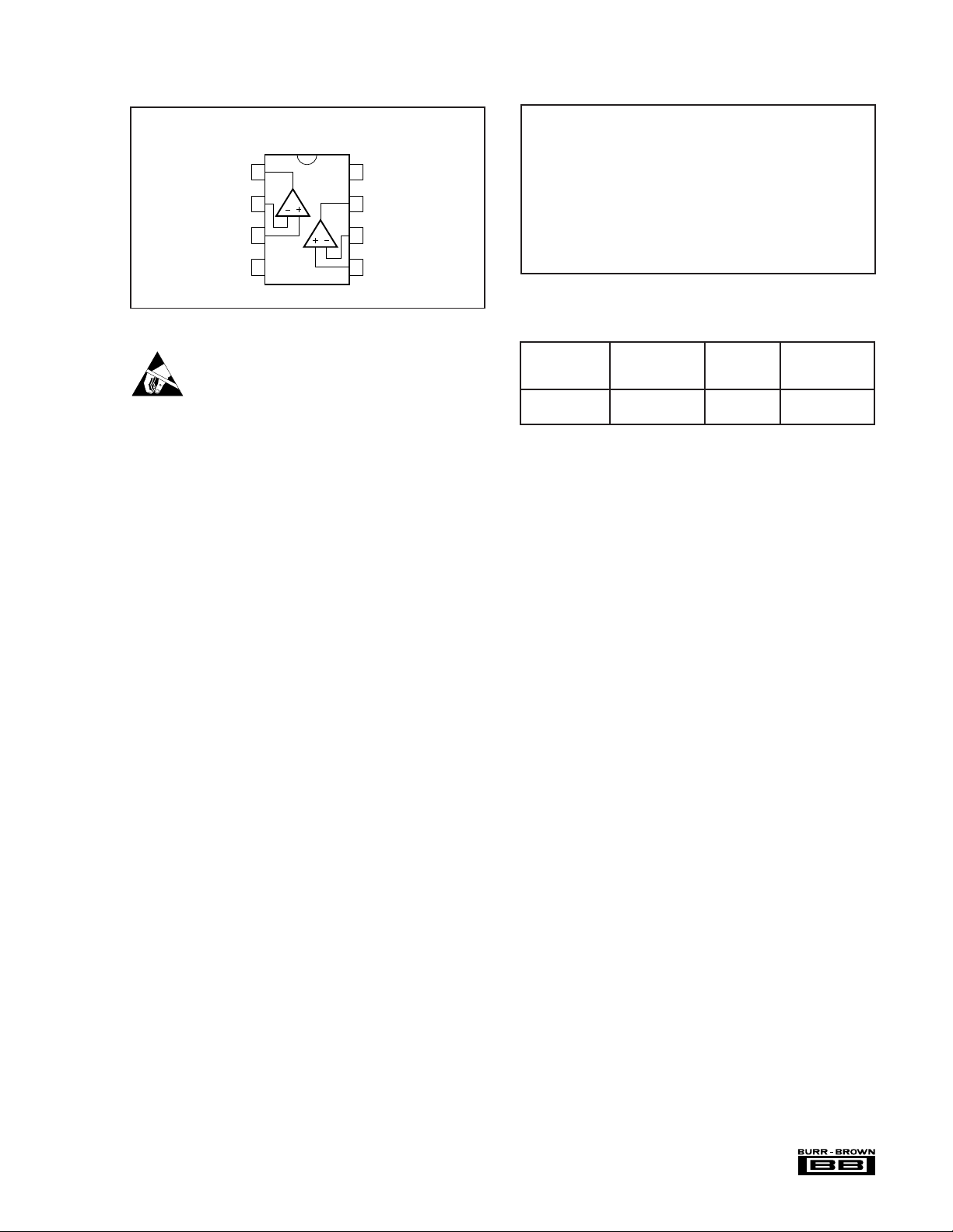
PIN CONFIGURATION
Top View DIP, SOIC
+V
Out A
–In A
+In A
–V
1
A
2
3
4
S
8
S
7
Out B
B
–In B
6
+In B
5
ELECTROSTATIC
DISCHARGE SENSITIVITY
This integrated circuit can be damaged by ESD. Burr-Brown
recommends that all integrated circuits be handled with
appropriate precautions. Failure to observe proper handling
and installation procedures can cause damage.
ESD damage can range from subtle performance degradation
to complete device failure. Precision integrated circuits may
be more susceptible to damage because very small parametric
changes could cause the device not to meet its published
specifications.
ABSOLUTE MAXIMUM RATINGS
Supply Voltage................................................................................... ±18V
Input Voltage Range ..................................................................... ±V
Differential Input Voltage........................................................ Total V
Operating Temperature
P and U Packages ........................................................ –25°C to + 85°C
Storage Temperature
P and U Packages ....................................................... –40°C to +125°C
Output Short Circuit to Ground (T
Junction Temperature .................................................................... +175°C
Lead Temperature
P Package (soldering, 10s) ......................................................... +300°C
U Package, SOIC (3s) ................................................................ +260°C
NOTE: Stresses above these ratings may cause permanent damage.
= +25°C) ........................... Continuous
A
(1)
±2V
S
±4V
S
PACKAGE/ORDERING INFORMATION
PACKAGE
DRAWING TEMPERATURE
PRODUCT PACKAGE NUMBER
OPA2107AP Plastic DIP 006 –25 to +85°C
OPA2107AU SO-8 SOIC 182 –25 to +85°C
NOTE: (1) For detailed drawing and dimension table, please see end of data
sheet, or Appendix C of Burr-Brown IC Data Book.
(1)
RANGE
The information provided herein is believed to be reliable; however, BURR-BROWN assumes no responsibility for inaccuracies or omissions. BURR-BROWN assumes
no responsibility for the use of this information, and all use of such information shall be entirely at the user’s own risk. Prices and specifications are subject to change
without notice. No patent rights or licenses to any of the circuits described herein are implied or granted to any third party. BURR-BROWN does not authorize or warrant
any BURR-BROWN product for use in life support devices and/or systems.
3
OPA2107
®
 Loading...