

Page 1
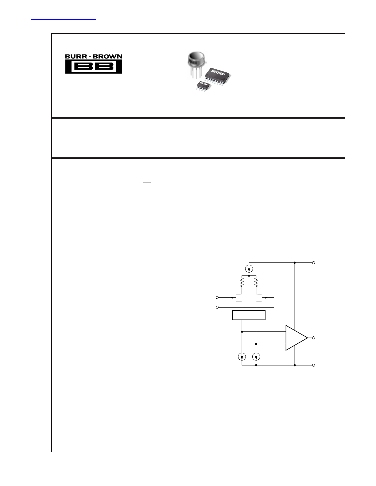
Cascode
–In
(2, 6)
+In
(3, 5)
+V
(8)
S
Output
(1, 7)
–V
(4)
S
查询OPA2107供应商
®
Precision Dual
OPERATIONAL AMPLIFIER
FEATURES
● VERY LOW NOISE: 8nV/√Hz at 10kHz
● LOW V
● LOW DRIFT: 10µV/
● LOW I
● FAST SETTLING TIME: 2µs to 0.01%
● UNITY-GAIN STABLE
: 1mV max
OS
: 10pA max
B
°C max
OPA2107
OPA2107
OPA2107
Difet
APPLICATIONS
● DATA ACQUISITION
● DAC OUTPUT AMPLIFIER
● OPTOELECTRONICS
● HIGH-IMPEDANCE SENSOR AMPS
● HIGH-PERFORMANCE AUDIO CIRCUITRY
● MEDICAL EQUIPMENT, CT SCANNERS
®
DESCRIPTION
The OPA2107 dual operational amplifier provides
Difet
precision
savings of a dual op amp. It is useful in a wide range
of precision and low-noise analog circuitry and can be
used to upgrade the performance of designs currently
using BIFET® type amplifiers.
The OPA2107 is fabricated on a proprietary
dielectrically isolated (
put bias currents to very low levels without sacrificing
other important parameters, such as input offset voltage, drift and noise. Laser-trimmed input circuitry
yields excellent DC performance. Superior dynamic
performance is achieved, yet quiescent current is held
to under 2.5mA per amplifier. The OPA2107 is unitygain stable.
The OPA2107 is available in plastic DIP and SOIC
packages. Industrial temperature range versions are
available.
®
Difet
Burr-Brown Corp.
BIFET® National Semiconductor
International Airport Industrial Park • Mailing Address: PO Box 11400, Tucson, AZ 85734 • Street Address: 6730 S. Tucson Blvd., Tucson, AZ 85706 • Tel: (520) 746-1111 • Twx: 910-952-1111
Internet: http://www.burr-brown.com/ • FAXLine: (800) 548-6133 (US/Canada Only) • Cable: BBRCORP • Telex: 066-6491 • FAX: (520) 889-1510 • Immediate Product Info: (800) 548-6132
©
1989 Burr-Brown Corporation PDS-863E Printed in U.S.A. April, 1998
performance with the cost and space
Difet
) process. This holds in-
®
1
OPA2107
Page 2

SPECIFICATIONS
At TA = +25°C, VS = ±15V, unless otherwise noted.
OPA2107AP, AU
PARAMETER CONDITION MIN TYP MAX UNITS
OFFSET VOLTAGE
Input Offset Voltage VCM = 0V 100 1 mV
Over Specified Temperature 0.5 2 mV
Average Drift Over Specified Temperature 310µV/°C
Power Supply Rejection V
INPUT BIAS CURRENT
Input Bias Current VCM = 0V 4 10 pA
Over Specified Temperature 0.25 1.5 nA
Input Offset Current V
Over Specified Temperature 1nA
INPUT NOISE
Voltage: f = 10Hz R
f = 100Hz 12 nV/√Hz
f = 1kHz 9 nV/√Hz
f = 10kHz 8 nV/√Hz
BW = 0.1 to 10Hz 1.2 µVp-p
BW = 10 to 10kHz 0.85 µVrms
Current: f = 0.1Hz thru 20kHz 1.2 fA/√Hz
BW = 0.1Hz to 10Hz 23 fAp-p
INPUT IMPEDANCE
Differential 10
Common-Mode 10
INPUT VOLTAGE RANGE
Common-Mode Input Range ±10.5 ±11 V
Over Specified Temperature ±10.2 ±10.5 V
Common-Mode Rejection V
OPEN-LOOP GAIN
Open-Loop Voltage Gain V
Over Specified Temperature 80 94 dB
DYNAMIC RESPONSE
Slew Rate G = +1 13 18 V/µs
Settling Time: 0.1% G = –1, 10V Step 1.5 µs
Gain Bandwidth Product G = 100 4.5 MHz
THD + Noise G = +1, f = 1kHz 0.001 %
Channel Separation f = 100Hz, R
POWER SUPPLY
Specified Operating Voltage ±15 V
Operating Voltage Range ±4.5 V
Current ±4.5 mA
OUTPUT
Voltage Output R
Over Specified Temperature ±10.5 ±11.5 V
Short Circuit Current ±10 ±40 mA
Output Resistance, Open-Loop 1MHz 70 Ω
Capacitive Load Stability G = +1 1000 pF
TEMPERATURE RANGE
Specification –25 +85 °C
Operating –25 +85 °C
Storage –40 +125 °C
Thermal Resistance (
8-Pin DIP 90 °C/W
8-Lead Surface Mount 175 °C/W
NOTE: (1) Specified with devices fully warmed up.
(1)
= ±10 to ±18V 80 96 dB
(1)
S
= 0V 1 8 pA
CM
= 0 30 nV/√Hz
S
13
|| 2 Ω || pF
14
|| 4 Ω || pF
= ±10V 80 94 dB
CM
= ±10V, RL = 2kΩ 82 96 dB
O
0.01% 2 µs
= 2kΩ 120 dB
L
= 2kΩ±11 ±12 V
L
θ
)
J-A
®
2OPA2107
Page 3
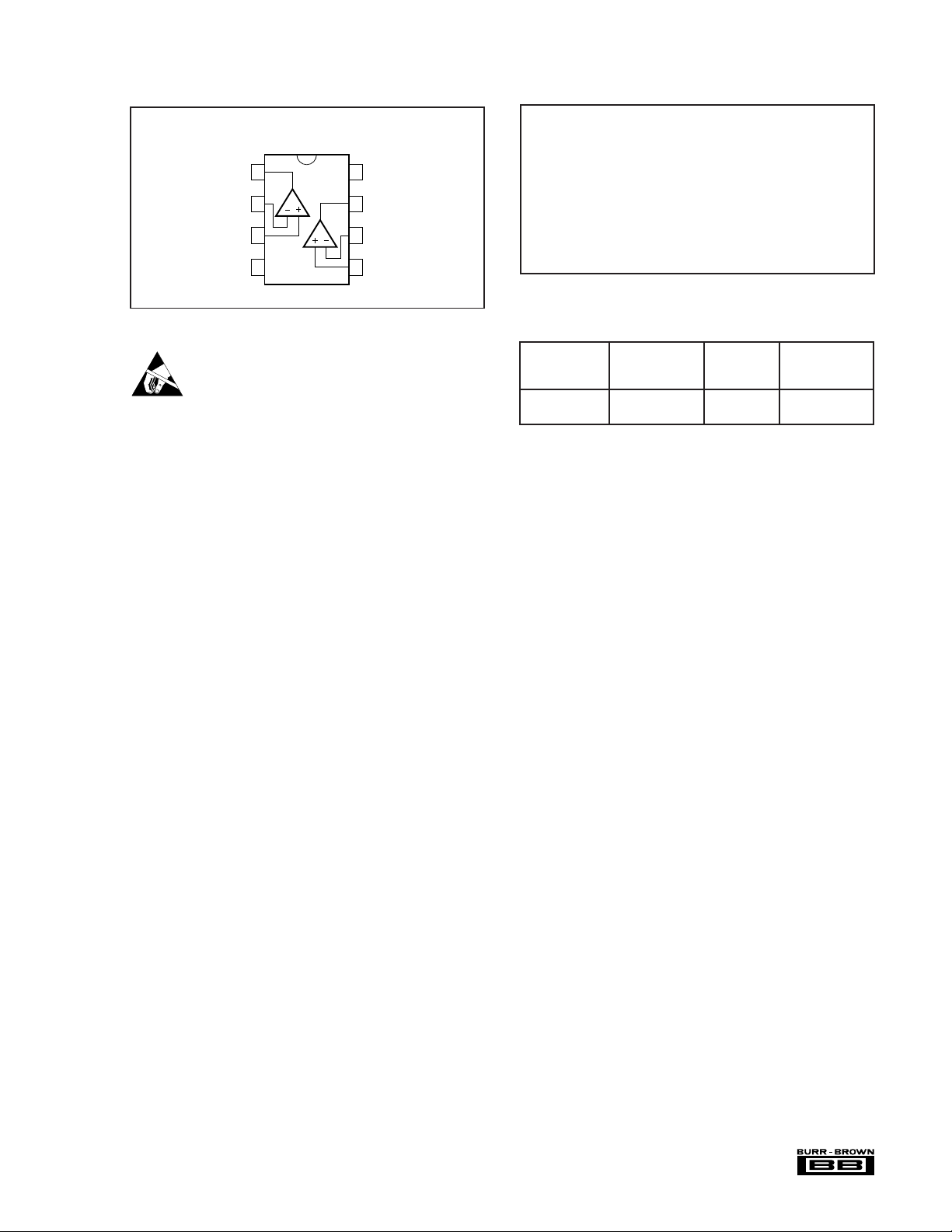
PIN CONFIGURATION
Top View DIP, SOIC
+V
Out A
–In A
+In A
–V
1
A
2
3
4
S
8
S
7
Out B
B
–In B
6
+In B
5
ELECTROSTATIC
DISCHARGE SENSITIVITY
This integrated circuit can be damaged by ESD. Burr-Brown
recommends that all integrated circuits be handled with
appropriate precautions. Failure to observe proper handling
and installation procedures can cause damage.
ESD damage can range from subtle performance degradation
to complete device failure. Precision integrated circuits may
be more susceptible to damage because very small parametric
changes could cause the device not to meet its published
specifications.
ABSOLUTE MAXIMUM RATINGS
Supply Voltage................................................................................... ±18V
Input Voltage Range ..................................................................... ±V
Differential Input Voltage........................................................ Total V
Operating Temperature
P and U Packages ........................................................ –25°C to + 85°C
Storage Temperature
P and U Packages ....................................................... –40°C to +125°C
Output Short Circuit to Ground (T
Junction Temperature .................................................................... +175°C
Lead Temperature
P Package (soldering, 10s) ......................................................... +300°C
U Package, SOIC (3s) ................................................................ +260°C
NOTE: Stresses above these ratings may cause permanent damage.
= +25°C) ........................... Continuous
A
(1)
±2V
S
±4V
S
PACKAGE/ORDERING INFORMATION
PACKAGE
DRAWING TEMPERATURE
PRODUCT PACKAGE NUMBER
OPA2107AP Plastic DIP 006 –25 to +85°C
OPA2107AU SO-8 SOIC 182 –25 to +85°C
NOTE: (1) For detailed drawing and dimension table, please see end of data
sheet, or Appendix C of Burr-Brown IC Data Book.
(1)
RANGE
The information provided herein is believed to be reliable; however, BURR-BROWN assumes no responsibility for inaccuracies or omissions. BURR-BROWN assumes
no responsibility for the use of this information, and all use of such information shall be entirely at the user’s own risk. Prices and specifications are subject to change
without notice. No patent rights or licenses to any of the circuits described herein are implied or granted to any third party. BURR-BROWN does not authorize or warrant
any BURR-BROWN product for use in life support devices and/or systems.
3
OPA2107
®
Page 4

TYPICAL PERFORMANCE CURVES
TA = +25°C, VS = ±15V unless otherwise noted.
INPUT VOLTAGE AND CURRENT NOISE
1k
100
10
Voltage Noise (nV/ Hz)
1
1 10 100 1k 10k 100k 1M
10nA
1nA
100
SPECTRAL DENSITY vs FREQUENCY
Voltage Noise
Current Noise
Frequency (Hz)
INPUT BIAS AND OFFSET CURRENT
vs TEMPERATURE
Bias Current
Current Noise
Voltage Noise
100
10
1
Current Noise (ƒA/ Hz)
0.1
10nA
1nA
100
TOTAL INPUT VOLTAGE NOISE SPECTRAL DENSITY
1k
100
O
OPA2107 + Resistor
10
Voltage Noise, E (n/V/ Hz)
1
100 1k 10k 100k 1M 10M 100M
10
1
at 1kHz vs SOURCE RESISTANCE
E
O
R
S
Resistor Noise Only
Source Resistance ( )
INPUT BIAS AND OFFSET CURRENT
vs INPUT COMMON-MODE VOLTAGE
Ω
Offset Current
10
1
10
Bias Current (pA)
1
1
0.1
–50 –25 0 +25 +50 +75
Ambient Temperature (°C)
POWER SUPPLY AND COMMON-MODE
120
100
80
60
40
PSR, CMR (dB)
20
0
10 100 1k 10k 100k 1M 10M
REJECTION vs FREQUENCY
+PSR
–PSR
Offset Current
Frequency (Hz)
+100 +125
CMR
10
1
0.1
120
100
80
60
40
20
0
0.1
Bias Current (pA)
Offset Current (pA)
0.01
–15 –10 –5 0 +5 +10 +15
110
100
90
80
Common-Mode Rejection (dB)
70
–15 –10 –5 0 +5 +10 +15
Common-Mode Voltage (V)
COMMON-MODE REJECTION
vs INPUT COMMON-MODE VOLTAGE
Common-Mode Voltage (V)
0.1
Offset Current (pA)
0.01
®
4OPA2107
Page 5

GAIN-BANDWIDTH AND SLEW RATE
vs SUPPLY VOLTAGE
6
5
4
5 101520
Supply Voltage (±V )
S
Gain-Bandwidth (MHz)
22
20
18
16
14
Slew Rate (V/µs)
Gain-Bandwidth
Slew Rate
A = +100
R = 2k
V
L
Ω
SUPPLY CURRENT vs TEMPERATURE
7
6
5
4
3
–50 –25 0 +25 +50 +75 +100 +125
Ambient Temperature (°C)
Supply Current (mA)
Total of Both Op Amps
TYPICAL PERFORMANCE CURVES (CONT)
TA = +25°C, VS = ±15V unless otherwise noted.
120
OPEN-LOOP FREQUENCY RESPONSE
R = 2kΩ
100
L
C = 100pF
L
80
60
40
Voltage Gain (dB)
A
OL
20
0
1 10 100 1k 10k 100k 1M 10M
Frequency (Hz)
GAIN-BANDWIDTH AND SLEW RATE
8
vs TEMPERATURE
6
4
Gain-Bandwidth
φ
Slew Rate
0
–45
–90
–135
Phase Shift (Degrees)
–180
25
20
15
MAXIMUM OUTPUT VOLTAGE SWING
30
vs FREQUENCY
20
Ω
R = 2k
L
10
Output Voltage (Vp-p)
0
10k 100k 1M 10M
Frequency (Hz)
Slew Rate (V/µs)
2
Gain-Bandwidth (MHz)
0
10
5
–50 –25 0 +25 +50 +75 +100 +125
Ambient Temperature (°C)
5
SETTLING TIME vs CLOSED-LOOP GAIN
4
0.01%
3
2
Settling Time (µs)
1
0
–1 –10 –100 –1000
0.1%
Closed-Loop Gain (V/V)
V = 10V Step
O
R = 2k
Ω
L
C = 100pF
L
®
5
OPA2107
Page 6

TYPICAL PERFORMANCE CURVES (CONT)
TA = +25°C, VS = ±15V unless otherwise noted.
150
CHANNEL SEPARATION vs FREQUENCY
140
R =
∞
L
130
120
Channel Separation (dB)
R = 2kLΩ
110
10 100 1k 10k 100k
Frequency (Hz)
TOTAL HARMONIC DISTORTION vs FREQUENCY
1
6.5Vrms
0.1
R
2kΩ
S
120
OPEN-LOOP GAIN vs SUPPLY VOLTAGE
110
100
90
Voltage Gain (dB)
80
70
5 101520
Supply Voltage (±V )
THD + NOISE vs FREQUENCY AND OUTPUT VOLTAGE
1
0.1
R
2kΩ
S
Noise Limited
S
A = +11V/V
V
2Vp-p
A = +101V/V
V
0.01
THD + Noise (%rms)
A = +11V/V
V
A = +1V/V
0.001
V
1 10 100 1k 10k 100k
Frequency (Hz)
OPA2107 LARGE-SIGNAL RESPONSE
Output Voltage (5V/div)
Time (2µs/div)
0.01
THD + Noise (%rms)
Noise Limited
Noise Limited
10Vp-p
20Vp-p
0.001
1 10 100 1k 10k 100k
Frequency (Hz)
OPA2107 SMALL-SIGNAL RESPONSE
Output Voltage (20mV/div)
Time (200ns/div)
®
6OPA2107
Page 7

A
1
Output
3
2
B
7
6
5
1
–In
+In
R
F
5kΩ
R
F
5kΩ
R
G
101Ω
25kΩ
25kΩ
1/2
OPA2107
1/2
OPA2107
25kΩ
25kΩ
6
5
3
2
INA105
APPLICATIONS INFORMATION
AND CIRCUITS
The OPA2107 is unity-gain stable and has excellent phase
margin. This makes it easy to use in a wide variety of
applications.
Power supply connections should be bypassed with capacitors positioned close to the amplifier pins. In most cases,
0.1µF ceramic capacitors are adequate. Applications with
larger load currents and fast transient signals may need up to
1µF tantalum bypass capacitors.
INPUT BIAS CURRENT
Difet
The OPA2107’s
input stages have very low input bias
current—an order of magnitude lower than BIFET op amps.
Circuit board leakage paths can significantly degrade performance. This is especially evident with the SO-8 surfacemount package where pin-to-pin dimensions are particularly
small. Residual soldering flux, dirt, and oils, which conduct
leakage current, can be removed by proper cleaning. In most
instances a two-step cleaning process is adequate using a
clean organic solvent rinse followed by de-ionized water.
Each rinse should be followed by a 30-minute bake at 85°C.
A circuit board guard pattern effectively reduces errors due
to circuit board leakage (Figure 1). By encircling critical
high impedance nodes with a low impedance connection at
the same circuit potential, any leakage currents will flow
harmlessly to the low impedance node. Guard traces should
be placed on all levels of a multiple-layer circuit board.
Inverting
2
A
In
3
In
Out
1
Non-Inverting
2
A
3
In
Buffer
2
A
3
Out
1
Out
1
IB = 5pA Max
Gain = 100
~
CMRR ~ 95dB
R
Differential Voltage Gain = 1 + 2R
F/RG
= 100
= 1013Ω
IN
FIGURE 2. FET Input Instrumentation Amplifier.
E
1
–In
R
G
E
2
+In
Using the INA106 for an output difference amplifier extends the input
common-mode range of an instrumentation amplifier to ±10V. A conventional IA with a unity-gain difference amplifier has an input common-mode
range limited to ±5V for an output swing of ±10V. This is because a unitygain difference amp needs ±5V at the input for 10V at the output, allowing
only 5V additional for common-mode range.
1/2
OPA2107
3
1
A
2
R
F
2
10kΩ
202Ω
R
F
3
10kΩ
6
7
B
5
1/2
OPA2107
E
= [10 (1 + 2RF/RG) (E2 – E1)] = 1000 (E2 – E1)
O
INA106
10kΩ
10kΩ
100kΩ
1
100kΩ
5
6
FIGURE 3. Precision Instrumentation Amplifier.
E
O
Output
FIGURE 1. Connection of Input Guard.
®
7
OPA2107
Page 8

Copyright © Each Manufacturing Company.
All Datasheets cannot be modified without permission.
This datasheet has been download from :
www.AllDataSheet.com
100% Free DataSheet Search Site.
Free Download.
No Register.
Fast Search System.
www.AllDataSheet.com
 Loading...