


OPA177
OPA177
查询OPA177FPG4供应商
®
Precision
OPERATIONAL AMPLIFIER
FEATURES
● LOW OFFSET VOLTAGE: 25µV max
● LOW DRIFT: 0.3
● HIGH OPEN-LOOP GAIN: 130dB min
● LOW QUIESCENT CURRENT: 1.5mA typ
● REPLACES INDUSTRY-STANDARD OP
AMPS: OP-07, OP-77, OP-177, AD707,
ETC.
µV/°C
OPA177
APPLICATIONS
● PRECISION INSTRUMENTATION
● DATA ACQUISITION
● TEST EQUIPMENT
● BRIDGE AMPLIFIER
● THERMOCOUPLE AMPLIFIER
DESCRIPTION
The OPA177 precision bipolar op amp feature very
low offset voltage and drift. Laser-trimmed offset,
drift and input bias current virtually eliminate the need
for costly external trimming. The high performance
and low cost make them ideally suited to a wide range
of precision instrumentation.
The low quiescent current of the OPA177 dramatically reduce warm-up drift and errors due to thermo-
V+
7
+In
–In
Trim
1
500Ω
3
500Ω
2
V–
4
14kΩ
Trim
8
20µA
electric effects in input interconnections. It provides
an effective alternative to chopper-stabilized amplifiers. The low noise of the OPA177 maintains accuracy.
OPA177 performance gradeouts are available. Packaging options include 8-pin plastic DIP
and SO-8 surface-mount packages.
25Ω
30Ω
V
6
O
SBOS008
International Airport Industrial Park • Mailing Address: PO Box 11400, Tucson, AZ 85734 • Street Address: 6730 S. Tucson Blvd., Tucson, AZ 85706 • Tel: (520) 746-1111 • Twx: 910-952-1111
Internet: http://www.burr-brown.com/ • FAXLine: (800) 548-6133 (US/Canada Only) • Cable: BBRCORP • Telex: 066-6491 • FAX: (520) 889-1510 • Immediate Product Info: (800) 548-6132
©
1990 Burr-Brown Corporation PDS-1081E Printed in U.S.A. August, 1997

OPA177 SPECIFICATIONS
At VS = ±15V, TA = +25°C, unless otherwise noted.
OPA177F OPA177G
PARAMETER CONDITION MIN TYP MAX MIN TYP MAX UNITS
OFFSET VOLTAGE
Input Offset Voltage 10 25 20 60 µV
Long-Term Input Offset
Voltage Stability
Offset Adjustment Range R
Power Supply Rejection Ratio V
INPUT BIAS CURRENT
Input Offset Current 0.3 1.5 ✻ 2.8 nA
Input Bias Current 0.5 ±2 ✻ ±2.8 nA
NOISE
Input Noise Voltage 1Hz to 100Hz
Input Noise Current 1Hz to 100Hz 4.5 ✻ pArms
INPUT IMPEDANCE
Input Resistance Differential Mode
INPUT VOLTAGE RANGE
Common-Mode Input Range
Common-Mode Rejection V
OPEN-LOOP GAIN R
Large Signal Voltage Gain V
OUTPUT
Output Voltage Swing R
Open-Loop Output Resistance 60 ✻ Ω
FREQUENCY RESPONSE
Slew Rate R
Closed-Loop Bandwidth G = +1 0.4 0.6 ✻✻ MHz
POWER SUPPLY
Power Consumption V
Supply Current V
(1)
= 20kΩ±3 ✻mV
P
= ±3V to ±18V 115 125 110 120 dB
S
(2)
(3)
26 45 18.5 ✻ MΩ
0.3 0.4 µV/Mo
85 150 ✻✻nVrms
Common-Mode 200 ✻ GΩ
(4)
= ±13V 130 140 115 ✻ dB
CM
≥ 2kΩ
L
(5)
= ±10V
O
≥ 10kΩ±13.5 ±14 ✻✻ V
L
R
≥ 2kΩ±12.5 ±13 ✻✻ V
L
R
≥ 1kΩ±12 ±12.5 ✻✻ V
L
≥ 2kΩ 0.1 0.3 ✻✻ V/µs
L
= ±15V, No Load 40 60 ✻✻ mW
S
V
= ±3V, No Load 3.5 4.5 ✻✻ mW
S
= ±15V, No Load 1.3 2 ✻✻ mA
S
±13 ±14 ✻✻ V
5110 12,000 2000 6000 V/mV
At VS = ±15V, –40°C ≤ TA ≤ +85°C, unless otherwise noted.
OFFSET VOLTAGE
Input Offset Voltage 15 40 20 100 µV
Average Input Offset 0.1 0.3 0.7 1.2 µV/°C
Voltage Drift
Power Supply Rejection Ratio V
= ±3V to ±18V 110 120 106 115 dB
S
INPUT BIAS CURRENT
Input Offset Current 0.5 2.2 ✻ 4.5 nA
Average Input Offset Current 1.5 40 ✻ 85 pA/°C
(6)
Drift
Input Bias Current 0.5 ±4 ✻ ±6nA
Average Input Bias Current 8 40 15 60 pA/°C
(6)
Drift
INPUT VOLTAGE RANGE
Common-Mode Input Range ±13 ±13.5 ✻✻ V
Common-Mode Rejection V
= ±13V 120 140 110 ✻ dB
CM
OPEN-LOOP GAIN
Large Signal Voltage Gain R
≥ 2kΩ, VO= ±10V 2000 6000 1000 4000 V/mV
L
OUTPUT
Output Voltage Swing R
≥ 2kΩ±12 ±13 ✻✻ V
L
POWER SUPPLY
Power Consumption V
Supply Current V
= ±15V, No Load 60 75 ✻✻ mW
S
= ±15V, No Load 2 25 ✻✻ mA
S
✻ Same as specification for product to left.
NOTES: (1) Long-Term Input Offset Voltage Stability refers to the averaged trend line of V
the initial hour of operation, changes in V
by CMRR test condition. (5) To insure high open-loop gain throughout the ±10V output range, A
during the first 30 operating days are typically less than 2µV. (2) Sample tested. (3) Guaranteed by design. (4) Guaranteed
OS
(6) Guaranteed by end-point limits.
vs time over extended periods after the first 30 days of operation. Excluding
OS
is tested at –10V ≤ VO ≤ 0V, 0V ≤ VO ≤ +10V, and –10V ≤ VO ≤ +10V.
OL
®
OPA177
2
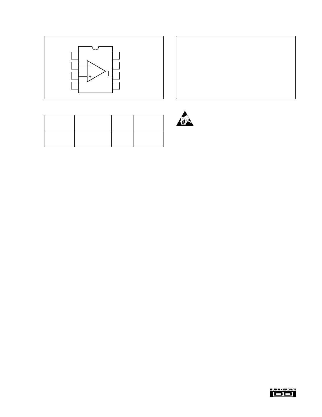
PIN CONFIGURATION
Top View DIP/SOIC
Offset Trim
–In
+In
V–
1
2
3
4
Offset Trim
8
V+
7
V
6
O
No Internal Connection
5
ABSOLUTE MAXIMUM RATINGS
Power Supply Voltage .......................................................................±22V
Differential Input Voltage ...................................................................±30V
Input Voltage ....................................................................................... ±V
Output Short Circuit .................................................................Continuous
Operating Temperature:
Plastic DIP (P), SO-8 (S) .............................................. –40°C to +85°C
θ
(PDIP) ................................................................................. 100°C/W
JA
θ
(SOIC) ................................................................................. 160°C/W
JA
Storage Temperature:
Plastic DIP (P), SO-8 (S) ............................................ –65°C to +125°C
Junction Temperature.................................................................... +150°C
Lead Temperature (soldering, 10s) P packages ........................... +300°C
(soldering, 3s) S package ............................... +260°C
S
PACKAGE/ORDERING INFORMATION
PACKAGE
DRAWING TEMPERATURE
PRODUCT PACKAGE NUMBER
OPA177FP 8-Pin Plastic DIP 006 –40°C to +85°C
OPA177GP 8-Pin Plastic DIP 006 –40°C to +85°C
OPA177GS SO-8 Surface-Mount 182 –40°C to +85°C
NOTE: (1) For detailed drawing and dimension table, please see end of data
sheet, or Appendix C of Burr-Brown IC Data Book.
(1)
RANGE
ELECTROSTATIC
DISCHARGE SENSITIVITY
Any integrated circuit can be damaged by ESD. Burr-Brown
recommends that all integrated circuits be handled with
appropriate precautions. ESD can cause damage ranging
from subtle performance degradation to complete device
failure. Precision integrated circuits may be more susceptible to damage because very small parametric changes
could cause the device not to meet published specifications.
Burr-Brown’s standard ESD test method consists of five
1000V positive and negative discharges (100pF in series
with 1.5kΩ) applied to each pin.
Failure to observe proper handling procedures could result
in small changes to the OPA177’s input bias current.
The information provided herein is believed to be reliable; however, BURR-BROWN assumes no responsibility for inaccuracies or omissions. BURR-BROWN assumes
no responsibility for the use of this information, and all use of such information shall be entirely at the user’s own risk. Prices and specifications are subject to change
without notice. No patent rights or licenses to any of the circuits described herein are implied or granted to any third party. BURR-BROWN does not authorize or warrant
any BURR-BROWN product for use in life support devices and/or systems.
3
OPA177
®
 Loading...