

Page 1
查询OPA137P供应商
®
OPA137
LOW COST
FET-INPUT OPERATIONAL AMPLIFIERS
Micro
FEATURES
● FET INPUT: IB = 5pA
● LOW OFFSET VOLTAGE: 1.5mV
● WIDE SUPPLY RANGE: ±2.25V to ±18V
● LOW QUIESCENT CURRENT: 220µA/channel
● EXCELLENT SPEED/POWER: 1MHz
● INPUT TO POSITIVE SUPPLY
●
Micro
SIZE PACKAGES: SOT-23-5, MSOP-8
● SINGLE, DUAL, AND QUAD
APPLICATIONS
● STRAIN GAGE AMPLIFIER
● PHOTODETECTOR AMPLIFIER
● PRECISION INTEGRATOR
● BATTERY-POWERED INSTRUMENTS
● TEST EQUIPMENT
● ACTIVE FILTERS
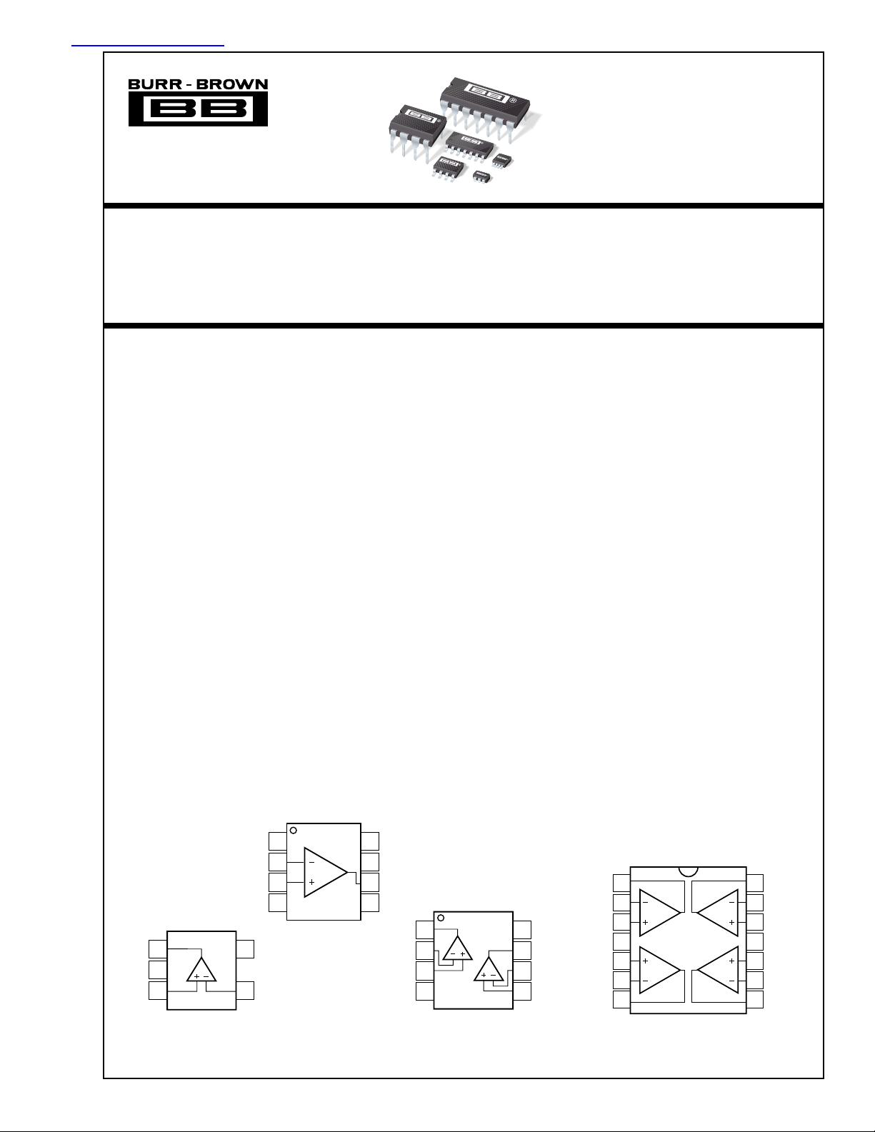
OPA137
Amplifier
OPA2137
OPA4137
OPA137
OPA2137
OPA4137
OPA4137
™
Series
DESCRIPTION
OPA137 series FET-input operational amplifiers are designed
for low cost and miniature applications. In addition to small
size (SOT-23-5 and MSOP-8 packages), they provide low
input bias current (5pA), low quiescent currrent (220µA/
channel), and high open-loop gain (94dB).
Either single (+4.5V to +36V) or dual (±2.25 to ±18V)
supplies can be used. The input common-mode voltage range
includes the positive supply—suitable for many single-supply
applications. Single, dual, and quad versions have identical
specifications for maximum design flexibility.
OPA137 op amps are easy to use and free from phase
inversion and overload problems found in some FET-input
amplifiers. High performance, including linearity, is maintained as the amplifiers swing to their specified limits. In
addition, the combination of high slew rate (3.5V/µs) and
wide bandwidth (1MHz) provide fast settling time assuring
good dynamic response. Dual and quad designs feature completely independent circuitry for lowest crosstalk and freedom
from interaction.
The single (OPA137) packages are the tiny 5-lead SOT-23-5
surface mount, SO-8 surface mount, and 8-pin DIP. The dual
(OPA2137) comes in the miniature MSOP-8 surface mount,
SO-8 surface mount, and 8-pin DIP packages. The quad
(OPA4137) packages are the SO-14 surface mount and the
14-pin DIP. All are specified from –40°C to +85°C and operate
from –55°C to +125°C. A SPICE macromodel is available for
design analysis.
NC
1
–In
2
+In
3
V–
4
OPA137
Out
1
V–
2
+In
3
SOT-23-5
International Airport Industrial Park • Mailing Address: PO Box 11400, Tucson, AZ 85734 • Street Address: 6730 S. Tucson Blvd., Tucson, AZ 85706 • Tel: (520) 746-1111 • Twx: 910-952-1111
Internet: http://www.burr-brown.com/ • FAXLine: (800) 548-6133 (US/Canada Only) • Cable: BBRCORP • Telex: 066-6491 • FAX: (520) 889-1510 • Immediate Product Info: (800) 548-6132
© 1998 Burr-Brown Corporation PDS-1438A Printed in U.S.A. August, 1998
5
4
8-Pin DIP, SO-8
V+
–In
NC
8
V+
7
Output
6
NC
5
Out A
–In A
+In A
V–
OPA2137
1
A
2
3
4
8-Pin DIP, SO-8, MSOP-8
B
V+
8
Out B
7
–In B
6
+In B
5
Out A
–In A
+In A
+In B
–In B
Out B
1
2
3
V+
4
5
6
7
OPA4137
14
AD
BC
14-Pin DIP
SO-14
13
12
11
10
9
8
Out D
–In D
+In D
V–
+In C
–In C
Out C
Page 2

SPECIFICATIONS: VS = ±15V
At TA = +25°C, RL = 10kΩ connected to ground, unless otherwise noted.
Boldface limits apply over the specified temperature range, T
PARAMETER CONDITION MIN TYP MAX MIN TYP MAX UNITS
OFFSET VOLTAGE
Input Offset Voltage V
T
= –40°C to +85°C ±2.5 ±7 ±3.5 ±15 mV
A
vs Temperature dV
vs Power Supply PSRR V
T
= –40°C to +85°C ±250 ✻ µV/V
A
Channel Separation (dual, quad) dc 0.6 ✻ µV/V
OS
/dT TA = –40°C to +85°C ±15 ✻ µV/°C
OS
INPUT BIAS CURRENT V
Input Bias Current I
vs Temperature See Typical Curve ✻
Input Offset Current I
B
OS
NOISE
Input Voltage Noise, f = 0.1 to 10Hz 2 ✻ µVp-p
Input Voltage Noise Density, f = 1kHz e
Current Noise Density, f = 1kHz i
n
n
INPUT VOLTAGE RANGE
Common-Mode Voltage Range V
Common-Mode Rejection Ratio CMRR V
CM
OPA137, OPA2137 76 84 70 ✻ dB
OPA4137 74 84 70 ✻ dB
T
= –40°C to +85°C V
A
OPA137, OPA2137 72 70 dB
OPA4137 70 70 dB
INPUT IMPEDANCE
Differential 10
Common-Mode 10
OPEN-LOOP GAIN
Open-Loop Voltage Gain A
T
= –40°C to +85°C VO = –13.8V to 13.9V 86 ✻ dB
A
OL
FREQUENCY RESPONSE
Gain-Bandwidth Product GBW 1 ✻ MHz
Slew Rate SR G = 1 3.5 ✻ V/µs
Settling Time, 0.1% G = 1, 10V Step, C
0.01% G = 1, 10V Step, C
Overload Recovery Time V
Total Harmonic Distortion + Noise THD+N G = 1, f = 1kHz, 3.5Vrms 0.05 ✻ %
OUTPUT
Voltage Output V
T
= –40°C to +85°C
A
Short-Circuit Current I
Capacitive Load Drive C
OUT
SC
LOAD
POWER SUPPLY
Specified Operating Range V
Operating Voltage Range
S
Dual Supplies ±2.25
Single Supply +4.5 +36 ✻✻V
Quiescent Current I
T
= –40°C to +85°C IO = 0 ±375 ✻ µA
A
Q
TEMPERATURE RANGE
Specified Range –40 +85 ✻✻°C
Operating Range –55 +125 ✻✻°C
Storage Range –55 +125 ✻✻°C
Thermal Resistance
SOT-23-5 Surface Mount 200 ✻ °C/W
θ
JA
MSOP-8 Surface Mount 150 ✻ °C/W
SO-8 Surface Mount 150 ✻ °C/W
8-Pin DIP 100 ✻ °C/W
SO-14 Surface Mount 100 ✻ °C/W
14-Pin DIP 80 ✻ °C/W
✻ Specifications the same as OPA137N, U, P.
NOTE: (1) At minimum power supply voltage inputs must be biased above ground in accordance with common-mode voltage range restrictions—see “Operating
Voltage” discussion.
= –40°C to +85°C.
A
OPA137N, U, P OPA137NA, UA, PA
OPA2137E, U, P OPA2137EA, UA, PA
OPA4137U, P OPA4137UA, PA
±1.5 ±3 ±2.5 ±10 mV
= ±3V to ±18V ±90 ±250 ✻✻µV/V
S
= 0V
CM
±5 ±100 ✻✻pA
±2 ±50 ✻✻pA
45 ✻ nV/√Hz
1.2 ✻ fA/√Hz
(V–) + 3 (V+) ✻✻V
= –12V to 15V
CM
= –12V to 15V
CM
10
|| 1 ✻ Ω || pF
12
|| 2 ✻ Ω || pF
VO = –13.8V to 13.9V 86 94 ✻✻ dB
= 100pF 8 ✻ µs
L
= 100pF 10 ✻ µs
L
• G = V
IN
S
(V–) + 1.2
(V–) + 1.2
1 ✻ µs
(V+) – 1.1
(V+) – 1.1
✻✻V
✻✻V
–25/+60 ✻ mA
1000 ✻ pF
±15 ✻ V
(1)
±18 ✻✻V
IO = 0 ±220 ±270 ✻✻µA
®
OPA137, 2137, 4137
2
Page 3
ABSOLUTE MAXIMUM RATINGS
Supply Voltage, V+ to V– ..................................................................... 36V
Input Voltage....................................................... (V–) –0.7V to (V+) +0.7V
Input Current ....................................................................................... 2mA
Output Short-Circuit
Operating Temperature .................................................. –55°C to +125°C
Storage Temperature...................................................... –55°C to +125°C
Junction Temperature .................................................................... +150°C
Lead Temperature (soldering, 10s) ................................................. 300°C
NOTE: (1) Stresses above these ratings may cause permanent damage.
Exposure to absolute maximum ratings for extended periods may affact device
reliability. (2) Short circuit to ground, one amplifier per package.
(2)
.............................................................. Continuous
(1)
ELECTROSTATIC
DISCHARGE SENSITIVITY
This integrated circuit can be damaged by ESD. Burr-Brown
recommends that all integrated circuits be handled with
appropriate precautions. Failure to observe proper handling
and installation procedures can cause damage.
ESD damage can range from subtle performance degradation to complete device failure. Precision integrated circuits
may be more susceptible to damage because very small
parametric changes could cause the device not to meet its
published specifications.
PACKAGE/ORDERING INFORMATION
PACKAGE SPECIFIED
DRAWING TEMPERATURE PACKAGE ORDERING TRANSPORT
PRODUCT PACKAGE NUMBER
Single
OPA137N 5-Lead SOT-23-5 Surface Mount 331 –40°C to +85°C E37
"""""OPA137N/3K Tape and Reel
OPA137NA 5-Lead SOT-23-5 Surface Mount 331 –40°C to +85°C E37
(1)
RANGE MARKING NUMBER
(3)
(3)
OPA137N/250 Tape and Reel
OPA137NA/250 Tape and Reel
"""""OPA137NA/3K Tape and Reel
OPA137U SO-8 Surface Mount 182 –40°C to +85°C OPA137U OPA137U Rails
"""""OPA137U/2K5 Tape and Reel
OPA137UA SO-8 Surface Mount 182 –40°C to +85°C OPA137UA OPA137UA Rails
"""""OPA137UA/2K5 Tape and Reel
OPA137P 8-Pin DIP 006 –40°C to +85°C OPA137P OPA137P Rails
OPA137PA 8-Pin DIP 006 –40°C to +85°C OPA137PA OPA137PA Rails
Dual
OPA2137E MSOP-8 Surface Mount 337 –40°C to +85°C E37
"""""OPA2137E/2K5 Tape and Reel
OPA2137EA MSOP-8 Surface Mount 337 –40°C to +85°C E37
(3)
(3)
OPA2137E/250 Tape and Reel
OPA2137EA/250 Tape and Reel
"""""OPA2137EA/2K5 Tape and Reel
OPA2137U SO-8 Surface Mount 182 –40°C to +85°C OPA2137U OPA2137U Rails
"""""OPA2137U/2K5 Tape and Reel
OPA2137UA SO-8 Surface Mount 182 –40°C to +85°C OPA2137UA OPA2137UA Rails
"""""OPA2137UA/2K5 Tape and Reel
OPA2137P 8-Pin DIP 006 –40°C to +85°C OPA2137P OPA2137P Rails
OPA2137PA 8-Pin DIP 006 –40°C to +85°C OPA2137PA OPA2137PA Rails
Quad
OPA4137U SO-14 Surface Mount 235 –40°C to +85°C OPA4137U OPA4137U Rails
"""""OPA4137U/2K5 Tape and Reel
OPA4137UA SO-14 Surface Mount 235 –40°C to +85°C OPA4137UA OPA4137UA Rails
"""""OPA4137UA/2K5 Tape and Reel
OPA4137P 14-Pin DIP 010 –40°C to +85°C OPA4137P OPA4137P Rails
OPA4137PA 14-Pin DIP 010 –40°C to +85°C OPA4137PA OPA4137PA Rails
NOTES: (1) For detailed drawing and dimension table, please see end of data sheet, or Appendix C of Burr-Brown IC Data Book. (2) Models with a slash (/ ) are
available only in Tape and Reel in the quantities indicated (e.g., /2K5 indicates 2500 devices per reel). Ordering 3000 pieces of “OPA137NA/3K” will get a single
3000-piece Tape and Reel. For detailed Tape and Reel mechanical information, refer to Appendix B of Burr-Brown IC Data Book. (3) Grade information is marked
on the reel.
(2)
MEDIA
The information provided herein is believed to be reliable; however, BURR-BROWN assumes no responsibility for inaccuracies or omissions. BURR-BROWN assumes no
responsibility for the use of this information, and all use of such information shall be entirely at the user’s own risk. Prices and specifications are subject to change without notice.
No patent rights or licenses to any of the circuits described herein are implied or granted to any third party. BURR-BROWN does not authorize or warrant any BURR-BROWN product
for use in life support devices and/or systems.
3
OPA137, 2137, 4137
®
Page 4

TYPICAL PERFORMANCE CURVES
At TA = +25°C, VS = ±15V, RL = 10kΩ, connected to ground, unless otherwise noted.
100
80
60
40
Gain (dB)
20
0
–20
1k
100
OPEN-LOOP GAIN/PHASE vs FREQUENCY
G
–40°C
+85°C
+25°C
1 10 100 1k 10k 100k 1M 10M
Frequency (Hz)
INPUT VOLTAGE AND CURRENT NOISE
SPECTRAL DENSITY vs FREQUENCY
Voltage Noise
POWER SUPPLY AND COMMON-MODE REJECTION
100
0
–45
φ
–90
Phase Shift (°)
–135
–180
1
10
80
60
40
PSRR, CMRR (dB)
20
0
10 100 1k 10k 100k 1M
140
120
100
CHANNEL SEPARATION vs FREQUENCY
vs FREQUENCY
+PSRR
CMRR
–PSRR
Frequency (Hz)
10
Voltage Noise (nV/√Hz)
1
0.1
10k
1k
100
10
Input Bias Current (pA)
1
0.1
–75 –50 –25 0 25 50 75 100 125
Current Noise
1 10 100 1k 10k 100k 1M
Frequency (Hz)
INPUT BIAS CURRENT vs TEMPERATURE
Temperature (°C)
1
0.1
Current Noise (fA/√Hz)
80
Dual and quad devices.
G = 1, all channels.
60
Quad measured channel
Channel Separation (dB)
A to D or B to C—other
40
combinations yield improved
rejection.
20
100 1k 10k 100k 1M
Frequency (Hz)
INPUT BIAS CURRENT
1n
100p
10p
Input Bias Current (pA)
1p
–15 –10 –5 0 5 10 15
vs INPUT COMMON-MODE VOLTAGE
Input bias current is a
function of the voltage
between the V– supply
and the inputs.
Common-Mode Voltage (V)
®
OPA137, 2137, 4137
4
Page 5

TYPICAL PERFORMANCE CURVES (CONT)
QUIESCENT CURRENT and SHORT-CIRCUIT CURRENT
vs SUPPLY VOLTAGE
Supply Voltage (V)
Quiescent Current (µA)
Short-Circuit Current (mA)
±230
±220
±210
±200
±190
±180
±170
±160
±70
±60
±50
±40
±30
±20
±10
0
0 ±5 ±10 ±15 ±20
±I
SC
I
Q
–I
SC
(IQ Per Amplifier)
AOL, CMRR, PSRR vs TEMPERATURE
Temperature (°C)
A
OL
, CMRR, PSRR (dB)
95
90
85
80
75
70
65
–75 –50 –25 0 25 50 75 100 125
PSRR
CMRR
VO = –13.8V to +13.9V
A
OL
At TA = +25°C, VS = ±15V, RL = 10kΩ, connected to ground, unless otherwise noted.
TOTAL HARMONIC DISTORTION + NOISE
vs FREQUENCY
1
G = 10
0.1
THD+N (%)
G = 1
VO = 3.5Vrms
0.01
Frequency (Hz)
QUIESCENT CURRENT and SHORT-CIRCUIT CURRENT
±400
±350
vs TEMPERATURE
(IQ Per Amplifier)
±300
+I
±250
±200
SC
I
Q
±150
Quiescent Current (µA)
±100
–I
SC
±50
0
–75 –50 –25 0 25 50 75 100 125
Temperature (°C)
100k100 1k 10k
±80
±70
±60
±50
±40
±30
±20
Short-Circuit Current (mA)
±10
0
MAXIMUM OUTPUT VOLTAGE vs FREQUENCY
30
VS = ±15V
25
CL = 200pF
VS = ±5V
CL = 100pF
Frequency (Hz)
20
15
10
Output Voltage (Vp-p)
5
0
10k 100k 1M
Maximum output voltage
without visible dynamic
distortion.
Without slew-rate
induced distortion
(V+)
(V+) –1
(V+) –2
(V+) –3
(V–) +3
(V–) +2
Output Voltage Swing (V)
(V–) +1
(V–)
0 ±2 ±4 ±6 ±8 ±10
5
OUTPUT VOLTAGE SWING vs OUTPUT CURRENT
–55°C
+125°C
+125°C
+25°C
+25°C
–55°C
Output Current (mA)
OPA137, 2137, 4137
®
Page 6

TYPICAL PERFORMANCE CURVES (CONT)
At TA = +25°C, VS = ±15V, RL = 10kΩ, connected to ground, unless otherwise noted.
OFFSET VOLTAGE PRODUCTION DISTRIBUTION
20
Typical production
18
distribution of
packaged units.
16
Single, duals, and
14
quads included.
12
10
8
6
4
Percent of Amplifiers (%)
2
0
–9–8–7–6–5–4–3–2–1
–10
100
SETTLING TIME vs CLOSED-LOOP GAIN
10V Step
012345678
Offset Voltage (mV)
0.01%
9
10
20
18
16
14
12
10
8
6
4
Percent of Amplifiers (%)
2
0
048
60
50
OFFSET VOLTAGE DRIFT
PRODUCTION DISTRIBUTION
Typical production
distribution of
packaged units.
Single, duals, and
quads included.
1216202428323640444852566064688276
Offset Voltage Drift (µV/°C)
SMALL-SIGNAL OVERSHOOT
vs LOAD CAPACITANCE
80
10
Settling Time (µs)
1
1 10 100
Closed-Loop Gain (V/V)
SMALL-SIGNAL STEP RESPONSE
20mV/div
G = 1, C
= 50pF
L
0.1%
40
30
Overshoot (%)
20
10
0
10 100 1k 10k
LARGE-SIGNAL STEP RESPONSE
5V/div
G = –1
G = +1
Load Capacitance (pF)
G = 1, C
= 50pF
L
G = +10
1µs/div
®
OPA137, 2137, 4137
5µs/div
6
Page 7

APPLICATIONS INFORMATION
OPA137 series op amps are unity-gain stable and suitable
for a wide range of general-purpose applications. Power
supply pins should be bypassed with 10nF ceramic capacitors or larger. All circuitry is completely independent in dual
and quad versions, assuring normal performance when one
amplifier in a package is overdriven or short circuited. Many
key parameters are guaranteed over the specified temperature range, –40°C to +85°C.
OPERATING VOLTAGE
OPA137 op amps can be operated on power supplies as low
as ±2.25V. Performance remains excellent with power supplies ranging from ±2.25V to ±18V (+4.5V to +36V single
supply). Most parameters vary only slightly throughout this
supply voltage range. Quiescent current and short-circuit
current vs supply voltage are shown in Typical Performance
Curves.
Operation at very low supply voltage (VS ≤ ±3V) requires
careful attention to ensure that the common-mode voltage
remains within the linear range, VCM = (V–)+3V to (V+).
Inputs may need to be biased above ground in accordance
with the common-mode voltage range restrictions for linear
operation.
HIGH-SIDE CURRENT SENSING
Many applications require the sensing of signals near the
positive supply. The common-mode input range of OPA137
op amps includes the positive rail, enabling them to be used
to sense power supply currents as shown in Figure 2.
R
1
R
2
1kΩ
20pF
R
10kΩ
0.1Ω
3
OPA137
OPA241
Load
R1 R
V
O
output
3
R
2
VO = I
Ground-referred
L
V+
Zetex
Darlington
ZTX712
INPUT VOLTAGE
The input common-mode voltage range of OPA137 series
op amps extends from (V–)+3V to the positive rail, V+. For
normal operation, inputs should be limited to this range. The
inputs may go beyond the power supplies without output
phase-reversal. Many FET-input op amps (such as TL061
types) exhibit phase-reversal of the output when the input
common-mode range is exceeded. This can occur in voltagefollower circuits, causing serious problems in control loop
applications.
Input terminals are diode-clamped to the power supply rails
for ESD protection. If the input voltage can exceed the
negative supply by 500mV, input current should be limited
to 2mA (or less). If the input current is not adequately
limited, you may see unpredicatable behavior in the other
amplifiers in the package. This is easily accomplished with
an input resistor as shown in Figure 1. Many input signals
are inherently current-limited, therefore, a limiting resistor
may not be required.
V+
I
OVERLOAD
2mA max
V
IN
Inputs are internally
clamped to V+ and V–
OPA137
V–
V
OUT
FIGURE 2. High-Side Current Monitor.
INPUT BIAS CURRENT
The input bias current is approximately 5pA at room temperature and increases with temperature as shown in the
typical performance curve “Input Bias Current vs Temperature.”
Input Bias current also varies with common-mode voltage
and power supply voltage. This variation is dependent on
the voltage between the negative power supply and the
common-mode input voltage. The effect is shown in the
typical performance curve “Input Bias Current vs CommonMode Voltage.”
R
F
1MΩ
3.3pF
I
λ
Photodiode
BPW34
C
= 75pF
D
D
OPA137
is proportional to
I
D
light intensity (radiant power)
VO = – RF I
D
FIGURE 1. Input Current Protection for Voltages Exceed-
ing the Supply Voltage.
FIGURE 3. Photodetector Amplifier.
7
OPA137, 2137, 4137
®
Page 8

SOT-23-5
(Package Drawing #331)
MSOP-8
(Package Drawing #337)
0.027
(0.686)
0.035
0.0375
(0.9525)
(0.889)
0.075
(1.905)
0.10
(2.54)
0.0375
(0.9525)
Refer to end of data sheet or Appendix C of Burr-Brown
Data Book for tolerances and detailed package drawing.
For further information on solder pads for surface-mount
devices consult Application Bulletin AB-132.
FIGURE 4. Recommended SOT-23-5 and MSOP-8 Solder Footprints.
0.016
(0.41)
0.04
(1.016)
0.19
0.0256
(0.65)
(4.83)
®
OPA137, 2137, 4137
8
Page 9

Copyright © Each Manufacturing Company.
All Datasheets cannot be modified without permission.
This datasheet has been download from :
www.AllDataSheet.com
100% Free DataSheet Search Site.
Free Download.
No Register.
Fast Search System.
www.AllDataSheet.com
 Loading...