

Page 1
查询OPA2132供应商
FET-INPUT OPERATIONAL AMPLIFIERS
O
P
A
O
P
A
1
3
2
O
1
3
2
O
P
A
2
1
3
2
High-Speed
P
A
2
1
3
O
2
P
A
4
1
3
2
O
PA4132
OPA132
OPA2132
OPA4132
SBOS054A – JANUARY 1995 – REVISED JUNE 2004
FEATURES
● FET INPUT: IB = 50pA max
● WIDE BANDWIDTH: 8MHz
● HIGH SLEW RATE: 20V/µs
● LOW NOISE: 8nV/√Hz (1kHz)
● LOW DISTORTION: 0.00008%
● HIGH OPEN-LOOP GAIN: 130dB (600Ω load)
● WIDE SUPPLY RANGE: ±2.5 to ±18V
● LOW OFFSET VOLTAGE: 500µV max
● SINGLE, DUAL, AND QUAD VERSIONS
DESCRIPTION
The OPA132 series of FET-input op amps provides highspeed and excellent dc performance. The combination of
high slew rate and wide bandwidth provide fast settling time.
Single, dual, and quad versions have identical specifications
for maximum design flexibility. High performance grades
are available in the single and dual versions. All are ideal for
general-purpose, audio, data acquisition and communications applications, especially where high source impedance
is encountered.
OPA132 op amps are easy to use and free from phase
inversion and overload problems often found in
common FET-input op amps. Input cascode circuitry provides excellent common-mode rejection and
maintains low input bias current over its wide input voltage
range. OPA132 series op amps are stable in unity gain and
provide excellent dynamic behavior over a wide range of
load conditions, including high load capacitance. Dual and
quad versions feature completely independent circuitry for
lowest crosstalk and freedom from interaction, even when
overdriven or overloaded.
Single and dual versions are available in 8-pin DIP and
SO-8 surface-mount packages. Quad is available in 14-pin
DIP and SO-14 surface-mount packages. All are specified
for –40°C to +85°C operation.
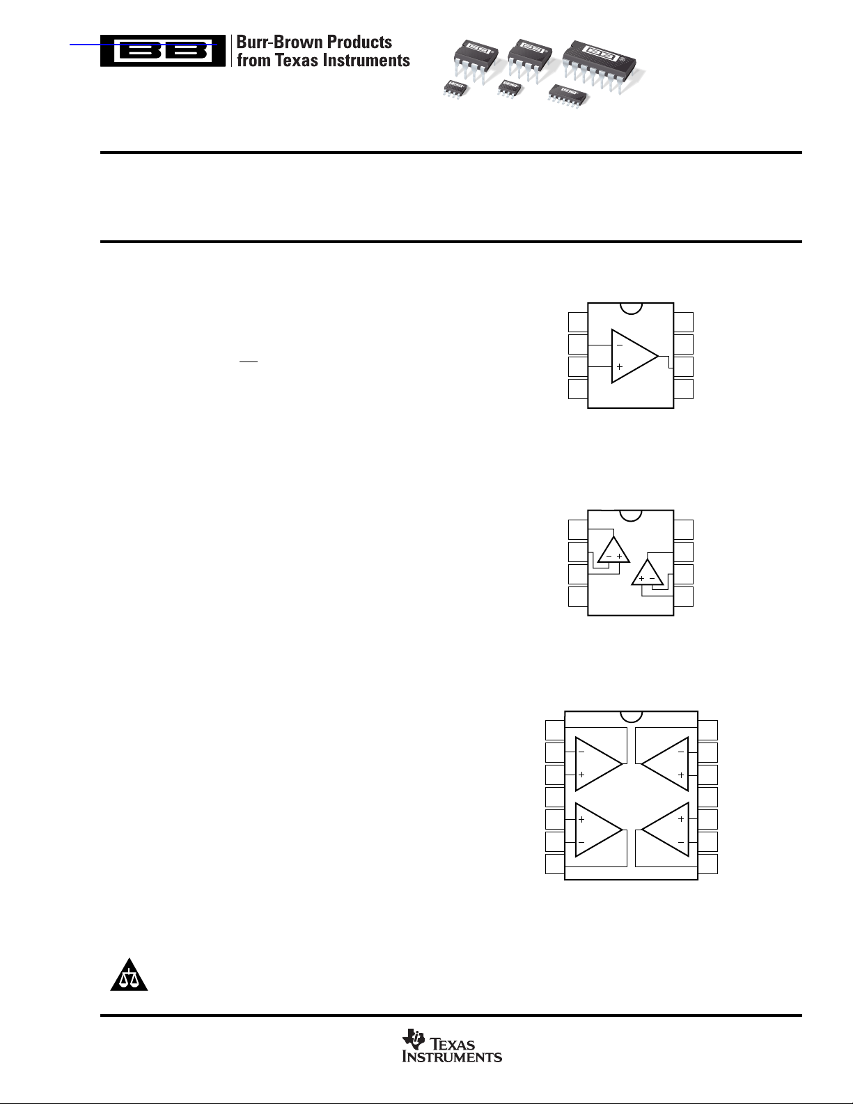
Offset Trim
–In
+In
V–
Out A
–In A
+In A
V–
Out A
–In A
+In A
V+
+In B
–In B
Out B
OPA132
1
2
3
4
8-Pin DIP, SO-8
OPA2132
1
A
2
3
4
8-Pin DIP, SO-8
1
2
3
4
5
6
7
AD
BC
14-Pin DIP
B
OPA4132
SO-14
8
7
6
5
8
7
6
5
Offset Trim
V+
Output
NC
V+
Out B
–In B
+In B
Out D
14
–In D
13
+In D
12
V–
11
+In C
10
–In C
9
Out C
8
Please be aware that an important notice concerning availability, standard warranty, and use in critical applications of
Texas Instruments semiconductor products and disclaimers thereto appears at the end of this data sheet.
All trademarks are the property of their respective owners.
PRODUCTION DATA information is current as of publication date.
Products conform to specifications per the terms of Texas Instruments
standard warranty. Production processing does not necessarily include
testing of all parameters.
Copyright © 1995-2004, Texas Instruments Incorporated
www.ti.com
Page 2

ABSOLUTE MAXIMUM RATINGS
Supply Voltage, V+ to V–.................................................................... 36V
Input Voltage ..................................................... (V–) –0.7V to (V+) +0.7V
Output Short-Circuit
Operating Temperature .................................................. –40°C to +125°C
Storage Temperature ..................................................... –55°C to +125°C
Junction Temperature...................................................................... 150 °C
Lead Temperature (soldering, 10s)................................................. 300 °C
NOTE: (1) Short-circuit to ground, one amplifier per package.
(1)
.............................................................. Continuous
PACKAGE/ORDERING INFORMATION
For the most current package and ordering information,
see the Package Option Addendum located at the end
of this data sheet.
ELECTROSTATIC
DISCHARGE SENSITIVITY
This integrated circuit can be damaged by ESD. Texas
Instruments recommends that all integrated circuits be
handled with appropriate precautions. Failure to observe proper handling and installation procedures can
cause damage.
ESD damage can range from subtle performance degradation to complete device failure. Precision integrated circuits may be more susceptible to damage
because very small parametric changes could cause
the device not to meet its published specifications.
2
www.ti.com
OPA132, 2132, 4132
SBOS054A
Page 3

SPECIFICATIONS
At TA = +25°C, VS = ±15V, unless otherwise noted.
OPA132P, U
OPA2132P, U
PARAMETER CONDITION MIN TYP MAX MIN TYP MAX UNITS
OFFSET VOLTAGE
Input Offset Voltage ±0.25 ±0.5 ±0.5 ±2mV
vs Temperature
vs Power Supply V
Channel Separation (dual and quad) R
INPUT BIAS CURRENT
Input Bias Current
vs Temperature See Typical Curve ✻
Input Offset Current
(1)
(2)
(2)
Operating Temperature Range ±2 ±10 ✻✻µV/°C
= ±2.5V to ±18V 5 15 ✻ 30 µV/V
S
= 2kΩ 0.2 ✻ µV/V
L
V
= 0V +5 ±50 ✻✻ pA
CM
V
= 0V ±2 ±50 ✻✻ pA
CM
NOISE
Input Voltage Noise
Noise Density, f = 10Hz 23 ✻ nV/√Hz
f = 100Hz 10 ✻ nV/√Hz
f = 1kHz 8 ✻ nV/√Hz
f = 10kHz 8 ✻ nV/√Hz
Current Noise Density, f = 1kHz 3 ✻ fA/√Hz
INPUT VOLTAGE RANGE
Common-Mode Voltage Range (V–)+2.5 ±13 (V+)–2.5 ✻✻✻ V
Common-Mode Rejection V
INPUT IMPEDANCE
Differential 10
Common-Mode V
= –12.5V to +12.5V 96 100 86 94 dB
CM
13
|| 2 ✻ Ω || pF
= –12.5V to +12.5V 10
CM
13
|| 6 ✻ Ω || pF
OPEN-LOOP GAIN
Open-Loop Voltage Gain R
= 10kΩ, VO = –14.5V to +13.8V 110 120 104 ✻ dB
L
R
= 2kΩ, VO = –13.8V to +13.5V 110 126 104 120 dB
L
R
= 600Ω, VO = –12.8V to +12.5V 110 130 104 120 dB
L
FREQUENCY RESPONSE
Gain-Bandwidth Product 8 ✻ MHz
Slew Rate ±20 ✻ V/µs
Settling Time: 0.1% G = –1, 10V Step, C
0.01% G = –1, 10V Step, C
Overload Recovery Time G = ±1 0.5 ✻ µs
Total Harmonic Distortion + Noise 1kHz, G = 1, V
R
R
L
= 100pF 0.7 ✻ µs
L
= 100pF 1 ✻ µs
L
= 3.5Vrms
O
= 2kΩ 0.00008 ✻ %
L
= 600Ω 0.00009 ✻ %
OUTPUT
Voltage Output, Positive R
Negative (V–)+0.5 (V–)+0.3 ✻✻ V
Positive R
Negative (V–)+1.2 (V–)+0.9 ✻✻ V
Positive R
Negative (V–)+2.2 (V–)+1.9 ✻✻ V
= 10kΩ (V+)–1.2 (V+)–0.9 ✻✻ V
L
= 2kΩ (V+)–1.5 (V+)–1.2 ✻✻ V
L
= 600Ω (V+)–2.5 (V+)–2.0 ✻✻ V
L
Short-Circuit Current ±40 ✻ mA
Capacitive Load Drive (Stable Operation) See Typical Curve ✻
POWER SUPPLY
Specified Operating Voltage ±15 ✻ V
Operating Voltage Range ±2.5 ±18 ✻✻V
Quiescent Current (per amplifier) I
= 0 ±4 ±4.8 ✻✻ mA
O
TEMPERATURE RANGE
Operating Range –40 +85 ✻✻°C
Storage –40 +125 ✻✻°C
Thermal Resistance,
8-Pin DIP 100 ✻ °C/W
θ
JA
SO-8 Surface-Mount 150 ✻ °C/W
14-Pin DIP 80 ✻ °C/W
SO-14 Surface-Mount 110 ✻ °C/W
✻ Specifications same as OPA132P, OPA132U.
NOTES: (1) Guaranteed by wafer test. (2) High-speed test at T
= 25°C.
J
OPA132PA, UA
OPA2132PA, UA
OPA4132PA, UA
OPA132, 2132, 4132
SBOS054A
www.ti.com
3
Page 4

TYPICAL PERFORMANCE CURVES
At TA = +25°C, VS = ±15V, RL = 2kΩ, unless otherwise noted.
160
140
120
100
80
60
40
Voltage Gain (dB)
20
0
–20
1k
100
OPEN-LOOP GAIN/PHASE vs FREQUENCY
G
0.1 1 10 100 1k 10k 100k 1M 10M
Frequency (Hz)
INPUT VOLTAGE AND CURRENT NOISE
SPECTRAL DENSITY vs FREQUENCY
POWER SUPPLY AND COMMON-MODE REJECTION
0
–45
φ
–90
–135
–180
Phase Shift (°)
120
100
80
60
40
PSR, CMR (dB)
20
0
10 100 1k 10k 100k 1M
160
140
CHANNEL SEPARATION vs FREQUENCY
vs FREQUENCY
–PSR
+PSR
CMR
Frequency (Hz)
RL = ∞
10
Current Noise (fA/√Hz)
Voltage Noise (nV/√Hz)
1
1
100k
10k
1k
100
10
Input Bias Current (pA)
1
0.1
–75 –50 –25 0 25 50 75 100 125
Voltage Noise
Current Noise
10 100 1k 10k 100k 1M
Frequency (Hz)
INPUT BIAS CURRENT vs TEMPERATURE
High Speed Test
Warmed Up
Quad
Dual
Single
Ambient Temperature (°C)
120
Dual and quad devices.
G = 1, all channels.
Quad measured channel
100
Channel Separation (dB)
A to D or B to C—other
combinations yield improved
rejection.
80
100 1k 10k 100k
Frequency (Hz)
INPUT BIAS CURRENT
10
9
8
7
6
5
4
3
Input Bias Current (pA)
2
1
0
–15 –10 –50 51015
vs INPUT COMMON-MODE VOLTAGE
High Speed Test
Common-Mode Voltage (V)
RL = 2kΩ
4
www.ti.com
OPA132, 2132, 4132
SBOS054A
Page 5
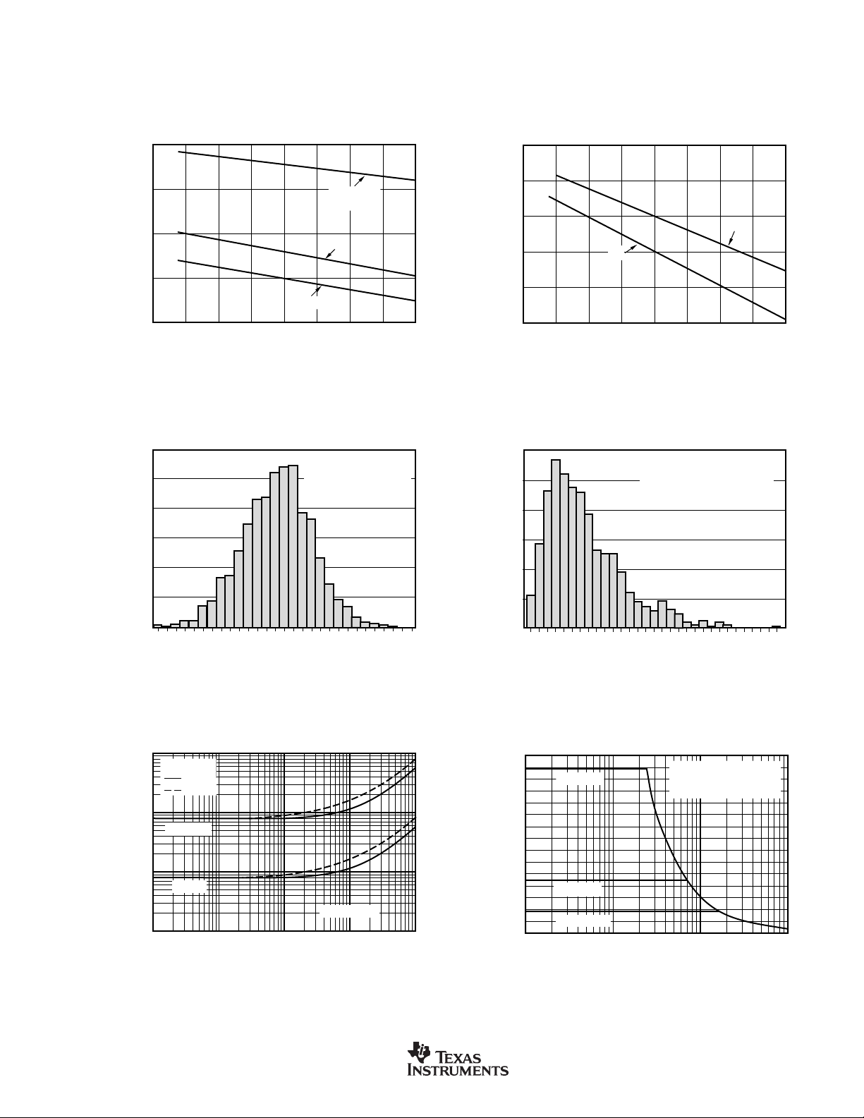
TYPICAL PERFORMANCE CURVES (Cont.)
OFFSET VOLTAGE DRIFT
PRODUCTION DISTRIBUTION
Percent of Amplifiers (%)
Offset Voltage Drift (µV/°C)
12
10
8
6
4
2
0
0.0
0.5
1.0
1.5
2.0
2.5
3.0
3.5
4.0
4.5
5.0
5.5
6.0
6.5
7.0
7.5
8.0
Typical production distribution
of packaged units. Single,
dual and quad units included.
MAXIMUM OUTPUT VOLTAGE
vs FREQUENCY
Frequency (Hz)
10k 100k 1M 10M
30
20
10
0
Output Voltage (Vp-p)
VS = ±15V
VS = ±2.5V
VS = ±5V
Maximum output voltage
without slew-rate
induced distortion
At TA = +25°C, VS = ±15V, RL = 2kΩ, unless otherwise noted.
130
120
110
, CMR, PSR (dB)
OL
A
100
90
–75 –50 –25 0 25 50 75 100 125
12
10
8
AOL, CMR, PSR vs TEMPERATURE
Open-Loop
Gain
PSR
CMR
Ambient Temperature (°C)
OFFSET VOLTAGE
PRODUCTION DISTRIBUTION
Typical production
distribution of packaged
units. Single, dual and
quad units included.
QUIESCENT CURRENT AND SHORT-CIRCUIT CURRENT
4.3
4.2
4.1
4.0
3.9
Quiescent Current Per Amp (mA)
3.8
–75 –50 –25 0 25 50 75 100 125
vs TEMPERATURE
±I
Q
Ambient Temperature (°C)
60
50
±I
SC
40
30
Short-Circuit Current (mA)
20
10
6
4
Percent of Amplifiers (%)
2
0
–800
–1400
–1200
TOTAL HARMONIC DISTORTION + NOISE
0.01
0.001
0.0001
THD+Noise (%)
0.00001
R
L
2kΩ
600Ω
G = +10
G = +1
10 100 1k 10k 100k
–600
–1000
Offset Voltage (µV)
0
–200
200
–400
vs FREQUENCY
Frequency (Hz)
400
600
800
VO = 3.5Vrms
1000
1200
1400
OPA132, 2132, 4132
SBOS054A
www.ti.com
5
Page 6

TYPICAL PERFORMANCE CURVES (Cont.)
At TA = +25°C, VS = ±15V, RL = 2kΩ, unless otherwise noted.
100
10
50mV/div
SMALL-SIGNAL STEP RESPONSE
G = 1, C
= 100pF
L
200ns/div
SETTLING TIME vs CLOSED-LOOP GAIN
0.01%
60
50
40
5V/div
LARGE-SIGNAL STEP RESPONSE
G = 1, C
1µs/div
SMALL-SIGNAL OVERSHOOT
vs LOAD CAPACITANCE
G = +1
G = –1
= 100pF
L
FPO
1
Settling Time (µs)
0.1
±1 ±10 ±100 ±1000
Closed-Loop Gain (V/V)
0.1%
OUTPUT VOLTAGE SWING vs OUTPUT CURRENT
15
14
13
12
11
10
–10
–11
–12
Output Voltage Swing (V)
–13
–14
–15
VIN = 15V
0 102030405060
VIN = –15V
125°C
85°C
125°C
Output Current (mA)
30
Overshoot (%)
20
10
0
100pF 1nF 10nF
Load Capacitance
–55°C
25°C25°C
85°C
–55°C
25°C
G = ±10
6
www.ti.com
OPA132, 2132, 4132
SBOS054A
Page 7

APPLICATIONS INFORMATION
OPA132 series op amps are unity-gain stable and suitable
for a wide range of general-purpose applications. Power
supply pins should be bypassed with 10nF ceramic capacitors or larger.
OPA132 op amps are free from unexpected output phasereversal common with FET op amps. Many FET-input op
amps exhibit phase-reversal of the output when the input
common-mode voltage range is exceeded. This can occur in
voltage-follower circuits, causing serious problems in
control loop applications. OPA132 series op amps are free
from this undesirable behavior. All circuitry is completely
independent in dual and quad versions, assuring normal
behavior when one amplifier in a package is overdriven or
short-circuited.
V+
Trim Range: ±4mV typ
10nF
100kΩ
7
1
10nF
2
OPA132
3
V–
8
6
4
OPA132 single op amp only.
Use offset adjust pins only to null
offset voltage of op amp—see text.
FIGURE 1. OPA132 Offset Voltage Trim Circuit.
OPERATING VOLTAGE
OPA132 series op amps operate with power supplies from
±2.5V to ±18V with excellent performance. Although
specifications are production tested with ±15V supplies,
most behavior remains unchanged throughout the full
operating voltage range. Parameters which vary significantly with operating voltage are shown in the typical
performance curves.
OFFSET VOLTAGE TRIM
Offset voltage of OPA132 series amplifiers is laser trimmed
and usually requires no user adjustment. The OPA132
(single op amp version) provides offset voltage trim connections on pins 1 and 8. Offset voltage can be adjusted by
connecting a potentiometer as shown in Figure 1. This
adjustment should be used only to null the offset of the op
amp, not to adjust system offset or offset produced by the
signal source. Nulling offset could degrade the offset
voltage drift behavior of the op amp. While it is not
possible to predict the exact change in drift, the effect is
usually small.
INPUT BIAS CURRENT
The FET-inputs of the OPA132 series provide very low
input bias current and cause negligible errors in most applications. For applications where low input bias current is
crucial, junction temperature rise should be minimized. The
input bias current of FET-input op amps increases with
temperature as shown in the typical performance curve
“Input Bias Current vs Temperature.”
The OPA132 series may be operated at reduced power
supply voltage to minimize power dissipation and temperature rise. Using ±3V supplies reduces power dissipation to
one-fifth that at ±15V.
The dual and quad versions have higher total power dissipation than the single, leading to higher junction temperature.
Thus, a warmed-up quad will have higher input bias current
than a warmed-up single. Furthermore, an SOIC will generally have higher junction temperature than a DIP at the same
ambient temperature because of a larger
θ
. Refer to the
JA
specifications table.
Circuit board layout can also help minimize junction tem-
perature rise. Temperature rise can be minimized by soldering the devices to the circuit board rather than using a socket.
Wide copper traces will also help dissipate the heat by acting
as an additional heat sink.
Input stage cascode circuitry assures that the input bias
current remains virtually unchanged throughout the full
input common-mode range of the OPA132 series. See the
typical performance curve “Input Bias Current vs CommonMode Voltage.”
OPA132, 2132, 4132
SBOS054A
www.ti.com
7
Page 8

PACKAGE OPTION ADDENDUM
www.ti.com
PACKAGING INFORMATION
ORDERABLE DEVICE STATUS(1) PACKAGE TYPE PACKAGE DRAWING PINS PACKAGE QTY
OPA132P OBSOLETE PDIP P 8
OPA132P1 OBSOLETE PDIP P 8
OPA132PA OBSOLETE PDIP P 8
OPA132PA2 OBSOLETE PDIP P 8
OPA132U ACTIVE SOIC D 8 100
OPA132U/2K5 ACTIVE SOIC D 8 2500
OPA132U1 OBSOLETE PDIP P 8
OPA132UA ACTIVE SOIC D 8 100
OPA132UA/2K5 ACTIVE SOIC D 8 2500
OPA132UA2 OBSOLETE PDIP P 8
OPA2132P ACTIVE PDIP P 8 50
OPA2132PA ACTIVE PDIP P 8 50
OPA2132U ACTIVE SOIC D 8 100
OPA2132U/2K5 ACTIVE SOIC D 8 2500
OPA2132UA ACTIVE SOIC D 8 100
OPA2132UA/2K5 ACTIVE SOIC D 8 2500
OPA4132PA OBSOLETE PDIP N 14
OPA4132UA ACTIVE SOIC D 14 58
OPA4132UA/2K5 ACTIVE SOIC D 14 2500
1-Jul-2004
(1) The marketing status values are defined as follows:
ACTIVE: Product device recommended for new designs.
LIFEBUY: TI has announced that the device will be discontinued, and a lifetime-buy period is in effect.
NRND: Not recommended for new designs. Device is in production to support existing customers, but TI does not recommend using this part in
a new design.
PREVIEW: Device has been announced but is not in production. Samples may or may not be available.
OBSOLETE: TI has discontinued the production of the device.
Page 9

MECHANICAL DATA
MPDI001A – JANUARY 1995 – REVISED JUNE 1999
P (R-PDIP-T8) PLASTIC DUAL-IN-LINE
0.400 (10,60)
0.355 (9,02)
8
5
0.260 (6,60)
0.240 (6,10)
1
0.021 (0,53)
0.015 (0,38)
NOTES: A. All linear dimensions are in inches (millimeters).
B. This drawing is subject to change without notice.
C. Falls within JEDEC MS-001
4
0.070 (1,78) MAX
0.020 (0,51) MIN
0.200 (5,08) MAX
0.125 (3,18) MIN
0.100 (2,54)
0.010 (0,25)
Seating Plane
M
0.325 (8,26)
0.300 (7,62)
0.015 (0,38)
Gage Plane
0.010 (0,25) NOM
0.430 (10,92)
MAX
4040082/D 05/98
For the latest package information, go to http://www.ti.com/sc/docs/package/pkg_info.htm
POST OFFICE BOX 655303 • DALLAS, TEXAS 75265
Page 10

Page 11

Page 12

Page 13

IMPORTANT NOTICE
Texas Instruments Incorporated and its subsidiaries (TI) reserve the right to make corrections, modifications,
enhancements, improvements, and other changes to its products and services at any time and to discontinue
any product or service without notice. Customers should obtain the latest relevant information before placing
orders and should verify that such information is current and complete. All products are sold subject to TI’s terms
and conditions of sale supplied at the time of order acknowledgment.
TI warrants performance of its hardware products to the specifications applicable at the time of sale in
accordance with TI’s standard warranty. Testing and other quality control techniques are used to the extent TI
deems necessary to support this warranty . Except where mandated by government requirements, testing of all
parameters of each product is not necessarily performed.
TI assumes no liability for applications assistance or customer product design. Customers are responsible for
their products and applications using TI components. To minimize the risks associated with customer products
and applications, customers should provide adequate design and operating safeguards.
TI does not warrant or represent that any license, either express or implied, is granted under any TI patent right,
copyright, mask work right, or other TI intellectual property right relating to any combination, machine, or process
in which TI products or services are used. Information published by TI regarding third-party products or services
does not constitute a license from TI to use such products or services or a warranty or endorsement thereof.
Use of such information may require a license from a third party under the patents or other intellectual property
of the third party, or a license from TI under the patents or other intellectual property of TI.
Reproduction of information in TI data books or data sheets is permissible only if reproduction is without
alteration and is accompanied by all associated warranties, conditions, limitations, and notices. Reproduction
of this information with alteration is an unfair and deceptive business practice. TI is not responsible or liable for
such altered documentation.
Resale of TI products or services with statements different from or beyond the parameters stated by TI for that
product or service voids all express and any implied warranties for the associated TI product or service and
is an unfair and deceptive business practice. TI is not responsible or liable for any such statements.
Following are URLs where you can obtain information on other Texas Instruments products and application
solutions:
Products Applications
Amplifiers amplifier.ti.com Audio www.ti.com/audio
Data Converters dataconverter.ti.com Automotive www.ti.com/automotive
DSP dsp.ti.com Broadband www.ti.com/broadband
Interface interface.ti.com Digital Control www .ti.com/digitalcontrol
Logic logic.ti.com Military www.ti.com/military
Power Mgmt power.ti.com Optical Networking www.ti.com/opticalnetwork
Microcontrollers microcontroller.ti.com Security www.ti.com/security
Telephony www.ti.com/telephony
Video & Imaging www.ti.com/video
Wireless www.ti.com/wireless
Mailing Address: Texas Instruments
Post Office Box 655303 Dallas, Texas 75265
Copyright 2004, Texas Instruments Incorporated
Page 14

Copyright © Each Manufacturing Company.
All Datasheets cannot be modified without permission.
This datasheet has been download from :
www.AllDataSheet.com
100% Free DataSheet Search Site.
Free Download.
No Register.
Fast Search System.
www.AllDataSheet.com
 Loading...