

Burr Brown OPA128SM, OPA128LM, OPA128KM, OPA128JM Datasheet
®
OPA128
Difet
®
Electrometer-Grade
OPERATIONAL AMPLIFIER
FEATURES
● ULTRA-LOW BIAS CURRENT: 75fA max
● LOW OFFSET: 500µV max
● LOW DRIFT: 5µV/
● HIGH OPEN-LOOP GAIN: 110dB min
● HIGH COMMON-MODE REJECTION:
90dB min
● IMPROVED REPLACEMENT FOR AD515
AND AD549
DESCRIPTION
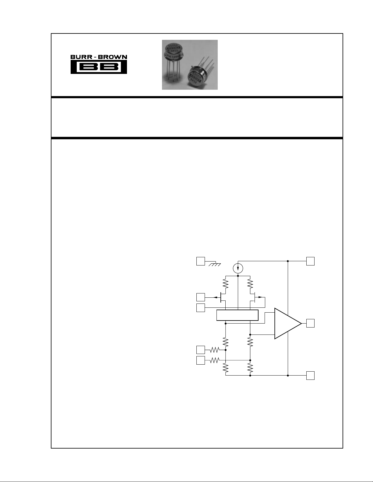
The OPA128 is an ultra-low bias current monolithic
operational amplifier. Using advanced geometry
dielectrically-isolated FET (
lithic amplifier achieves a performance level exceeding even the best hybrid electrometer amplifiers.
Laser-trimmed thin-film resistors give outstanding voltage offset and drift performance.
A noise-free cascode and low-noise processing give
the OPA128 excellent low-level signal handling capabilities. Flicker noise is very low.
The OPA128 is an improved pin-for-pin replacement
for the AD515.
®
Difet
Burr-Brown Corp.
°C max
Difet
®
) inputs, this mono-
APPLICATIONS
● ELECTROMETER
● MASS SPECTROMETER
● CHROMATOGRAPH
● ION GAUGE
● PHOTODETECTOR
● RADIATION-HARD EQUIPMENT
Case (Guard)
8
–In
2
3
+In
Trim
1
5
Trim
Noise-Free
Cascode
28kΩ
Ω1k
Ω1k
2kΩ 2kΩ
OPA128 Simplified Circuit
28kΩ
7
+V
CC
6
Output
4
–V
CC
International Airport Industrial Park • Mailing Address: PO Box 11400 • Tucson, AZ 85734 • Street Address: 6730 S. Tucson Blvd. • Tucson, AZ 85706
Tel: (520) 746-1111 • Twx: 910-952-1111 • Cable: BBRCORP • Telex: 066-6491 • FAX: (520) 889-1510 • Immediate Product Info: (800) 548-6132
©
1986 Burr-Brown Corporation PDS-653E Printed in U.S.A. May, 1995
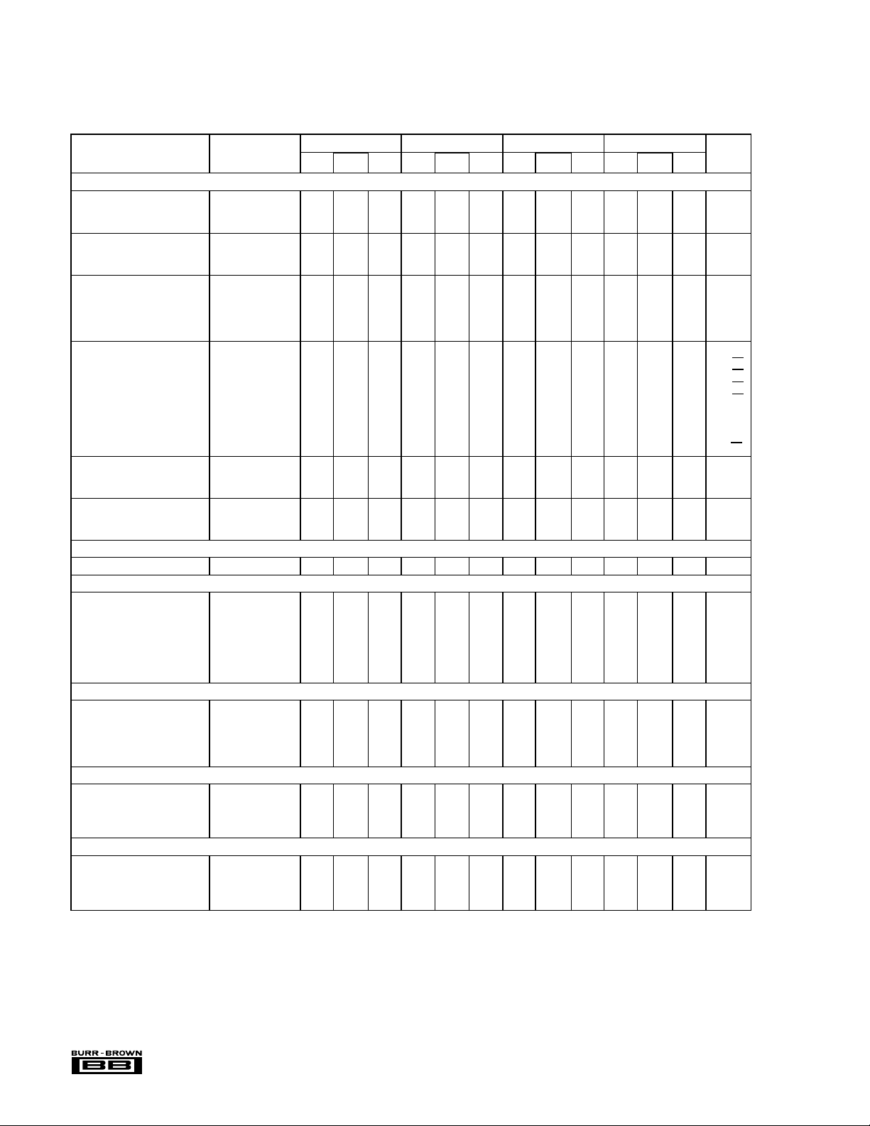
SPECIFICATIONS
ELECTRICAL
At V
= ±15VDC and TA = +25°C unless otherwise noted. Pin 8 connected to ground.
CC
OPA128JM OPA128KM OPA128LM OPA128SM
PARAMETER CONDITIONS MIN TYP MAX MIN TYP MAX MIN TYP MAX MIN TYP MAX UNITS
INPUT
BIAS CURRENT
Input Bias Current VCM = 0VDC,
OFFSET CURRENT
Input Offset Current VCM = 0VDC,
OFFSET VOLTAGE
Input Offset Voltage VCM = 0VDC ±260 ±1000 ±140 ±500 ±140 ±500 ±140 ±500 µV
Average Drift T
Supply Rejection 80 120 90 120 90 120 90 120 dB
NOISE
Voltage: f
f
f
f
f
f
Current: f
f
IMPEDANCE
Differential 10
Common-Mode 10
VOLTAGE RANGE
Common-Mode Input Range ±10 ±12 ±10 ±12 ±10 ±12 ±10 ±12 V
Common-Mode Rejection V
OPEN-LOOP GAIN, DC
Open-Loop Voltage Gain R
FREQUENCY RESPONSE
Unity Gain, Small Signal
Full Power Response 20Vp-p, R
Slew Rate V
Settling Time, 0.1% Gain = –1, R
0.01% 10V Step 10 10 10 10 µs
Overload Recovery,
50% Overdrive
RATED OUTPUT
Voltage Output R
Current Output V
Output Resistance DC, Open Loop 100 100 100 100 Ω
Load Capacitance Stability Gain = +1 1000 1000 1000 1000 pF
Short Circuit Current 10 34 55 10 34 55 10 34 55 10 34 55 mA
POWER SUPPLY
Rated Voltage ±15 ±15 ±15 ±15 VDC
Voltage Range,
Derated Performance ±5 ±18 ±5 ±18 ±5 ±18 ±5 ±18 VDC
Current, Quiescent I
TEMPERATURE RANGE
Specification Ambient Temp. 0 +70 0 +70 0 +70 –55 +125 °C
Operating Ambient Temp. –55 +125 –55 +125 –55 +125 –55 +125 °C
Storage Ambient Temp. –65 +150 –65 +150 –65 +150 –65 +150 °C
θ
Junction-Ambient 200 200 200 200 ° C/W
NOTES: (1) Offset voltage, offset current, and bias current are measured with the units fully warmed up. Bias current doubles approximately every 11°C. (2) Sample
tested. (3) Overload recovery is defined as the time required for the output to return from saturation to linear operation following the removal of a 50% input overdrive.
(4) If it is possible for the input voltage to exceed the supply voltage, a series protection resistor should be added to limit input current to 0.5mA. The input devices
can withstand overload currents of 0.3mA indefinitely without damage.
The information provided herein is believed to be reliable; however, BURR-BROWN assumes no responsibility for inaccuracies or omissions. BURR-BROWN assumes
no responsibility for the use of this information, and all use of such information shall be entirely at the user’s own risk. Prices and specifications are subject to change
without notice. No patent rights or licenses to any of the circuits described herein are implied or granted to any third party. BURR-BROWN does not authorize or warrant
any BURR-BROWN product for use in life support devices and/or systems.
(1)
R
≥ 10kΩ±150 ±300 ±75 ±150 ±40 ±75 ±75 ±150 fA
(1)
(1)
L
R
≥ 10kΩ 65 30 30 30 fA
L
= T
to T
A
MIN
MAX
±20 ±10 ±5 ±10 µV/°C
±1 ±100 ±1 ±32 ±1 ±32 ±1 ±32 µV/V
= 10Hz 92 92 92 92 nV/√Hz
O
= 100Hz 78 78 78 78 nV/√Hz
O
= 1kHz 27 27 27 27 nV/√Hz
O
= 10kHz 15 15 15 15 nV/√Hz
O
= 10Hz to 10kHz 2.4 2.4 2.4 2.4 µVrms
B
= 0.1Hz to 10Hz 4 4 4 4 µVp-p
B
= 0.1Hz to 10Hz 4.2 3 2.3 3 fA, p-p
B
= 0.1Hz to 20kHz 0.22 0.16 0.12 0.16 fA/√Hz
O
13
|| 1 1013 || 1 1013 || 1 1013 || 1 Ω || pF
15
|| 2 1015 || 2 1015 || 2 1015 || 2 Ω || pF
(4)
= ±10VDC 80 118 90 118 90 118 90 118 dB
IN
≥ 2kΩ 94 128 110 128 110 128 110 128 dB
L
(2)
= 2kΩ 47 47 47 47 kHz
L
= ±10V, RL = 2kΩ 0.53131313V/µs
O
(3)
L
Gain = –1 5 5 5 5 µs
= 2kΩ±10 ±13 ±10 ±13 ±10 ±13 ±10 ±13 V
L
= ±10VDC ±5 ±10 ±5 ±10 ±5 ±10 ±5 ±10 mA
O
= 0mADC 0.9 1.5 0.9 1.5 0.9 1.5 0.9 1.5 mA
O
0.5 1 0.5 1 0.5 1 0.5 1 MHz
= 2kΩ 5555µs
®
OPA128
2
®
ELECTRICAL (FULL TEMPERATURE RANGE SPECIFICATIONS)
At V
= ±15VDC and TA = T
CC
PARAMETER CONDITIONS MIN TYP MAX MIN TYP MAX MIN TYP MAX MIN TYP MAX UNITS
TEMPERATURE RANGE
Specification Range Ambient Temp. 0 +70 0 +70 0 +70 –55 +125 °C
INPUT
BIAS CURRENT
(1)
Input Bias Current VCM = 0VDC ±2.5 ±8 ±1.3 ±4 ±0.7 ±2 ±43 ±170 pA
OFFSET CURRENT
Input Offset Current VCM = 0VDC 1.1 0.6 0.6 18 pA
OFFSET VOLTAGE
Input Offset Voltage VCM = 0VDC ±2.2mV ±1mV ±750 ±1.5mV µV
Average Drift ±20 ±10 ±5 ±10 µV/°C
Supply Rejection 74 114 80 114 80 114 80 106 dB
VOLTAGE RANGE
Common-Mode Input Range ±10 ±11 ±10 ±11 ±10 ±11 ±10 ±11 V
Commmon-Mode Rejection V
OPEN-LOOP GAIN, DC
Open-Loop Voltage Gain R
RATED OUTPUT
Voltage Output R
Current Output V
Short Circuit Current V
POWER SUPPLY
Current, Quiescent I = 0mADC 0.9 1.8 0.9 1.8 0.9 1.8 0.9 2 mA
NOTES: (1) Offset voltage, offset current, and bias current are measured with the units fully warmed up. (2) If it is possible for the input voltage to exceed the supply
voltage, a series protection resistor should be added to limit input current to 0.5mA. The input devices can withstand overload currents of 0.3mA indefinitely without
damage.
and T
MIN
unless otherwise noted.
MAX
OPA128JM OPA128KM OPA128LM OPA128SM
(1)
(1)
±2 ±200 ±2 ±100 ±2 ±100 ±5 ±100 µV/V
(2)
= ±10VDC 74 112 80 112 80 112 74 104 dB
IN
≥ 2kΩ 90 125 104 125 104 125 90 122 dB
L
= 2k±10 ±10 ±10 ±10 V
L
= ±10VDC ±5 ±5 ±5 ±5mA
O
= 0VDC 10 22 10 22 10 22 10 18 mA
O
CONNECTION DIAGRAM
Top View
Substrate and Case
Offset
Trim
2
–In
+In
1
3
8
OPA128
4
–V
CC
7
5
+V
CC
6
Offset
Trim
Output
ABSOLUTE MAXIMUM RATINGS
Supply ...........................................................................................±18VDC
Internal Power Dissipation
Differential Input Voltage...............................................................±36VDC
Input Voltage Range ..................................................................... ±18VDC
Storage Temperature Range .......................................... –65°C to +150°C
Operating Temperature Range ....................................... –55°C to +125°C
Lead Temperature (soldering, 10s)................................................ +300°C
Output Short Circuit Duration
Junction Temperature .................................................................... +175°C
NOTES: (1) Packages must be derated based on
200°C/W. (2) Short circuit may be to power supply common only. Rating
applies to +25°C ambient. Observe dissipation limit and T
(1)
..........................................................500mW
(2)
................................................ Continuous
θ
= 150°C/W or
CA
.
J
ORDERING INFORMATION
MODEL PACKAGE RANGE max (fA)
OPA128JM TO-99 0°C to +70°C ±300
OPA128KM TO-99 0°C to +70°C ±150
OPA128LM TO-99 0°C to +70°C ±75
OPA128SM TO-99 –55°C to +125°C ±150
TEMPERATURE BIAS CURRENT,
PACKAGE INFORMATION
MODEL PACKAGE NUMBER
PACKAGE DRAWING
OPA128JM TO-99 001
OPA128KM TO-99 001
OPA128LM TO-99 001
OPA128SM TO-99 001
NOTE: (1) For detailed drawing and dimension table, please see end of data
sheet, or Appendix D of Burr-Brown IC Data Book.
θ
=
JA
(1)
3
OPA128
 Loading...